US8334862B2 - Display panel drive technique for reducing power consumption - Google Patents
Display panel drive technique for reducing power consumption Download PDFInfo
- Publication number
- US8334862B2 US8334862B2 US11/889,910 US88991007A US8334862B2 US 8334862 B2 US8334862 B2 US 8334862B2 US 88991007 A US88991007 A US 88991007A US 8334862 B2 US8334862 B2 US 8334862B2
- Authority
- US
- United States
- Prior art keywords
- pixels
- time
- data lines
- horizontal period
- switches
- Prior art date
- Legal status (The legal status is an assumption and is not a legal conclusion. Google has not performed a legal analysis and makes no representation as to the accuracy of the status listed.)
- Active, expires
Links
Images


Classifications
-
- G—PHYSICS
- G09—EDUCATION; CRYPTOGRAPHY; DISPLAY; ADVERTISING; SEALS
- G09G—ARRANGEMENTS OR CIRCUITS FOR CONTROL OF INDICATING DEVICES USING STATIC MEANS TO PRESENT VARIABLE INFORMATION
- G09G5/00—Control arrangements or circuits for visual indicators common to cathode-ray tube indicators and other visual indicators
- G09G5/003—Details of a display terminal, the details relating to the control arrangement of the display terminal and to the interfaces thereto
-
- G—PHYSICS
- G09—EDUCATION; CRYPTOGRAPHY; DISPLAY; ADVERTISING; SEALS
- G09G—ARRANGEMENTS OR CIRCUITS FOR CONTROL OF INDICATING DEVICES USING STATIC MEANS TO PRESENT VARIABLE INFORMATION
- G09G3/00—Control arrangements or circuits, of interest only in connection with visual indicators other than cathode-ray tubes
- G09G3/20—Control arrangements or circuits, of interest only in connection with visual indicators other than cathode-ray tubes for presentation of an assembly of a number of characters, e.g. a page, by composing the assembly by combination of individual elements arranged in a matrix no fixed position being assigned to or needed to be assigned to the individual characters or partial characters
- G09G3/2007—Display of intermediate tones
- G09G3/2011—Display of intermediate tones by amplitude modulation
-
- G—PHYSICS
- G09—EDUCATION; CRYPTOGRAPHY; DISPLAY; ADVERTISING; SEALS
- G09G—ARRANGEMENTS OR CIRCUITS FOR CONTROL OF INDICATING DEVICES USING STATIC MEANS TO PRESENT VARIABLE INFORMATION
- G09G3/00—Control arrangements or circuits, of interest only in connection with visual indicators other than cathode-ray tubes
- G09G3/20—Control arrangements or circuits, of interest only in connection with visual indicators other than cathode-ray tubes for presentation of an assembly of a number of characters, e.g. a page, by composing the assembly by combination of individual elements arranged in a matrix no fixed position being assigned to or needed to be assigned to the individual characters or partial characters
- G09G3/34—Control arrangements or circuits, of interest only in connection with visual indicators other than cathode-ray tubes for presentation of an assembly of a number of characters, e.g. a page, by composing the assembly by combination of individual elements arranged in a matrix no fixed position being assigned to or needed to be assigned to the individual characters or partial characters by control of light from an independent source
- G09G3/36—Control arrangements or circuits, of interest only in connection with visual indicators other than cathode-ray tubes for presentation of an assembly of a number of characters, e.g. a page, by composing the assembly by combination of individual elements arranged in a matrix no fixed position being assigned to or needed to be assigned to the individual characters or partial characters by control of light from an independent source using liquid crystals
- G09G3/3611—Control of matrices with row and column drivers
- G09G3/3648—Control of matrices with row and column drivers using an active matrix
-
- G—PHYSICS
- G09—EDUCATION; CRYPTOGRAPHY; DISPLAY; ADVERTISING; SEALS
- G09G—ARRANGEMENTS OR CIRCUITS FOR CONTROL OF INDICATING DEVICES USING STATIC MEANS TO PRESENT VARIABLE INFORMATION
- G09G3/00—Control arrangements or circuits, of interest only in connection with visual indicators other than cathode-ray tubes
- G09G3/20—Control arrangements or circuits, of interest only in connection with visual indicators other than cathode-ray tubes for presentation of an assembly of a number of characters, e.g. a page, by composing the assembly by combination of individual elements arranged in a matrix no fixed position being assigned to or needed to be assigned to the individual characters or partial characters
- G09G3/34—Control arrangements or circuits, of interest only in connection with visual indicators other than cathode-ray tubes for presentation of an assembly of a number of characters, e.g. a page, by composing the assembly by combination of individual elements arranged in a matrix no fixed position being assigned to or needed to be assigned to the individual characters or partial characters by control of light from an independent source
- G09G3/36—Control arrangements or circuits, of interest only in connection with visual indicators other than cathode-ray tubes for presentation of an assembly of a number of characters, e.g. a page, by composing the assembly by combination of individual elements arranged in a matrix no fixed position being assigned to or needed to be assigned to the individual characters or partial characters by control of light from an independent source using liquid crystals
- G09G3/3611—Control of matrices with row and column drivers
- G09G3/3685—Details of drivers for data electrodes
- G09G3/3688—Details of drivers for data electrodes suitable for active matrices only
-
- G—PHYSICS
- G09—EDUCATION; CRYPTOGRAPHY; DISPLAY; ADVERTISING; SEALS
- G09G—ARRANGEMENTS OR CIRCUITS FOR CONTROL OF INDICATING DEVICES USING STATIC MEANS TO PRESENT VARIABLE INFORMATION
- G09G2310/00—Command of the display device
- G09G2310/02—Addressing, scanning or driving the display screen or processing steps related thereto
- G09G2310/0235—Field-sequential colour display
-
- G—PHYSICS
- G09—EDUCATION; CRYPTOGRAPHY; DISPLAY; ADVERTISING; SEALS
- G09G—ARRANGEMENTS OR CIRCUITS FOR CONTROL OF INDICATING DEVICES USING STATIC MEANS TO PRESENT VARIABLE INFORMATION
- G09G2310/00—Command of the display device
- G09G2310/02—Addressing, scanning or driving the display screen or processing steps related thereto
- G09G2310/0243—Details of the generation of driving signals
- G09G2310/0248—Precharge or discharge of column electrodes before or after applying exact column voltages
Definitions
- the present invention relates to a display apparatus and, more specifically, to a technique for time-divisionally driving a plurality of data lines by a single amplifier.
- display panels are required to have an increased number of data lines (or signal lines), with reduced spacing between adjacent data lines.
- One problem caused by the increase in the number of signal lines and the decrease in the spacing therebetween is the difficulty in providing sufficient pitches for external wirings that provides electrical connections between data lines to a display panel driver.
- the decrease in the spacing between the data lines decreases the pitch allowed to the external wirings, which makes it difficult to connect the display panel with the display panel driver for driving the display panel.
- Another problem is the increase in the number of amplifiers used to drive the data lines within the display driver. The increase in the number of amplifiers undesirably makes the driver large-scaled and increases the cost of the display driver.
- Japanese Laid-Open Patent Application No. Jp-A Heisei 11-327518 discloses a liquid crystal display apparatus that is designed to drive three data lines by a single amplifier.
- FIG. 1 illustrates the structure of the liquid crystal display apparatus disclosed in this Japanese Laid-Open Patent Application.
- the liquid crystal display apparatus of FIG. 1 includes; a liquid crystal display panel 100 ; a common voltage generator circuit 104 ; a driver IC 107 ; and a switch control circuit 108 .
- the liquid crystal display panel 100 includes: gate lines (scanning lines) 101 : data lines 102 R, 102 G, and 102 B; and a common electrode 103 . Pixels are provided at respective intersections of the gate lines 101 and the data lines 102 R, 102 G, 102 B.
- the gate lines 101 are driven by a vertical drive circuit 105 .
- Switches 106 R, 106 G, and 106 B are provided for the data lines 102 R, 102 G, and 102 B, respectively, and each set of the switches 106 R, 106 G, and 106 B are commonly connected to the same output of the driver IC.
- the switches 106 R, 106 G, and 106 B are turned on and off by switch control pulses SL 1 , SL 2 , and SL 3 received from a switch control circuit 108 , respectively.
- the data lines to be driven are selected by the switches 106 R, 106 G, and 106 B.
- the driver IC 107 includes sampling circuits 111 , memories 112 , D/A converters 113 , and output amplifiers 114 .
- Pixel data of respective pixels that is, data indicative of the grayscale levels of respective pixels
- the D/A converters 113 each generate an analog grayscale voltage corresponding to the image data stored in the associated memories 112 .
- the output amplifiers 114 each drive the data line selected by the switches 106 R, 106 G, and 106 B to the same drive voltages as the analog grayscale voltages received from the D/A converters 113 .
- FIG. 2 is a timing chart illustrating the operation of the liquid crystal display apparatus of FIG. 1 , particularly the procedure of driving three target pixels positioned at the intersections of the data lines 102 Rn, 102 Gn, and 102 Bn and the gate line 101 m .
- the three target pixels are driven through the following procedure. After the voltage Vg of the gate line 101 m is pulled up to “High” level, the switch control pulses SL 1 , SL 2 , and SL 3 are successively supplied to successively turn on the switches 106 Rn, 106 Gn, and 106 Bn.
- FIG. 3 is a block diagram illustrating the structure of the liquid crystal display apparatus disclosed in this Japanese Laid-Open Patent Application.
- This liquid crystal display apparatus is configured to precharge all of the data lines to a predetermined amendment voltage Vamd before actually driving the data lines so as to suppress vertical crosstalk (display unevenness in the direction along the data lines).
- the data line precharge is also effective to reduce the power consumption of the liquid crystal display apparatus.
- the liquid crystal display apparatus of FIG. 3 includes: a display panel 201 ; a gate line drive circuit 203 ; a data line drive circuit 204 ; a control circuit 205 ; and a frame memory 206 .
- the display panel 201 includes data lines X 1 to Xm and gate lines Y 1 to Yn, and pixels 202 are provided at respective intersections of the data lines X 1 to Xm and the gate lines Y 1 to Yn.
- the gate line drive circuit 203 drives the gate lines Y 1 to Yn, while the data line drive circuit 204 drives the data lines X 1 to Xm.
- the data line drive circuit 204 includes a driver IC 241 and a time-division circuit 242 .
- the driver IC 241 includes output lines DO 1 to DOi, and every three data lines are connected to the same output line through the time-division circuit 242 .
- the time-division circuit 242 includes three switches 243 , 244 , and 245 for each of the every three data lines.
- the switches 243 , 244 , and 245 connect or disconnect the three data lines to/from the associated output pins in response to selection signals SS 1 , SS 2 , and SS 3 received from the control circuit 205 , respectively.
- FIG. 4 is a timing chart illustrating the operation of the liquid crystal display apparatus of FIG. 3 , particularly, the procedure for driving three pixels positioned at the intersections of the data lines X 1 to X 3 and the gate line Y 1 .
- the three pixels are driven through the following procedure. After activation of the gate line Y 1 , all the control signals SS 1 to SS 3 are pulled up to the “High” level to turn on the switches 243 , 244 , and 245 .
- the turn-on of the switches 243 , 244 , and 245 allows the data lines X 1 to X 3 to be electrically connected with the output pin PIN 1 of the driver IC 241 .
- the amendment voltage Vamd is then outputted from the output line DO 1 with the switches 243 , 244 , and 244 turned on, so that the data lines X 1 to X 3 are precharged to the amendment voltage Vamd.
- the control signals SS 1 to SS 3 are all pulled down to the “Low” level. This is followed by successively pull up the control signals SS 1 to SS 3 to the “High” level to successively turn on the switches 243 , 244 , and 245 .
- drive voltages are then successively supplied from the driver IC 241 to the data lines X 1 to X 3 .
- the switches 243 , 244 , and 245 are turned off. Through this procedure, the drive voltages are written to the three pixels positioned at the intersections of the data lines X 1 to X 3 and the gate line Y 1 .
- the liquid crystal display apparatuses shown in FIGS. 1 and 3 suffer from such a problem that increased electric power is consumed in the switches used for selecting the data lines (that is, the switches 106 R, 106 G, 106 B in FIG. 1 , and the switches 243 , 244 , 245 in FIG. 3 ).
- the electric power consumed in the switch is proportional to the sum of the gate capacitance and the interconnection capacitance, and is also proportional to the square of the voltage applied to the gate of the switches.
- TFTs thin film transistors
- the voltage applied to the gate is inevitably high.
- the TFTs are requested to have a high drive ability for driving the long data lines, and this requires the TFTs to have a large gate width.
- the gate capacitance thereof is inevitably large.
- the drive voltage of the pixels may reach as high as about 20V, and this requires applying high voltage of about 20V to the gates of the TFTs. Therefore, as understood from the formula (1), the power consumption of the switches used for selecting the data lines may be unacceptably increased. The increased power consumption is an issue particularly when the liquid crystal display apparatus is used within a portable electronic device.
- a method for operating a display apparatus in which one source output of a source driver is connected with first to N-th data lines through first to N-th time division switches which method includes:
- the associated one time division switch is kept turned on during a time period from a start time of the driving the first pixel to a start time of the driving the second pixel.
- a method for operating a display apparatus in which one source output of a source driver is connected with first to N-th data lines through first to N-th time division switches which method includes:
- precharging the first to N-th data lines by outputting a predetermined precharge voltage from the source output with the first to N-th time division switches turned on;
- the associated one of the first to N-th time division switches is kept turned on during a period between a first timing when the precharging is started and a second timing when the driving the specific pixel is completed.
- precharging the first to N-th data lines by outputting a predetermined precharge voltage from the source output with the first to N-th data lines electrically connected with the at least one neutralization switch and with at least one but not all of the first to N-th time division switches turned on.
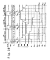
- FIG. 1 is a diagram illustrating the structure of a conventional liquid crystal display apparatus
- FIG. 2 is a timing chart illustrating the operation of the liquid crystal display apparatus of FIG. 1 ;
- FIG. 3 is a diagram illustrating the structure of another conventional liquid crystal display apparatus
- FIG. 4 is a timing chart showing the operation of the liquid crystal display apparatus of FIG. 3 ;
- FIG. 5 is a diagram illustrating an exemplary the structure of a liquid crystal display apparatus according to a first embodiment
- FIG. 6 is a block diagram of an equivalent circuit showing the structure of pixels
- FIG. 7 is a block diagram showing an exemplary structure of a source driver according to the first embodiment
- FIG. 8 is a timing chart illustrating an exemplary operation of the liquid crystal display apparatus according to the first embodiment
- FIG. 9 is a timing chart illustrating an exemplary operation of a liquid crystal display apparatus according to a comparative example
- FIG. 10 is an illustration showing an exemplary structure of the liquid crystal display apparatus according to the first embodiment, in the case that six data lines are connected to each source output;
- FIG. 11 is a timing chart illustrating an exemplary operation of the liquid crystal display apparatus of FIG. 10 ;
- FIG. 12 is a diagram illustrating an exemplary structure of a liquid crystal display apparatus according to a second embodiment
- FIG. 13 is a timing chart illustrating an exemplary operation of the liquid crystal display apparatus according to the second embodiment
- FIG. 14 is a timing chart illustrating an exemplary operation of a liquid crystal display apparatus according to a comparative example
- FIG. 15 is a timing chart illustrating an exemplary operation of the liquid crystal display apparatus of FIG. 12 when the 2H inversion drive technique is used;
- FIG. 16 is a diagram illustrating an exemplary structure of the liquid crystal display apparatus according to the second embodiment, in the case that where six data lines are connected to each source output;
- FIG. 17 is a timing chart illustrating an exemplary operation of the liquid crystal display apparatus of FIG. 16 ;
- FIG. 18 is a timing chart illustrating an exemplary operation of the liquid crystal display apparatus of FIG. 16 when the 2H inversion drive is used;
- FIG. 19 is a block diagram illustrating an exemplary structure of a source driver of a liquid crystal display apparatus according to a third embodiment
- FIG. 20 is a timing chart illustrating an operation of the liquid crystal display apparatus according to the third embodiment.
- FIG. 21 is a timing chart illustrating an operation of a liquid crystal display apparatus according to a comparative example
- FIG. 22 is a timing chart illustrating another exemplary operation of the liquid crystal display apparatus according to the third embodiment.
- FIG. 23 is a timing chart illustrating still another exemplary operation of the liquid crystal display apparatus according to the third embodiment.
- FIG. 24 is a timing chart illustrating an operation of the liquid crystal display apparatus of FIG. 20 when the 2H inversion drive is used;
- FIG. 25 is a timing chart illustrating a preferred operation of the liquid crystal display apparatus according to the third embodiment.
- FIG. 26 is a timing chart illustrating a preferred operation of the liquid crystal display apparatus of FIG. 20 when the 2H inversion drive technique is used;
- FIG. 27 is a timing chart illustrating an operation of the liquid crystal display apparatus according to the third embodiment, in the case that six data lines are connected to each source output;
- FIG. 28 is a timing chart illustrating an exemplary operation of the liquid crystal display apparatus according to the third embodiment when six data lines are connected to each source output in the case that the 2H inversion drive technique is used;
- FIG. 29 is a timing chart illustrating a preferred operation of the liquid crystal display apparatus of the third embodiment, in the case that six data lines are connected to each source output;
- FIG. 30 is a timing chart illustrating a preferred operation of the third embodiment when six data lines are connected to each source output in the case that the 2H inversion drive technique is used;
- FIG. 31 is a diagram illustrating an exemplary structure of a liquid crystal display apparatus according to a fourth embodiment
- FIG. 32 is a timing chart illustrating an exemplary operation of the liquid crystal display apparatus according to the fourth embodiment.
- FIG. 33 is a timing chart illustrating an exemplary operation of a liquid crystal display apparatus according to a comparative example
- FIG. 34 is a timing chart illustrating an operation of the liquid crystal display apparatus of FIG. 31 when the 2H inversion drive technique is used;
- FIG. 35 is a diagram illustrating another exemplary structure of the liquid crystal display apparatus according to the fourth embodiment.
- FIG. 36 is a timing chart illustrating an exemplary operation of the liquid crystal display apparatus of FIG. 35 ;
- FIG. 37 is a timing chart illustrating a preferred operation of the liquid crystal display apparatus of FIG. 31 ;
- FIG. 38 is a timing chart showing another preferred operation of the liquid crystal display apparatus of FIG. 31 ;
- FIG. 39 is a timing chart showing still another preferred operation of the liquid crystal display apparatus of FIG. 31 ;
- FIG. 40 is a timing chart showing a preferred operation of the liquid crystal display apparatus of FIG. 31 when the 2H inversion drive technique is used;
- FIG. 41 is a timing chart showing an exemplary operation of the liquid crystal display apparatus of FIG. 35 , in the case that six data lines are connected to each source output;
- FIG. 42 is a timing chart showing an exemplary operation of the liquid crystal display apparatus of FIG. 35 , in the case that six data lines are connected to each source output;
- FIG. 43 is a timing chart showing an exemplary operation of the liquid crystal display apparatus of FIG. 35 , in the case that six data lines are connected to each source output.
- FIG. 5 is a block diagram illustrating an exemplary structure of a liquid crystal display apparatus according to a first embodiment of the present invention.
- the liquid crystal display apparatus includes a liquid crystal display panel 1 , a source driver 2 , and a gate driver 3 .
- the liquid crystal display panel 1 includes: data lines RD 1 to RDm, GD 1 to GDm, BD 1 to BDm; gate lines G 1 to Gn; and pixels 11 R 1 to 11 R m , 11 G 2 to 11 G m , 11 B 1 to 11 B m .
- the pixels 11 R 1 to 11 R m are used to display red color, positioned at respective intersections of the data lines RD 1 to RDm and the gate lines G 1 to Gn.
- the pixels 11 G 1 to 11 G m are used to display green color, positioned at respective intersections of the data lines GD 1 to GDm and the gate lines G 1 to Gn.
- the pixels 11 B 1 to 11 B m are used to display blue color, positioned at respective intersections of the data lines BD 1 to BDm and the gate lines G 1 to Gn.
- the data lines RD 1 to RDm may be collectively referred to as the data lines RD if it is not necessary to distinguish one from another.
- the data lines GD 1 to GDm and the data lines BD 1 to BDm may be collectively referred to as the data lines GD and the data lines BD, respectively.
- the gate lines G 1 to Gn may be collectively referred to as the gate lines G if it is not necessary to be distinguish one from another.
- the pixels 11 R 1 to 11 R m which are used to display red color, may be collectively referred to as the pixels 11 R if it is not necessary to distinguish one from another.
- the pixels 11 G 1 to 11 G m and the pixels 11 B 1 to 11 B m may be collectively referred to as the pixels 11 G and the pixels 11 B, respectively.
- the pixels 11 R, 11 G, and 11 B may be collectively referred to as the pixels 11 if it is not necessary to distinguish one from another.
- a row of the pixels 11 connected to the same gate line GS is called a “line”, and the pixels 11 connected to the gate line Gj may be collectively referred to as the pixels 11 of the j-th line.
- the liquid crystal display panel 1 additionally includes a time-division switch circuit 12 .
- the time-division switch circuit 12 includes time-division switches 13 R 1 to 13 R m , 13 G 1 to 13 G m , 13 B 1 to 13 B m .
- TFTs integrated on the liquid crystal display panel 1 are used as the time-division switches 13 R 1 to 13 R m , 13 G 1 to 13 G m , 13 B 1 to 13 B m .
- Data lines RDi, GDi, and BDi are connected to a source output Si of the source driver 2 through the time-division switches 13 R i , 13 G i , and 13 B i , respectively.
- the time-division switches 13 R i , 13 G i , and 13 B i have a function of providing an electrical connection between the source output Si and a desired data line selected from the data lines RDi, GDi, and BDi.
- the time-division switches 13 R 1 to 13 R m may be collectively referred to as the time-division switches 13 R, if it is not necessary to distinguish one from another.
- the time-division switches 13 G 1 to 13 G m and the time-division switches 13 B 1 to 13 B m may be collectively referred to as the time-division switches 13 G and the time-division switch 13 B, respectively.
- the time-division switches 13 R, 13 G, and 13 B may be collectively referred to as the time-division switches 13 if it is not necessary to discriminate one from another.
- FIG. 6 is a diagram illustrating the structure of the pixels 11 .
- the pixels 11 each include a TFT 14 and a pixel electrode 15 .
- the source of the TFT 14 is connected to the data line RD (or GD, BD), and the gate thereof is connected to the gate line G.
- the drain of the TFT 14 is connected to the pixel electrode 15 .
- the pixel electrode 15 is opposed to the common electrode 16 , and liquid crystal material is filled between the pixel electrode 15 and the common electrode 16 .
- the grayscale level (or brightness) of each pixel 11 is controlled by the voltage between the pixel electrode 15 and the common electrode 16 .
- the source driver 2 outputs drive voltages from the source outputs S 1 to Sm so as to drive the data lines RD, GD, and BD.
- the source driver 2 includes a control circuit 21 which supplies control signals RSW, GSW, and BSW to the time-division switch circuit 12 within the liquid crystal display panel 1 .
- the time-division switches 13 R 1 to 13 R m of the time-division switch circuit 12 are turned on and off in response to the control signal RSW.
- the time-division switches 13 G 1 to 13 G m are turned on and off in response to the control signal GSW
- the time-division switches 13 B 1 to 13 B m are turned on and off in response to the control signal BSW.
- the control circuit 21 supplies a gate driver control signal G_CNT to the gate driver 3 .
- the gate driver 3 scans and drives the gate lines G 1 to Gn. The timings at which the gate lines G 1 to Gn are driven are controlled by the gate driver control signal G_CNT.
- FIG. 7 is a block diagram illustrating an exemplary structure of the source driver 2 .
- the source driver 2 includes: register circuits 22 1 to 22 m ; data latch circuits 23 1 to 23 m ; multiplexers 24 1 to 24 m ; D/A converters 25 1 to 25 m ; output amplifiers 26 1 to 26 m ; and output switches 27 1 to 27 m .
- the register circuits 22 1 to 22 m latches pixel data successively transmitted thereto.
- the pixel data are data indicating the grayscale levels of respective pixels 11 .
- pixel data for one single pixel 11 is composed of six bits.
- the pixel data of three pixels of red, green, and blue are transmitted simultaneously to the register circuit 22 i .
- the register circuit 22 i latches the pixel data transmitted thereto in response to associated latch signals SRTB 1 i .
- the data latch circuits 23 1 to 23 m latch the three pixel data from the associated register circuits 22 1 , to 22 m .
- the multiplexers 24 1 to 24 m each select one from the three pixel data latched by the associated data latch circuits 23 1 to 23 m in response to selection signals RSEL, GSEL, and BSEL, and transfer the selected pixel data to the associated D/A converters 25 1 to 25 m .
- the D/A converters 25 1 to 25 m select the grayscale voltages indicated by the pixel data transmitted thereto, and output the selected grayscale voltages to the associated output amplifiers 26 1 to 26 m .
- the output amplifiers 26 1 to 26 m function as voltage followers, and drive the source outputs S 1 to Sm to the same drive voltages as the grayscale voltages received from the associated D/A converters 25 1 to 25 m .
- Output switches 27 1 to 27 m are connected between the source outputs S 1 to Sm and the output amplifiers 26 1 to 26 m , respectively.
- the output switches 27 1 to 27 m are turned off when a control signal HIZSW is pulled up to the “High” level, and turned on when the control signal HIZSW is pulled down to the “Low” level.
- the output switches 27 1 to 27 m are turned off, the source outputs S 1 to Sm are placed into the high impedance state.
- FIG. 8 is a timing chart illustrating the operation of the liquid crystal display apparatus according to the first embodiment.
- One feature of the operation of the liquid crystal display apparatus according to the first embodiment is as follows:
- the time-division switch connected to the same data line is kept turned on until the drive of the pixel 11 connected to the same data line is completed.
- the pixels 11 of the j-th line are driven in order of the pixels 11 R, 11 G, and 11 B in the j-th horizontal period.
- the pixels 11 of the (j+1)-th line are driven in the inverse order.
- the operation of the first embodiment decreases the number of times of switching the time-division switches 13 per horizontal period, thereby reducing the power consumption effectively.
- the operation of the liquid crystal display apparatus according to the first embodiment is described in detail.
- the pixels 11 of the j-th line are driven in order of the pixels 11 R, 11 G, and 11 .
- the polarities of the drive voltages supplied to adjacent pixels of the j-th line are opposite from each other. It should be noted that the polarities of drive voltages are defined on the basis of the voltage level of the common electrode 16 .
- the drive of the pixels 11 of the j-th line in the j-th horizontal period is executed in the following manner.
- the control signal RSW is being pulled up continuously from the (j ⁇ 1)-th horizontal period. That is, the time-division switches 13 R are already turned on at the beginning of the j-th horizontal period.
- the source driver 2 outputs drive voltages associated with the pixels 11 G and 11 B from the source outputs S 1 to Sm to drive the pixels 11 G and 11 B in this order.
- the gate line Gj is pulled down.
- the control signal BSW is not pulled down, so that the time-division switches 13 B are continuously kept turned on.
- the time-division switches 13 B are continuously turned on until the next horizontal period (the (j+1)-th horizontal period).
- the pixels 11 of the (j+1)-th line are driven in order of the pixels 11 B, 11 G, and 11 R. It should be noted that, after the pixels 11 B of the j-th line are driven lastly in the j-th horizontal period, the pixels 11 B of the (j+1)-th line, which are connected with the same data lines, are driven first in the (j+1)-th horizontal period.
- the control signals GSW and RSW are activated in this order.
- the time-division switches 13 G and 13 R are turned on in this order.
- the source driver 2 outputs the drive voltages associated with the pixels 11 G and 11 R from the source outputs S 1 to Sm to drive the pixels 11 G and 11 R in this order.
- the gate line Gj+1 is pulled down.
- the control signal RSW is not pulled down, so that the time-division switches 13 R are continuously kept turned on.
- the time-division switches 13 R are continuously turned on until the next horizontal period (the (j+2)-th horizontal period).
- the pixels 11 of the (j+2)-th line are driven in the same manner as those of the j-th line. Thereafter, the pixels 11 of the (j+3)-th line are driven in the (j+3)-th horizontal period in the same manner as those of the (j+1)-th line. The pixels 11 of other lines are driven in the same manner.
- the operation of the first embodiment advantageously decreases the number of times of switching the time-division switches 13 per horizontal period, thereby effectively reducing the power consumption in the time-division switches 13 .
- the advantage of the operation according to the first embodiment shown in FIG. 8 will be understood more clearly, when compared to the operation shown in FIG. 9 .
- the control signals RSW, GSW, and BSW are successively pulled up when the pixels 11 R, 11 G, and 11 B start to be driven, and the control signals RSW, GSW, and BSW are pulled down when the pixels 11 R, 11 G, and 11 B stop being driven.
- control signals RSW, GSW, and BSW are pulled up three times in total, and pulled down three times in total, for each horizontal period.
- the control signals RSW, GSW, and BSW are pulled up only twice in total, and pulled down only twice in total, for each horizontal period.
- the decrease in the number of times of the pull-down and pull-up of the control signals RSW, GSW, and BSW is equivalent to the decreased number of times of switching the time-division switches 13 . Therefore, the operation of the first embodiment shown in FIG. 8 effectively decreases the number of times of switching the time-division switches 13 .
- the operation of the liquid crystal display apparatus according to this embodiment effectively decrease the number of times of switching of the time-division switches, and thereby reduces the power consumption, effectively.
- the liquid crystal display panel 1 is provided with 6 m data lines RD 1 to RD 2 m , GD 1 to GD 2 m , and BD 1 to BD 2 m .
- Six data lines RD 2 i - 1 , GD 2 i - 1 , BD 2 i - 1 , RD 2 i , GD 2 i , and BD 2 i are connected to a single source output Si of the source driver 2 through time-division switches 13 R 2i-1 , 13 G 2i-1 , 13 B 2i-1 , 13 R 2i , 13 G 2i , and 13 B 2i , respectively.
- the control circuit 21 of the source driver 2 supplies six control signals RSW 1 , GSW 1 , BSW 1 , RSW 2 , GSW 2 , and BSW 2 to the time-division switch circuit 12 .
- the time-division switches 13 R 2i-1 , 13 G 2i-1 , 13 B 2i-1 , 13 R 2i , 13 G 2i , and 13 B 2i are turned on and off in response to the control signals RSW 1 , GSW 1 , SSW 1 , RSW 2 , GSW 2 , and BSW 2 , respectively.
- FIG. 11 is a timing chart illustrating the operation of the liquid crystal display apparatus of FIG. 10 .
- the control signal RSW 1 is being pulled up continuously from the (j ⁇ 1)-th horizontal period.
- the time-division switches 13 R 2i-1 are already turned on at the beginning of the j-th horizontal period.
- the pixels 11 of the j-th line are driven in order of the pixels 11 R 2i-1 , 11 G 2i-1 , 11 B 2i-1 , 11 R 2i , 11 G 2i , and 11 B 2i .
- hatchings indicate the periods during which the associated pixels 11 are driven.
- the gate line Gj is pulled up in driving the pixels 11 of the j-th line, and the drive voltage associated with the pixel 11 R 2i-1 is outputted from the source output Si to drive the pixel 11 R 2i-1 .
- control signals GSW 1 , BSW 1 , RSW 2 , GSW 2 , and BSW 2 are activated in this order to turn on the time-division switches 13 G 2i-1 , 13 B 2i-1 , 13 R 2i , 13 G 2i , and 13 B 2i in this order.
- the drive voltages associated with the pixels 11 G 2i-1 , 11 B 2i-1 , 11 R 2i , 11 G 2i , and 11 B 2i are outputted from the source output Si to successively drive the pixels 11 G 2i-1 , 11 B 2i-1 , 11 R 2i , 11 G 2i , and 11 B 2i .
- the gate line Gj is pulled down.
- the control signal BSW 2 is not pulled down, so that the time-division switch 13 B 2i is continuously kept turned on.
- the time-division switch 13 B 2i is continuously turned on until the next horizontal period (the (J+1)-th horizontal period),
- the pixels 11 of the (j+1)-th line are driven in order of the pixels 11 B 2i , 11 G 2i , 11 R 2i , 11 B 2i-1 , 11 G 2i-1 , and 11 R 2i-1 . More specifically, the gate line Gj+1 is pulled up, and the drive voltage associated with the pixel 11 B 2i is outputted from the source output Si. Since the control signal BSW 2 is being pulled up continuously from the j-th horizontal period, the drive voltage is supplied immediately to the data line BD 2i , when the drive voltage associated with the pixel 11 B 2i is outputted from the source output Si. Thus, the pixel 11 B 2i , is driven to the supplied drive voltage,
- control signals GSW 2 , RSW 2 , BSW 1 , GSW 1 , and RSW 1 are pulled up in this order to turn on the time-division switches 13 G 2i , 13 R 2i , 13 B 2i-1 , 13 G 2i-1 , and 13 R 2i-1 in this order.
- the drive voltages associated with the pixels 11 G 2i , 11 R 2i , 11 B 2i-1 , 11 G 2i-1 and 11 R 2i-1 are outputted from the source output Si to successively drive the pixels 11 G 2i , 11 R 2i , 11 B 2i-1 , 11 G 2i-1 , and 11 R 2i-1 .
- the gate line Gj+1 is pulled down.
- the control signal RSW 1 is not pulled down, so that the time-division switch 13 R 2i-1 is continuously kept turned on.
- the time-division switch 13 R 2i-1 is continuously turned on until the next horizontal period (the (j+2)-th horizontal period).
- the pixels 11 of the (j+2)-th line are driven in the same manner as those of the j-th line, Thereafter, the pixels 11 of the (j+3)-th line are driven in the (j+3)-th horizontal period in the same manner as those of the (j+1)-th line.
- the pixels 11 on other lines are driven in the same manner.
- This operation effectively decreases the number of times of switching of the time-division switches 13 , effectively reducing the power consumption.
- the operation of FIG. 11 only requires pulling up the control signals RSW 1 , GSW 1 , BSW 1 , RSW 2 , GSW 2 , and BSW 2 only five times in total, and pulling down the same only five times in total, for each per horizontal period, even though there are six time-division switches 13 used for switching six data lines (RD 2i-1 , GD 2 i - 1 , BD 2 i - 1 , RD 2 i , GD 2 i , and BD 2 i )
- the order of driving the pixels 11 R 2i-1 , 11 G 2i-1 , 11 B 2i-1 , 11 R 2i , 11 G 2i , and 11 B 2i may be changed as desired. It should be noted, however, that it is necessary to satisfy such a requirement that, after a certain pixel is driven lastly in a certain horizontal period, the pixel connected to the same data line as the certain pixel driven is driven first in the next horizontal period.
- FIG. 12 is a block diagram showing an exemplary structure of a liquid crystal display apparatus according to a second embodiment of the present invention.
- the liquid crystal display apparatus according to the second embodiment is adapted to precharge the data lines RD, GD, and BD.
- the liquid crystal display panel 1 of the second embodiment additionally includes a precharge line 17 and precharge switches 18 .
- the precharge line 17 is fed with a desired precharge voltage Vpre.
- the precharge switches 18 are connected between the precharge line 17 and the data lines RD, GD, and BD.
- the precharge switches 18 are turned on and off in response to an external precharge signal PSSW supplied from the control circuit 21 of the source driver 2 .
- the precharge switches IS are turned on, the data lines RD, GD, and BD are precharged to the precharge voltage Vpre.
- FIG. 13 is a timing chart showing the operation of the liquid crystal display apparatus according to the second embodiment.
- FIG. 13 shows the operation of the case where the polarities of the drive voltages supplied to the pixels 11 are inverted every line (that is, the case where the pixels 11 are driven with the 1H inversion drive technique (or one-line inversion drive)).
- all the data lines are precharged to the precharge voltage Vpre immediately after the beginning of each horizontal line.
- precharge is executed once for every n-horizontal period(s).
- the control signal RSW is being pulled up continuously from the (j ⁇ 1)-th horizontal period. That is, the time-division switches 13 R are already turned on at the beginning of the j-th horizontal period.
- a control signal HIZSW is pulled up and the source outputs S 1 to Sm are placed into the high impedance state.
- the external precharge signal PSSW is pulled up to turn on the precharge switches, and thereby the data lines RD, GD, and BD are precharged to the precharge voltage Vpre.
- the source outputs SI to Sm are kept at the high impedance state.
- the control signal HIZSW is pulled up to turn off the output switches 27 1 to 27 m , so that the outputs of the output amplifiers 26 1 to 26 m are disconnected from the source outputs S 1 to Sm (see FIG. 7 ).
- This is important to protect the output amplifiers 26 1 to 26 m .
- the time-division switches 13 R are turned on during the precharge in the present embodiment. Therefore, the precharge voltage Vpre is undesirably applied to the outputs of the output amplifiers 26 1 to 26 m , if the source outputs S 1 to Sm are electrically connected to the output amplifiers 26 1 to 26 m .
- the output switches 27 1 to 27 m are turned off so as to prevent the precharge voltage Vpre from being applied to the outputs of the output amplifiers 26 1 to 26 m .
- the pixels 11 of the j-th line are driven successively in the same manner as the first embodiment. Specifically, after completing the precharge, the gate line Gj is pulled up. The drive voltage associated with the pixels 11 R are then outputted from the source outputs S 1 to Sm and supplied to the data lines RD. This results in that the pixels 11 R are driven to desired drive voltages. Subsequently, the control signal RSW is pulled down so that the time-division switches 13 R are turned off. After the turn-off of the time-division switches 13 R, the data lines RD (and the pixels 11 R) maintain the drive voltages.
- control signals GSW and BSW are activated in this order to turn on the time-division switches 13 G and 13 B in this order.
- the drive voltages associated with the pixels 11 G and 11 B are outputted from the source outputs S 1 to Sm. This results in that the pixels 11 G and 11 B are driven in this order.
- the gate line Gj is pulled down.
- the control signal BSW is not pulled down, so that the time-division switches 13 B are continuously kept turned on.
- the time-division switches 13 B are continuously turned on until the next horizontal period (the (j+1)-th horizontal period).
- the pixels 11 of the (j+1)-th line are driven successively after the precharge of the data lines. It should be noted that, in the (j+1)-th horizontal period, the pixels 11 of the (j+1)-th line are driven in order of the pixels 11 B, 11 G, and 11 R.
- the external precharge signal PSSW is pulled up to turn on the precharge switches 18 .
- the turn-on of the precharge switches 18 allows the data lines RD, GD, and BD to be precharged to the precharge voltage Vpre.
- the source outputs S 1 to Sm are placed into the high impedance state.
- the gate line Gj+1 is pulled up and drive voltages associated with the pixels 11 B are outputted from the source outputs S 1 to Sm. Since the control signal BSW is being pulled up continuously from the j-th horizontal period, the drive voltages are supplied immediately to the data lines BD to drive the pixels 11 B to the drive voltages, when the drive voltages are outputted from the source outputs S 1 to Sm. Then, the control signal BSW is pulled down, and the time-division switches 13 B are turned off. It should be noted that, after the pixels 11 B are driven lastly among the of the j-th lines, the pixels 11 B of the (j+1)-th line, which are connected to the same data lines, are driven first in the (j+1)-th horizontal period.
- control signals GSW and RSW are pulled up in this order to turn on the time-division switches 13 G and 13 R in this order.
- the drive voltages associated with the pixels 11 G and 11 R are successively outputted from the source outputs S 1 to Sm. As a result, the pixels 11 G and 11 R are driven in this order.
- the pixels 11 of the (j+2)-th line are driven in the same manner as those of the j-th line. Thereafter, the pixels 11 on the (j+3)-th line are driven in the (j+3)-th horizontal period in the same manner as those of the (j+1)-th line. The pixels 11 of other lines are driven in the same manner.
- the above-described operation effectively decreases the number of times of switching of the time-division switches 13 , thereby reducing the power consumption in the time-division switches 13 .
- the advantage of the operation according to the second embodiment shown in FIG. 13 would be understood more clearly, when compared to the operation shown in FIG. 14 .
- the control signals RSW, GSW, and BSW are pulled up when the pixels 11 R, 11 G, and 11 B start to be driven after the precharge, and the control signals RSW, GSW, and BSW are pulled down when the pixels 11 , 11 G, and 11 B stop being driven.
- control signals RSW, GSW, and BSW are pulled up three times in total, and pulled down three times in total, for each horizontal period.
- the control signals RSW, GSW, and BSW are pulled up only twice in total, and pulled down only twice in total, for each horizontal period. Therefore, the operation of the second embodiment shown in FIG. 13 effectively decreases the number of times of switching of the time-division switches 13 .
- the operation of the liquid crystal display apparatus according to the second embodiment decreases the number of times of switching of the time-division switches, thereby reducing the power consumption, effectively.
- FIG. 15 is an illustration showing the operation of the liquid crystal display apparatus when the pixels 11 are driven with the 2H inversion drive technique.
- the external precharge signal PSSW is pulled up at the beginning of the j-th horizontal period to precharge the data lines.
- the external precharge signal PSSW is not pulled up; the data lines are not precharged at the beginning of the following (j+1)-th horizontal period.
- the data lines are precharged at the beginning of the period.
- the polarities of the drive voltages supplied to the respective pixels 11 of the (j+2)-th line driven in the (j+2)-th horizontal period are inverted from the polarities of the drive voltages supplied to the corresponding pixels 11 of the j-th line.
- control signals RSW, GSW, and BSW are pulled up only twice in total, and pulled down only twice in total, for each horizontal period. This effectively decreases the number of times of switching of the time-division switches 13 .
- FIG. 16 is a diagram illustrating an exemplary structure of such liquid crystal display apparatus.
- the liquid crystal display apparatus shown in FIG. 16 has almost the same structure as that of the liquid crystal display apparatus shown in FIG. 10 .
- the difference in the structure is that the liquid crystal display panel 1 additionally includes a precharge line 17 fed with the precharge voltage Vpre and precharge switches 18 . When the precharge switches 18 are turned on, the data lines RD, GD, and BD are precharged to the precharge voltage Vpre.
- FIG. 17 is a timing chart illustrating an exemplary operation of the liquid crystal display apparatus of FIG. 16 .
- the operation of the liquid crystal display apparatus shown in FIG. 17 is the same as the operation shown in FIG. 11 , except that all the data lines are precharged at the beginning of each horizontal period.
- the control signal RSW 1 is being pulled up continuously from the (j ⁇ 1)-th horizontal period.
- the time-division switch 13 R 2i-1 is already turned on at the beginning of the j-th horizontal period.
- the external precharge signal PSSW is pulled up to precharge all the data lines to the precharge voltage Vpre.
- the source outputs S 1 to Sm of the source driver 2 are placed into the high impedance state.
- the gate line Gj is pulled up.
- the pixels 11 of the j-th line are driven in order of the pixels 11 R 2i-1 , 11 G 2i-1 , 11 B 2i-1 , 11 R 2i , 11 G 2i , and 11 B 2i .
- hatchings indicate periods where the associated pixels 11 are driven. It should be noted that it is unnecessary to switch the control signal RSW 1 when driving the pixel 11 R 2i-2 , because the control signal RSW 1 is being pulled up continuously from the j-th horizontal period at the beginning of the j-th horizontal period.
- the gate line Gj is pulled down.
- the control signal BSW 2 is not pulled down; the time-division switch 13 B 2i is kept turned on.
- the time-division switch 13 B 2i is continuously turned on until the next horizontal period (the (j+1)-th horizontal period).
- the pixels 11 of the (j+1)-th line are driven in order of the pixels 11 B 2i , 11 R 2i , 11 B 2i-1 , 11 G 2i-1 , and 11 R 2i-1 . It is unnecessary to switch the control signal BSW 2 when driving the pixel 11 B 2i , since the control signal BSW 2 is being pulled up continuously from the j-th horizontal period at the beginning of the (j+1)-th horizontal period.
- the pixels 11 of the (j+2)-th line are driven in the same manner as those of the j-th line. Thereafter, the pixels 11 of the (j+3)-th line are driven in the (j+3)-th horizontal period in the same manner as those of the (j+1)-th line. The pixels 11 on other lines are driven in the same manner as well.
- control signals RSW 1 , GSW 1 , BSW 1 , RSW 2 , GSW 2 , and BSW 2 are pulled up only five times in total, and pulled down only five times in total, for each horizontal period.
- FIG. 18 is an illustration showing an operation of the liquid crystal display apparatus adapted to the 2H inversion drive.
- the external precharge signal PSSW is pulled up at the beginning of the j-th horizontal period, and the data lines are precharged.
- the external precharge signal PSSW is not pulled up so that the data lines are not precharged.
- the data lines are precharged at the beginning of the period.
- the operation shown in FIG. 18 also decreases the number of times of switching of the time-division switches 13 , effectively.
- a source drive is designed to provide a function of precharging the data lines.
- the data lines are precharged by driving the source outputs to the precharge voltage Vpre with the time-division switches 13 turned on, differently from the liquid crystal display apparatuses FIG. 12 and FIG. 16 , in which the precharge line 17 and the precharge switches 18 are provided for the liquid crystal display apparatus 1 .
- the structure of the source driver according to the third embodiment is modified from those of the first embodiment and the second embodiment.
- FIG. 19 is a block diagram showing a structure of the source driver 2 according to the third embodiment.
- the source driver 2 shown in FIG. 19 has a structure similar to that of the source driver shown in FIG. 7 except for that the source driver 2 according to the third embodiment additionally includes a precharge line 28 , and precharge switches 29 1 to 29 m .
- the precharge voltage Vpre is supplied to the precharge line 28 .
- the precharge switches 29 1 to 29 m are connected between the precharge line 28 and the source outputs S 1 to Sm.
- the precharge switches 29 1 to 29 m are turned on and off in response to the internal precharge signal PSW. More specifically, the precharge switches 29 1 to 29 m are turned on, when the internal precharge signal PSW is pulled up to the “High” level.
- Such structure allows the source outputs S 1 to Sm to be driven to the precharge voltage Vpre through turning on the precharge switches 29 1 to 29 m with the output switches 27 1 to 27 m turned off.
- FIG. 20 is a timing chart illustrating an exemplary operation of the liquid crystal display apparatus according to the third embodiment.
- One feature of the operation shown in FIG. 20 is that, after the precharge of the data lines through turning on all the time-division switches 13 , ones of the time-division switches 13 associated with the data lines connected to the pixels 11 to be driven first, are continuously turned on until the actual drive of the pixels 11 driven first.
- Another feature is that the time-division switches 13 associated with the data lines connected to the pixels 11 driven lastly in each horizontal period are continuously turned on until the following precharge of the data lines.
- control signal BSW is being activated continuously from the (j ⁇ 1)-th horizontal period.
- the time-division switches 13 B are already turned on at the beginning of the j-th horizontal period.
- the control signal HIZSW is pulled up to place the source outputs S 1 to Sm into the high impedance state.
- the internal precharge signal PSW is pulled up to drive the source outputs S 1 to Sm to the precharge voltage Vpre.
- the control signals RSW and GSW are also pulled up simultaneously with the pull-up of the internal precharge signal PSW.
- all the time-division switches 13 are turned on. Accordingly, the respective data lines are electrically connected to the corresponding source outputs S 1 to Sm, so that all the data lines are driven to the precharge voltage Vpre.
- the internal precharge signal PSW is pulled down, and the source outputs S 1 to Sm are returned to the high impedance state.
- the control signals GSW and BSW are pulled down to turn off the time-division switches 13 G and 13 B.
- control signal RSW is not pulled down after the precharge of the data lines is completed.
- the time-division switches 13 R are continuously turned on. As will be described later, this aims to decrease the number of times of switching of the time-division switches 13 .
- the pixels 11 of the j-th line are driven in order of the pixels 11 R, 11 G, and 11 B. Specifically, after completing the precharge, the gate line Gj is pulled up. Further, the drive voltages associated with the pixels 11 R are outputted from the source outputs S 1 to Sm, and supplied to the data lines RD. This allows the pixels 11 R to be driven to desired drive voltages. The control signal RSW is then pulled down so that the time-division switches 13 R are turned off. The data lines RD (and the pixels 11 R) are kept at the drive voltages.
- control signals GSW and BSW are successively pulled up in this order, so that the time-division switches 13 G and 13 B are turned on in this order.
- the drive voltages associated with the pixels 11 G and pixels 11 B are outputted from the source outputs Si to drive the pixels 11 G and 11 B in this order.
- the gate line Gj is pulled down.
- the control signal BSW is not pulled down, so that the time-division switches 13 B are kept turned on.
- the time-division switches 13 B are continuously turned on until the next horizontal period (the (j+1)-th horizontal period).
- the pixels 11 of the (j+1)-th line are also driven in the same manner.
- the pixels 11 on other lines are driven in the same manner as well.
- Such operation effectively decreases the number of times of switching the time-division switches 13 , thereby effectively reducing the power consumption in the time-division switches 13 .
- the advantage of the operation according to the third embodiment shown in FIG. 20 would be understood more clearly when compared to the operation shown in FIG. 21 .
- all the control signals RSW, GSW, and BSW are pulled down when the precharge is completed, and the control signals RSW, GSW, and BSW are pulled up successively thereafter. With this, the pixels 11 R, 11 G, and 11 B are driven successively.
- control signals RSW, GSW, and BSW are pulled up six times in total, and pulled down six times in total, for each horizontal period.
- the control signals RSW, GSW, and BSW are pulled up only four times in total, and pulled down only four times in total, for each horizontal period.
- the reduction of the number of times of the pull-down and pull-up of the control signals RSW, GSW, and BSW is equivalent to the reduction of the number of times of switching of the time-division switches 13 .
- the operation of the third embodiment shown in FIG. 20 effectively decreases the number of times of switching of the time-division switches 13 .
- control signal BSW may be pulled down after the drive of the pixels 11 B is completed, as shown in FIG. 22 .
- the control signal RSW is continuously pulled up after the precharge also in this case.
- the control signals RSW, GSW, and BSW are pulled up five times in total, and pulled down five times in total, for each horizontal period.
- the operation of FIG. 22 effectively reduces the number of times of switching of the time-division switches 13 compared to the typical operation shown in FIG. 21 , although it is larger than that of the operation shown in FIG. 20 .
- control signal RSW may be pulled down after the precharge is completed, as shown in FIG. 23 .
- the control signal BSW is not pulled down until the beginning of the next horizontal period (the (j+1)-th horizontal period) after the drive of the pixels 11 B is completed, so that the time-division switches 13 B are kept turned on.
- the operation of FIG. 23 effectively reduces the number of times of switching of the time-division switches 13 compared to the typical operation shown in FIG. 21 , even though it is larger than that of the operation shown in FIG. 20 .
- the 2H inversion technique may be used in the third embodiment, which involves inverting the polarities of the drive voltages the pixels every two lines.
- the data lines are precharged in every other horizontal period.
- FIG. 24 is a diagram illustrating the operation of the liquid crystal display apparatus according to the third embodiment when the 2H inversion drive is used.
- the control signal BSW is continuously activated from the (j ⁇ 1)-th horizontal period. That is, the time-division switches 13 B are already turned on at the beginning of the j-th horizontal period.
- the control signal HIZSW is pulled up to place the source outputs S 1 to Sm into the high impedance state.
- the internal precharge signal PSW is pulled up to turn on the precharge switches 29 1 to 29 m . This achieves driving the source outputs S 1 to Sm to the precharge voltage Vpre.
- the control signals RSW, GSW, and BSW are also pulled up. As a result, all the time-division switches 13 are turned on. Accordingly, the data lines are connected to the associated source outputs S 1 to Sm, so that all the data lines are driven to the precharge voltage Vpre.
- the internal precharge signal PSW is pulled down, and the source outputs S 1 to Sm are returned to the high impedance state.
- the control signals GSW and BSW are pulled down, so that the time-division switches 13 G and 13 B are turned off.
- the control signal RSW is not pulled down; the time-division switches 13 R are kept turned on. As will be described later, this aims to decrease the number of times of switching of the time-division switches 13 .
- the pixels 11 of the j-th line are driven in order of the pixels 11 R, 11 G, and 11 B. Specifically, after completing the precharge, the gate line Gj is pulled up. Further, the drive voltages associated with the pixels 11 R are outputted from the source outputs S 1 to Sm, and supplied to the data line RD. This allows the pixels 11 R to be driven to desired drive voltages. Subsequently, the control signal RSW is pulled down so that the time-division switches 13 R are turned off. The data lines RD (and the pixels 11 R) are kept at the drive voltages.
- control signals GSW and BSW are pulled up in this order, so that the time-division switches 13 G and 13 B are turned on in this order.
- the drive voltages associated with the pixels 11 G and 11 B are outputted from the source outputs S. This allows the pixels 11 G and 11 B to be driven in this order.
- control signal BSW is pulled down, and the gate line Gj is pulled down thereafter. It is noted that the operation of FIG. 24 is different from the operation of FIG. 20 in that the control signal BSW is pulled down after completing the drive of the pixels 11 B.
- the data lines are not precharged.
- the control signals RSW, GSW, and BSW are pulled up successively.
- the drive voltages associated with the pixels 11 R, 11 G, and 11 B are outputted from the source outputs S 1 to Sm. This allows the pixels 11 R, 11 G, and 11 B to be driven in this order.
- the gate line Gj+1 is pulled down.
- the control signal BSW is not pulled down, so that the time-division switches 13 B are kept turned on.
- the time-division switches 13 B are continuously turned on until the next horizontal period (the (j+2)-th horizontal period).
- the pixels 11 of the (j+2)-th line are driven in the same manner as those of the j-th line. Thereafter, the pixels 11 of the (j+3)-th line are driven in the (j+3)-th horizontal period in the same manner as those of the (j+1)-th line. The pixels 11 on other lines are driven in the same manner as well.
- control signals RSW, GSW, and BSW are pulled up three and a half times in total, and pulled down only three and a half times in total, for each horizontal period.
- the operation of FIG. 24 effectively decreases the number of times of switching of the time-division switches 13 .
- the pixels 11 of the j-th line may be driven in order of the pixels 11 R, 11 G, and 11 B, while the pixels 11 of the (j+1)-th line driven in the reversed order. It should be noted that, after the pixels 11 B are driven lastly among the pixels 11 of j-th line in the j-th horizontal period, the pixels 11 B, which is connected to the same data lines, are driven first in the (j+1)-th horizontal period in the operation shown in FIG. 25 .
- the control signal RSW is being activated continuously from the (j ⁇ 1)-th horizontal period in the operation of FIG. 25 .
- the time-division switches 13 R are already turned on at the beginning of the j-th horizontal period.
- the control signal HIZSW is pulled up to place the source outputs S 1 to Sm into the high impedance state.
- the internal precharge signal PSW is pulled up to turn on the precharge switches 29 1 to 29 m .
- the source outputs S 1 to Sm are driven to the precharge voltage Vpre.
- the control signals RSW and GSW are also pulled up.
- all the time-division switches 13 are turned on to provide electrical connections between the data lines and the associated source outputs S 1 to Sm, so that all the data lines are driven to the precharge voltage Vpre.
- the internal precharge signal PSW is pulled down, and the source outputs S 1 to Sm are returned to the high impedance state.
- the control signals GSW and BSW are pulled down, so that the time-division switches 13 G and 13 B are turned off.
- the control signal RSW is not pulled down; the time-division switches 13 R are continuously turned on. As will be described later, this aims to decrease the number of times of switching of the time-division switches 13 .
- the pixels 11 of the j-th line are driven in order of the pixels 11 R, 11 G, and 11 B. Specifically, after completing the precharge, the gate line Gj is pulled up. Further, the drive voltages associated with the pixels 11 R are outputted from the source outputs S 1 to Sm, and supplied to the data lines RD. As a result, the pixels 11 R are driven to desired drive voltages. Subsequently, the control signal RSW is pulled down so that the time-division switches 13 R are turned off. The data lines RD (and the pixels 11 R) are kept at the drive voltages.
- control signals GSW and BSW are pulled up in this order, so that the time-division switches 13 G and 13 B are turned on in this order.
- the drive voltages associated with the pixels 11 G and 11 B are outputted from the source outputs S.
- the pixels 11 G and 11 B are driven in this order.
- the gate line Gj is pulled down.
- the control signal BSW is not pulled down, so that the time-division switches 13 B are kept turned on.
- the time-division switches 13 B are continuously turned on until the next horizontal period (the (j+1)-th horizontal period).
- the pixels 11 of the (j+1)-th line are also driven successively after the precharge of the data lines. It should be noted that the pixels 11 of the (j+1)-th line are driven in order of the pixels 11 B, 11 G, and 11 R in the (j+1)-th horizontal period.
- the control signal HIZSW is pulled up to place the source outputs Si to Sm into the high impedance state.
- the internal precharge signal PSW is pulled up to turn on the precharge switches 29 1 - 29 m .
- the source outputs S 1 to Sm are driven to the precharge voltage Vpre.
- the control signals RSW and GSW are also pulled up.
- all the time-division switches 13 are turned on to provide electrical connections between the data lines and the associated source outputs S 1 to Sm, so that all the data lines are driven to the precharge voltage Vpre.
- the internal precharge signal PSW is pulled down, and the source outputs S 1 to Sm are returned to the high impedance state.
- the control signal BSW is not pulled down even after completing the precharge of the data lines; the time-division switches 13 B are continuously turned on. This aims to decrease the number of times of switching of the time-division switches 13 .
- the gate line Gj+1 is pulled up, and the drive voltages associated with the pixels 11 B are outputted from the source outputs S 1 to Sm. Since the control signal BSW is being pulled up continuously, the drive voltages are supplied immediately to the data lines BD to drive the pixels 11 B, when the drive voltages associated with the pixels 11 B are outputted. Subsequently, the control signal BSW is pulled down so that the time-division switches 13 B are turned off.
- control signals GSW and RSW are pulled up in this order to turn on the time-division switches 13 G and 13 R in this order.
- the drive voltages associated with the pixels 11 G and 11 R are outputted from the source outputs S 1 to Sm to drive the pixels 11 G and 11 R in this order.
- the gate line Gj+1 is pulled down.
- the control signal RSW is not pulled down, so that the time-division switches 13 R are kept turned on.
- the time-division switches 13 R are continuously turned on until the next horizontal period (the (j+2)-th horizontal period).
- the pixels 11 of the (j+2)-th line are driven in the same manner as those of the j-th line. Thereafter, the pixels 11 of the (j+3)-th line are driven in the (j+3)-th horizontal period in the same manner as those of the (j+1)-th line. The pixels 11 on other lines are driven in the same manner.
- control signals RSW, GSW, and BSW are pulled up only four times in total, and pulled down only four times in total, for each horizontal period.
- the operation of FIG. 25 effectively decreases the number of times of switching of the time-division switches 13 .
- the 2H inversion drive technique may be also used for the case when the pixels 11 of the j-th line are driven in order of the pixels 11 R, 11 G, 11 B and the pixels 11 on the (j+1)-th line are driven in the reversed order.
- the data lines are precharged in every other horizontal period.
- FIG. 26 is a diagram illustrating the operation of the liquid crystal display apparatus according to the third embodiment when the 2H inversion drive technique is used.
- the control signal RSW is continuously activated from the (j ⁇ 1)-th horizontal period.
- the time-division switches 13 R are already turned on at the start of the j-th horizontal period.
- the control signal HIZSW is pulled up to place the source outputs S 1 to Sm into the high impedance state.
- the internal precharge signal PSW is pulled up to turn on the precharge switches 29 1 - 29 m , and the source outputs S 1 -Sm are driven to the precharge voltage Vpre.
- the control signals GSW and BSW are also pulled up. As a result, all the time-division switches 13 are turned on. Accordingly, the data lines are connected to the associated source outputs S 1 -Sm, so that all the data lines are driven to the precharge voltage Vpre.
- the internal precharge signal PSW is pulled down, and the source outputs S 1 to Sm are returned to the high impedance state.
- the control signals GSW and BSW are pulled down, so that the time-division switches 13 G and 13 B are turned off.
- the control signal RSW is not pulled down.
- the time-division switches 13 R are continuously turned on. This aims to decrease the number of times of switching of the time-division switches 13 .
- the pixels 11 of the j-th line are driven in order of the pixels 11 R, 11 G, and 11 B. Specifically, after the completion of the precharge, the gate line Gj is pulled up and the drive voltages associated with the pixels 11 R are outputted from the source outputs S 1 to Sm and supplied to the data lines RD. As a result, the pixels 11 R are driven to desired drive voltages. Subsequently, the control signal RSW is pulled down so that the time-division switches 13 R are turned off. The data lines RD (and the pixels 11 R) are kept at the drive voltages.
- control signals GSW and BSW are pulled up in this order, so that the time-division switches 13 G and 13 B are turned on in this order.
- the drive voltages associated with the pixels 11 G and 11 B are outputted from the source outputs S to drive the pixels 11 G and 11 B in this order.
- the gate line Gj is pulled down.
- the control signal BSW is not pulled down, so that the time-division switches 13 B are kept turned on.
- the time-division switches 13 B are continuously turned on until the next horizontal period (the (j+1)-th horizontal period).
- the data lines are not precharged.
- the pixels 11 of the (j+1)-th line are driven in order of the pixels 11 B, 11 G, and 11 R. It should be noted that, when the pixels 11 B are driven lastly among the pixels 11 of the j-th line in the j-th horizontal period, the pixels 11 B of the (j+1)-th line, which are connected with the same data lines, are driven first in the (j+1)-th horizontal period.
- the drive voltages associated with the pixels 11 B are outputted from the source outputs S 1 to Sm. Since the control signal BSW is being pulled up continuously from the j-th horizontal period, the drive voltages are supplied immediately to the data line BD, and the pixels 11 B are driven to desired drive voltages, when the drive voltages associated with the pixels 11 B are outputted. Subsequently, the control signal BSW is pulled down so that the time-division switches 13 B are turned off.
- control signals GSW and RSW are activated in this order to turn on the time-division switches 13 G and 13 R in this order.
- the drive voltages associated with the pixels 11 G and 11 R are outputted from the source outputs S 1 to Sm to drive the pixels 11 G and 11 R in this order.
- the gate line Gj+1 is pulled down.
- the control signal PSW is not pulled down, so that the time-division switches 13 R are kept turned on.
- the time-division switches 13 R are continuously turned on until the next horizontal period (the (j+2)-th horizontal period).
- the pixels 11 of the (j+2)-th line are driven in the same manner as those of the j-th line. Thereafter, the pixels 11 of the (j+3)-th line are driven in the (j+3)-th horizontal period in the same manner as those of the (j+1)-th line. The pixels 11 on other lines are driven in the same manner.
- control signals RSW, GSW, and BSW are pulled up only three times in total, and pulled down only three times in total, for each horizontal period.
- the operation of FIG. 26 effectively decreases the number of times of switching of the time-division switches 13 .
- the operation of the liquid crystal display apparatus according to the third embodiment may be applied to a case where the number of data lines connected with each source output is other than three.
- the operation of the liquid crystal display apparatus according to the third embodiment may be applied to the case where six data lines are connected to each source output (as is the case of the structure shown in FIG. 10 ).
- the source driver 2 is requested to be adapted to output the precharge voltage Vpre from the source output, in this case.
- FIG. 27 is a timing chart illustrating an exemplary operation of the liquid crystal display apparatus according to the third embodiment, in the case that six data lines are connected to each source output.
- the operation of FIG. 27 is almost identical to the operation of FIG. 20 , except for that the operation of FIG. 27 is modified in accordance with the change in the number of data lines connected with each single source output.
- the control signal BSW 2 is being pulled up continuously from the (j ⁇ 1)-th horizontal period. Therefore, the time-division switch 13 R 2i is already turned on at the beginning of the j-th horizontal period.
- the external precharge signal PSW and the control signals RSW 1 , GSW 1 , BSW 1 , RSW 2 , GSW 2 are pulled up, and the precharge voltage Vpre is outputted from the source outputs S 1 to Sm. As a result, all the data lines are precharged to the precharge voltage Vpre.
- control signals GSW 1 , BSW 1 , RSW 2 , GSW 2 , and BSW 2 are pulled down.
- the control signal RSW 1 is continuously pulled up; in other words, the time-division switch 13 R 2i-1 is continuously turned on even after the precharge is completed.
- the gate line Gj is activated and the pixels 11 on the j-th line are driven in order of the pixels 11 R 2i-1 , 11 G 2i-1 , 11 B 2i-1 , 11 R 2i , 11 G 2i , and 11 B 2i .
- hatchings indicate the period during which the associated pixels 11 are driven. It is unnecessary to switch the control signal RSW 1 when the pixel 11 R 2i-1 is driven, since the control signal RSW 1 is continuously pulled up after the completion of the precharge.
- the gate line Gj is pulled down.
- the control signal BSW 2 is not pulled down, so that the time-division switch 13 B 2i is continuously kept turned on.
- the time-division switch 13 B 2i is continuously turned on until the next horizontal period (the (j+1)-th horizontal period).
- the pixels 11 of the (j+1)-th line are driven in the same manner as those of the j-th line.
- the pixels 11 on other lines are driven in the same manner as well.
- control signals RSW, GSW, and BSW are pulled up only ten times in total, and pulled down only ten times in total, for each horizontal period.
- the operation of FIG. 27 effectively decreases the number of times of switching of the time-division switches 13 .
- FIG. 28 is a timing chart illustrating the operation modified from the operation shown in FIG. 27 so as to be adapted to the 2H inversion drive technique.
- the internal precharge signal PSW and control signals RSW 1 , GSW 1 , BSW 1 , RSW 2 , GSW 2 , and BSW 2 are pulled up at the beginning of the j-th horizontal period, and the data lines are precharged.
- the internal precharge signal PSW is not pulled up so that the data lines are not precharged.
- the data lines are precharged.
- the polarities of the drive voltages supplied to the respective pixels 11 of the (j+2)-th line driven in the (j+2)-th horizontal period are inverted from the polarities of the drive voltages supplied to the corresponding pixels 11 of the j-th line.
- control signals RSW 1 , GSW 1 , BSW 1 , RSW 2 , GSW 2 , and BSW 2 are pulled up only eight times in total, and pulled down only eight times in total, for each horizontal period. This effectively decreases the number of times of switching of the time-division switches 13 .
- FIG. 29 is a timing chart illustrating another exemplary operation of the liquid crystal display apparatus according to the third embodiment, in the case that six data lines are connected to each source output.
- the pixels 11 of the j-th line are driven in order of the pixels 11 R 2i-1 , 11 G 2i-1 , 11 B 2i-1 , 11 R 2i , 11 G 2i , and 11 B 2i , while the pixels 11 of the (j+1)-th line are driven in a reversed order.
- the pixel 11 B 2i of j-th line is driven lastly among the pixels 11 of the j-th line in the j-th horizontal period
- the pixel 11 B 2i of the (j+1)-th line which is connected to the same data line, is driven first in the (j+1)-th horizontal period in the operation shown in FIG. 29 .
- the control signal RSW 1 is being pulled up continuously from the (j ⁇ 1)-th horizontal period. Therefore, the time-division switch 13 R 2i-1 , is already turned on at the beginning of the j-th horizontal period.
- the internal precharge signal PSW and the control signals GSW 1 , BSW 1 , RSW 2 , GSW 2 , BSW 2 are pulled up, and the precharge voltage Vpre is outputted from the source outputs S 1 to Sm to precharge all the data lines to the precharge voltage Vpre.
- control signals GSW 1 , BSW 1 , RSW 2 , GSW 2 , and BSW 2 are pulled down.
- the control signal RSW 1 is continuously pulled up.
- the time-division switch 13 R 2i-1 is continuously turned on even after the precharge is completed.
- the gate line Gj is activated and the pixels 11 of the j-th line are driven in order of the pixels 11 R 2i-1 , 11 G 2i-1 , 11 B 2i-1 , 11 R 2i , 11 G 2i , and 11 B 2i .
- hatchings indicate the periods during which the associated pixels 11 are driven. It is unnecessary to switch the control signal RSW 1 when driving the pixel 11 R 2i-1 , since the control signal RSW 1 is continuously pulled up after the completion of the precharge.
- the gate line Gj is pulled down.
- the control signal BSW 2 is not pulled down, so that the time-division switch 13 B 2i is kept turned on.
- the time-division switch 13 B 2i is continuously turned on until the next horizontal period (the (j+1)-th horizontal period).
- the internal precharge signal PSW and the control signals RSW 1 , GSW 1 , BSW 1 , RSW 2 , and GSW 2 are pulled up, and the precharge voltage Vpre is outputted from the source outputs S 1 to Sm to precharge all the data lines to the precharge voltage Vpre.
- control signals RSW 1 , GSW 1 , BSW 1 , RSW 2 , and GSW 2 are pulled down.
- control signal BSW 2 is continuously pulled up.
- the time-division switch 13 B 2i is continuously turned on even after the precharge is completed.
- the gate line Gj+1 is activated and the pixels 11 of the (j+1)-th line are driven in order of the pixels 11 B 2i , 11 G 2i , 11 R 2i , 11 B 2i-1 , 11 G 2i-1 , and 11 R 2i-1 . It is unnecessary to switch the control signal RSW 2 when driving the pixel 11 R 2i , since the control signal RSW 2 is continuously pulled up after the completion of the precharge.
- the gate line Gj+1 is pulled down.
- the control signal RSW 1 is not pulled down, so that the time-division switch 13 R 2i-1 is kept turned on.
- the time-division switch 13 R 2i-1 is continuously turned on until the next horizontal period (the (j+1)-th horizontal period).
- the pixels 11 of the (j+2)-th line are driven in the same manner as those of the j-th line. Thereafter, the pixels 11 of the (j+3)-th line are driven in the (j+3)-th horizontal period in the same manner as those of the (j+1)-th line. The pixels 11 of other lines are driven in the same manner as well.
- control signals RSW, GSW, and BSW are pulled up only ten times in total, and pulled down only ten times in total, for each horizontal period.
- the operation of FIG. 27 effectively decreases the number of times of switching of the time-division switches 13 .
- FIG. 30 is a timing chart showing an operation modified from the operation shown in FIG. 29 so as to be adapted to the 2H inversion drive technique.
- the internal precharge signal PSW and the control signals RSW 1 , GSW 1 , BSW 1 , RSW 2 , GSW 2 , BSW 2 are pulled up at the beginning of the j-th horizontal period to pregharge the data lines.
- the internal precharge signal PSW is not pulled up so that the data lines are not precharged.
- the data lines are precharged at the beginning of the period.
- the polarities of the drive voltages supplied to the respective pixels 11 of the (j+2)-th line in the (j+2)-th horizontal period are inverted from the polarities of the drive voltages supplied to the corresponding pixels 11 of the j-th line.
- control signals RSW 1 , GSW 1 , BSW 1 , RSW 2 , GSW 2 , and BSW 2 are pulled up only seven and a half times in total, and pulled down only seven and a half times in total, for each horizontal period. This effectively decreases the number of times of switching of the time-division switches 13 .
- FIG. 31 is a block diagram showing a structure of a liquid crystal display apparatus according to a fourth embodiment of the present invention.
- the liquid crystal display panel 1 is provided with a neutralizing line 19 and neutralizing switches 20 .
- the neutralizing switches 20 are turned on and off in response to an external precharge signal PSSW supplied from the control circuit 21 of the source driver 2 .
- PSSW external precharge signal
- all the data lines are electrically connected to each other through the neutralizing line 19 .
- the source driver 2 may be structured identically to the structure shown in FIG. 19 , which is adapted to output the precharge voltage Vpre from the source outputs.
- FIG. 32 is a timing chart showing an exemplary operation of the liquid crystal display apparatus according to the fourth embodiment.
- One feature of the operation according to the fourth embodiment is that all the data lines are mutually connected through the neutralizing line 19 when the data lines are precharging, while only one or two time-division switches are turned on among the three time-division switches 13 R i , 13 G i , and 13 B i associated with each source output S i . Even if only one or two time-division switch is turned on among the three time-division switches 13 R i , 13 G i , and 13 B i , it is possible to precharge all the data lines, since all the data lines are electrically connected to each other through the centralizing lines 19 .
- Such operation effectively decreases the number of times of switching of the time-division switches 13 .
- a description is given of the operation in which only one of the time-division switches 13 R i , 13 G i , and 13 B i is turned on in the precharge.
- the control signal HIZSW is pulled up to place the source outputs S 1 to Sm into the high impedance state.
- the internal precharge signal PSW is pulled up, so that the precharge voltage Vpre is outputted from the source outputs S 1 to Sm.
- the external precharge signal PSSW and the control signal RSW are pulled up. Accordingly, the time-division switches 13 R and the neutralizing switches 20 are turned on to precharge all the data lines to the precharge voltage Vpre.
- the data lines RD are electrically connected to the source outputs S 1 to Sm thorough the time-division switches 13 R, so that the data lines RD are precharged to the precharge voltage Vpre.
- the data lines GD and BD are electrically connected to the data lines RD through the neutralizing line 19 so as to be precharged to the precharge voltage Vpre.
- control signals GSW and BSW are not pulled up during the precharging (that is, the time-division switches 13 G and 13 B are not turned on). Such operation is effective for decreasing the number of times of the switching of the time-division switches 13 .
- the internal precharge signal PSW, the external precharge signal PSSW, and the control signal RSW are pulled down.
- the source outputs S 1 to Sm are returned to the high impedance state.
- the pixels 11 R, 11 G, and 11 B are driven successively. More specifically, the control signals RSW, GSW, and BSW are pulled up successively. Further, the drive voltages associated with the pixels 11 R, 11 G, and 11 B are outputted from the source outputs S 1 to Sm to drive the pixels 11 of the j-th lines in this order.
- the pixels 11 of the (j+1)-th line are driven in the same manner.
- the pixels of other lines are driven in the same manner as well.
- Such operation effectively decreases the number of times of switching of the time-division switches 13 , thereby effectively reducing the power consumption in the time-division switches 13 .
- the advantage of the operation according to the fourth embodiment shown in FIG. 32 would be understood more clearly when compared to the operation shown in FIG. 33 .
- the typical liquid crystal display apparatus for example, the liquid crystal display apparatus of FIG. 3
- all the control signals RSW, GSW, and BSW are pulled up in precharging, and the control signals RSW, GSW, and BSW are all pulled down thereafter.
- the control signals RSW, GSW, and BSW are pulled up successively to drive the pixels 11 R, 11 G, and 11 G.
- the control signals RSW, GSW, and BSW are pulled up six times in total, and pulled down six times in total, for each horizontal period.
- the control signal RSW is pulled up at the time of precharging (that is, the time-division switches 13 R are turned on).
- the control signal GSW or BSW may be pulled up in place of the control signal RSW.
- two out of the control signals RSW, GSW, and BSW may be pulled up in precharging.
- FIG. 34 is a timing chart illustrating the operation of the liquid crystal display apparatus according to the fourth embodiment when the 2H inversion drive technique is used.
- the pixels of the j-th line are driven in the same manner as those of FIG. 32 .
- the precharge voltage Vpre is outputted from the source outputs S 1 to Sm, while the neutralizing switches 20 and the time-division switches 13 R are turned on. This allows all the data lines to be precharged to the precharge voltage Vpre.
- the control signals RSW, GSW, and BSW are pulled up successively, so that the pixels 11 R, 11 G, and 11 B are driven successively.
- the data lines are not precharged.
- the control signals RSW, GSW, and BSW are pulled up successively to drive the pixels 11 B, 11 G, and 11 B on the (j+1)-th line successively.
- the pixels 11 of the (j+2)-th line are driven in the same manner as those of the j-th horizontal period.
- the pixels 11 of the (j+3)-th line are driven in the same manner as those of the (J+1)-th horizontal period.
- the pixels 11 of other lines are driven in the same manner.
- control signals RSW, GSW, and BSW are pulled up only three and a half times in total, and pulled down only three and a half times in total, for each horizontal period.
- the operation of FIG. 34 effectively decreases the number of times of switching of the time-division switches 13 .
- the number of data lines connected to each source output is not limited to three in the present embodiment either.
- six data lines may be connected with each source output as shown in FIG. 35 .
- the structure of the liquid crystal display apparatus shown in FIG. 35 is similar to that of the liquid crystal display apparatus shown in FIG. 16 .
- the difference therebetween is that the source driver 2 in the fourth embodiment is adapted to output the precharge voltage Vpre from the source outputs S 1 to Sm, and that 6 m data lines RD, GD, and BD are connected with the neutralizing line 19 through the neutralizing switches 20 .
- the source driver 2 may be structured identically to the structure shown in FIG. 19 , which is adapted to output the precharge voltage Vpre from the source outputs
- FIG. 36 is a timing chart illustrating an exemplary operation of the liquid crystal display apparatus shown in FIG. 35 .
- the internal precharge signal PSW is pulled up, and the precharge voltage Vpre is outputted from the source outputs S 1 to Sm.
- the external precharge signal PSSW and the control signal RSW 1 are pulled up.
- the time-division switches 13 R 1 to 13 R m and the neutralizing switches 20 are turned on, so that all the data lines are precharged to the precharge voltage Vpre.
- other control signals GSW 1 , BSW 1 , RSW 2 , GSW 2 , and BSW 2 are not pulled up in precharging. Such operation is effective for decreasing the total number of times of switching of the time-division switches 13 .
- the internal precharge signal PSW, the external precharge signal PSSW, and the control signal RSW 1 are pulled down. Thereafter, the control signals RSW 1 , GSW 1 , BSW 1 , RSW 2 , GSW 2 , and BSW 2 are pulled up successively. Further, the drive voltages associated with the pixels 11 R 2i-1 , 11 B 2i-1 , 11 R 2i , 11 G 2i , and 11 B 2i are outputted from the associated source output Si to drive the pixels 11 of the j-th line in order of the 11 R 2i-1 , 11 G 2i-1 , 11 B 2i-1 , 11 R 2i , 11 G 2i , and 11 B 2i .
- the pixels 11 of the (j+1)-th line are driven in the same manner.
- the pixels 11 of other lines are driven in the same manner.
- control signals RSW 1 , GSW 1 , BSW 1 , RSW 2 , GSW 2 , and BSW 2 are pulled up only seven times in total, and pulled down only seven times in total, for each horizontal period.
- the operation of FIG. 36 effectively decreases the number of times of switching of the time-division switches 13 .
- FIG. 37 is a timing chart of such operation. It should be noted that FIG. 37 illustrates an exemplary operation for the case that three data lines are connected to each source output. The operation of the liquid crystal display apparatus shown in FIG. 37 is almost the same as that of FIG. 32 , except for that the control signal RSW is continuously turned on until the drive of the pixels 11 R is completed after the precharging.
- the control signal HIZSW is pulled up to place the source outputs S 1 to Sm into the high impedance state.
- the internal precharge signal PSW is pulled up to output the precharge voltage Vpre from the source outputs S 1 to Sm.
- the time-division switches 13 R 1 to 13 R m and the neutralizing switches 20 are turned on simultaneously with the pull-up of the internal precharge signal PSW. As a result, all the data lines are driven to the precharge voltage Vpre.
- the internal precharge signal PSW and the external precharge signal PSSW are pulled down.
- the source outputs S 1 to Sm are returned to the high impedance state.
- the control signal RSW is pulled down continuously.
- the gate line Gj is pulled up, and the drive voltages associated with the pixels 11 R are outputted from the source outputs S 1 to Sm, and supplied to the data lines RD to drive the pixels 11 R to the drive voltages.
- the control signal RSW is pulled down so that the time-division switches 13 R are turned off.
- the data lines RD (and the pixels 11 R) are kept at the drive voltages.
- the control signals GSW and BSW are pulled up in this order, so that the time-division switches 13 G and 13 B are turned on in this order.
- the drive voltages associated with the pixels 11 G and 11 B are outputted from the source outputs S 1 to Sm to drive the pixels 11 G and 11 B in this order.
- the gate line Gj is pulled down.
- the pixels 11 of the (j+1)-th line are driven in the same manner.
- the pixels 11 of other lines are driven in the same manner.
- control signals RSW, GSW, and BSW are pulled up only three times in total, and pulled down only three times in total, for each horizontal period.
- the operation of FIG. 37 effectively decreases the number of switching times in the time-division switches 13 .
- the time-division switches 13 which are associated with the pixels 11 that are driven lastly in each horizontal period are continuously turned on until the precharge is completed in the next horizontal period, as shown in FIG. 38 .
- the operation of the liquid crystal display apparatus shown in FIG. 38 is almost the same as that of FIG. 32 , except for that the control signal BSW is continuously turned on until the precharging is completed, even after the completion of the drive of the pixels 113 .
- the control signal BSW is being pulled up continuously from the (j ⁇ 1)-th horizontal period.
- the time-division switches 13 B are already turned on at the beginning of the j-th horizontal period.
- the control signal HIZSW is pulled up to place the source outputs S 1 to Sm into the high impedance state.
- the internal precharge signal PSW is pulled up to output the precharge voltage Vpre from the source outputs S 1 to Sm.
- the external precharge signal PSSW is pulled up simultaneously with the pull-up of the internal precharge signal PSW, so that the neutralizing switches 20 are turned on. As a result, all the data lines are precharged to the precharge voltage Vpre.
- the internal precharge signal PSW, the external precharge signal PSSW, and the control signal BSW are pulled down.
- control signals RSW, GSW and BSW are pulled up in this order to turn on the time-division switches 13 R, 13 G, and 13 B in this order.
- the drive voltages associated with the pixels 11 R, 11 G, and pixels 11 B are outputted from the source outputs to drive the pixels 11 R, 11 G, and 11 B in this order.
- the gate line Gj is pulled down.
- the control signal BSW is not pulled down, so that the time-division switches 13 B are kept turned on.
- the time-division switches 13 B are continuously turned on until the next horizontal period (the (j+1)-th horizontal period).
- the pixels 11 of the (j+1)-th line are driven in the same manner.
- the pixels 11 of other lines are driven in the same manner.
- control signals RSW, GSW, and BSW are pulled up only three times in total, and pulled down only three times in total, for each horizontal period.
- the operation of FIG. 38 effectively decreases the number of times of switching of the time-division switches 13 .
- the time-division switches 13 associated with the pixels 11 driven lastly in a given horizontal period are continuously turned on until the drive of the corresponding pixels 11 in the next horizontal period is completed, as shown in FIG. 39 .
- the pixels 11 of the j-th line are driven in order of the pixels 11 R, 11 G and 11 B, while the pixels 11 of the (j+1)-th line are driven in the reversed order. In the operation shown in FIG.
- the pixels 11 B of the j-th line are driven lastly among the pixels 11 of the j-th line in the j-th horizontal period, the pixels 11 B of the (j+1)-th line), which are connected to the same data lines, are driven first in the (j+1)-th horizontal period.
- the control signal RSW is being activated continuously from the (j ⁇ 1)-th horizontal period.
- the time-division switches 13 R are already turned on at the beginning of the j-th horizontal period.
- the control signal HIZSW is pulled up to place the source outputs S 1 to Sm into the high impedance state.
- the internal precharge signal PSW is pulled up to output the precharge voltage Vpre from the source outputs S 1 to Sm.
- the external precharge signal PSSW is pulled up simultaneously with a pull-up of the internal precharge signal PSW to provide electrical connections between all the data lines and to the neutralizing line 19 . As a result, all the data lines are driven to the precharge voltage Vpre.
- the internal precharge signal PSW and the external precharge signal PSSW are pulled down, and the source outputs S 1 to Sm are returned to the high impedance state.
- the control signal RSW is not pulled down; the time-division switches 13 R are continuously turned on. This aims to decrease the number of times of switching of the time-division switches 13 .
- the pixels 11 of the j-th line are driven in order of the pixels 11 R, 11 G, and 11 B, Specifically, after the completion of the precharge, the gate line Gj is pulled up and the drive voltages associated with the pixels 11 R are outputted from the source outputs S 1 to Sm, and supplied to the data lines RD to drive the pixels 11 R to desired drive voltages. Subsequently, the control signal RSW is pulled down so that the time-division switches 13 R are turned off. The data lines RD (and the pixels 11 R) are kept at the drive voltages.
- control signals GSW and BSW are pulled up in this order to turn on the time-division switches 13 G and 13 B in this order.
- the drive voltages associated with the pixels 11 G and 11 B are outputted from the source outputs S 1 to Sm to drive the pixels 11 G and 11 B in this order.
- the gate line Gj is pulled down.
- the control signal BSW is not pulled down, so that the time-division switches 13 B are kept turned on.
- the time-division switch 13 B is continuously turned on until the next horizontal period (the (j+1)-th horizontal period).
- all the data lines are precharged at the beginning of the (j+1)-th horizontal period. Specifically, when the (j+1)-th horizontal period is started, the control signal HIZSW is pulled up to place the source outputs S 1 to Sm are set to the high impedance state. Then, the internal precharge signal PSW is pulled up to output the precharge voltage Vpre from the source outputs S 1 to Sm. Further, the external precharge signal PSSW is pulled up simultaneously with the pull-up of the internal precharge signal PSW. As a result, all the data lines are connected electrically to the neutralizing line 19 to drive all the data lines to the precharge voltage Vpre.
- the internal precharge signal PSW and the external precharge signal PSSW are pulled down, and the source outputs S 1 to Sm are returned to the high impedance state.
- the control signal BSW is not pulled down; the time-division switches 13 B are continuously turned on. This aims to decrease the number of times of switching of the time-division switches 13 .
- the pixels 11 of the (j+1)-th line are driven in order of the pixels 11 B, 11 G, and 11 R.
- the gate line Gj+1 is pulled up, and the drive voltages associated with the pixels 11 B are outputted from the source outputs S 1 to Sm, and supplied to the data lines BD to drive the pixels 11 B to desired drive voltages.
- the control signal BSW is pulled down so that the time-division switch 13 B is turned off.
- the data lines BD (and the pixels 11 B) are kept the drive voltage.
- control signals GSW and RSW are pulled up in this order, so that the time-division switches 13 G and 13 R are turned on in this order.
- the drive voltages associated with the pixels 11 G and 11 R are outputted from the source outputs S 1 to Sm to drive the pixels 11 G and 11 R in this order.
- the gate line Gj+1 is pulled down.
- the control signal RSW is not pulled down, so that the time-division switches 13 R are kept turned on.
- the time-division switches 13 R are continuously turned on until the next horizontal period (the (j+2)-th horizontal period).
- the pixels 11 of the (j+2)-th line are driven in the same manner as those of the j-th line. Thereafter, the pixels 11 of the (j+3)-th line are driven in the (j+3)-th horizontal period in the same manner as those of the (j+1)-th line. The pixels 11 of other lines are driven in the same manner.
- control signals RSW, GSW, and BSW are pulled up only twice in total, and pulled down only twice in total, for each horizontal period.
- the operation of FIG. 39 effectively decreases the number of times of switching of the time-division switches 13 .
- FIG. 40 is a timing chart illustrating an exemplary operation of the liquid crystal display-apparatus in the case that the 2H inversion drive technique is applied to the operation of FIG. 39 .
- the internal precharge signal PSW and the external precharge signal PSSW are pulled up at the beginning of the j-th horizontal period to precharge all the data lines.
- the internal precharge signal PSW and the external precharge signal PSSW are not pulled up so that the data lines are not precharged.
- the data lines are precharged.
- the polarities of the drive voltages supplied to the respective pixels 11 of the (j+2)-th line driven in the (j+2)-th horizontal period are inverted from the polarities of the drive voltages supplied to the corresponding pixels 11 of the j-th line.
- control signals RSW, GSW, and BSW are pulled up only twice in total, and pulled down only twice in total, for each horizontal period. This effectively decreases the number of times of switching of the time-division switches 13 .
- FIG. 41 is a timing chart showing an exemplary operation of the liquid crystal display apparatus in the case that six data lines are connected to each source output, and the time-division switches 13 which are turned on in precharging are continuously turned on until the drive of the corresponding pixels 11 is completed (such operation corresponds to the operation of FIG. 37 ).
- the internal precharge signal PSW is pulled up, and the precharge voltage Vpre is outputted from the source outputs S 1 to Sm.
- the external precharge signal PSSW and the control signal RSW 1 are pulled up, so that the time-division switch 13 R 2i-1 and the neutralizing switches 20 are turned on.
- all the data lines are precharged to the precharge voltage Vpre.
- the remaining control signals GSW 1 , BSW 1 , RSW 2 , GSW 2 , and BSW 2 are not pulled up in precharging. Such operation is effective for decreasing the total number of times of switching of the time-division switches 13 .
- the internal precharge signal PSW and the external precharge signal PSSW are pulled down.
- the control signal RSW 1 is continuously pulled up.
- the gate line Gj is pulled up and the drive voltage associated with the pixel 11 R 2i-1 is outputted from the source output Si to drive the pixel 11 R 2i-1 .
- control signals GSW 1 , BSW 1 , RSW 2 , GSW 2 , and BSW 2 are pulled up successively and Further, the drive voltages associated with the pixels 11 G 2i-1 , 11 B 2i-1 , 11 R 2i , 11 G 2i , and 11 B 2i are outputted from the source outputs Si to drive the pixels 11 of the j-th line in order of the pixels 11 R 2i-1 , 11 G 2i-1 , 11 B 2i-1 , 11 R 2i , 11 G 2i , and 11 B 2i .
- the pixels 11 of the (j+1)-th line are driven in the same manner as those of the j-th line.
- the pixels of other lines are driven in the same manner.
- control signals RSW, GSW, and BSW are pulled up only six times in total, and pulled down only six times in total, for each horizontal period. This effectively reduces the number of times of switching of the time-division switches 13 .
- FIG. 42 is a timing chart illustrating an exemplary operation of the liquid crystal display apparatus in the case that six data lines are connected with each source output, and the time-division switches 13 associated with the pixels 11 that are driven lastly in each horizontal period are continuously turned on until the precharge is completed (such operation corresponds to the operation of FIG. 38 ).
- the control signal BSW 2 is being pulled up continuously from the (j ⁇ 1)-th horizontal period.
- the time-division switch 13 R 2i-1 is being turned on.
- the internal precharge signal PSW is pulled up, and the precharge voltage Vpre is outputted from the source outputs S 1 to Sm.
- the external precharge signal PSSW is pulled up, so that the neutralizing switches 20 are turned on. As a result, all the data lines are precharged to the precharge voltage Vpre.
- control signals RSW 1 , GSW 1 , BSW 1 , RSW 2 , and GSW 2 are not pulled up in precharging. Such operation is effective for decreasing the total number of times of switching of the time-division switches 13 .
- the internal precharge signal PSW, the external precharge signal PSSW, and the control signal BSW 2 are pulled down.
- control signals RSW 1 , GSW 1 , BSW 1 , RSW 2 , GSW 2 , and BSW 2 are pulled up successively, and the drive voltages associated with the pixels 11 R 2i-1 , 11 G 2i-1 , 11 B 2i-1 , 11 R 2i , 11 G 2i , and 11 B 2i are outputted from the source output Si to drive the pixels 11 of the j-th line in order of the pixels 11 R 2i-1 , 11 G 2i-1 , 11 B 2i-1 , 11 R 2i , 11 G 2i , and 11 B 2i .
- the gate line Gj is pulled down.
- the control signal BSW 2 is not pulled down, so that the time-division switch 13 B 2i is kept turned on.
- the time-division switch 13 B 2i is continuously turned on until the next horizontal period (that is, the (j+1)-th horizontal period).
- the pixels 11 of the (j+1)-th line are driven in the same manner as those of the j-th line.
- the pixels of other lines are driven in the same manner.
- control signals RSW, GSW, and BSW are pulled up only six times in total, and pulled down only six times in total, for each horizontal period, This effectively decreases the number of times of switching of the time-division switches 13 .
- FIG. 43 is a timing chart illustrating an exemplary operation of the liquid crystal display apparatus in the case that six data lines are connected with each source output, and the time-division switches 13 associated with the pixels which are driven lastly in a given horizontal period are continuously turned on until the drive of the corresponding pixels 11 is completed in the next horizontal period (such operation corresponds to the operation of FIG. 39 ).
- the pixels 11 of the j-th line are driven in order of the pixels 11 R 2i-1 , 11 G 2i-1 , 11 B 2i-1 , 11 R 2i , 11 G 2i , and 11 B 2i , while the pixels of the (J+1)-th line are driven in the reversed order.
- the control signal RSW 1 is continuously activated from the (j ⁇ 1)-th horizontal period.
- the time-division switch 13 R 2i-1 is already turned on at the beginning of the j-th horizontal period.
- the internal precharge signal PSW is pulled up to drive the source outputs S 1 to Sm to the precharge voltage Vpre. Further, the external precharge signal PSSW is pulled up simultaneously with the pull-up of the internal precharge signal PSW to provide electrical connections between all the data lines and the neutralizing line 19 . As a result, all the data lines are driven to the precharge voltage Vpre.
- the internal precharge signal PSW and the external precharge signal PSSW are pulled down.
- the control signal RSW 1 is not pulled down. That is, the time-division switch 13 R 2i-1 is continuously turned on. This aims to decrease the number of times of switching of the time-division switches 13 .
- the pixels 11 of the j-th line are driven in order of the pixels 11 R 2i-1 , 11 G 2i-1 , 11 B 2i-1 , 11 R 2i , 11 G 2i , and 11 B 2i .
- the gate line Gj is pulled up, and the drive voltages associated with the pixel 11 R 2i-1 is outputted from the source output Si, and supplied to the data line RD 2 i - 1 to drive the pixel 11 R 2i-1 to a desired drive voltage.
- control signals GSW 1 , SSW 1 , RSW 2 , GSW 2 , and BSW 2 are pulled up in this order to turn on the time-division switches 13 G 2i-1 , 13 B 2i-1 , 13 R 2i-1 , 13 R 2i , 13 G 2i , and 13 B 2i in this order.
- the drive voltages associated with the pixels 11 G 2i-1 , 11 B 2i-1 , 11 R 2i , 11 G 2i , and 11 B 2i are outputted from the source output Si to drive the pixels 11 G 2i-1 , 11 B 2i-1 , 11 R 2i , 11 G 2i , 11 B 2i in this order.
- the gate line Gj is pulled down.
- the control signal BSW 2 is not pulled down, so that the time-division switch 13 B 2i is kept turned on.
- the time-division switch 13 B 2i is continuously turned on until the next horizontal period (the (j+1)-th horizontal period).
- the internal precharge signal PSW and the external precharge signal PSSW are pulled down.
- the control signal BSW 2 is not pulled down. That is, the time-division switch 13 B 2i is continuously turned on. This aims to decrease the number of times of switching of the time-division switches 13 .
- the pixels 11 of the (j+1)-th line are driven in order of the pixels 11 B 2i , 11 G 2i , 11 R 2i , 11 B 2i-1 , 11 G 2i-1 , and 11 G 2i-1 .
- the gate line Gj+1 is pulled up, and the drive voltage associated with the pixel 11 B 2i is outputted from the source output Si and supplied to the data line BD 2 i to drive the pixel 11 B 2i , to a desired drive voltage.
- control signals GSW 2 , RSW 2 , BSW 1 , GSW 1 , and RSW 1 are pulled up in this order to turn on the time-division switches 13 G 2i , 13 R 2i , 13 B 2i-1 , 13 G 2i-1 , and 13 B 2i-1 in this order.
- the drive voltages associated with the pixels 11 G 2i , 11 R 2i , 11 B 2i-1 , 11 G 2i-1 , and 11 R 2i-1 are outputted from the source output Si to drive the pixels 11 G 2i , 11 R 2i , 11 B 2i-1 , 11 G 2i-1 , and 11 R 2i-1 in this order.
- the gate line Gj+1 is pulled down.
- the control signal RSW 1 is not pulled down, so that the time-division switch 13 R 2i-1 is kept turned on.
- the time-division switch 13 R 2i-1 is continuously turned on until the next horizontal period (the (j+2)-th horizontal period).
- the pixels 11 of the (j+2)-th line are driven in the same manner as those of the j-th line. Thereafter, the pixels 11 on the (j+3)-th line are driven in the (j+3)-th horizontal period in the same manner as those of the (j+1)-th line. The pixels 11 of other lines are driven in the same manner as well.
- control signals RSW 1 , GSW 1 , BSW 1 , RSW 2 , GSW 2 , and BSW 2 are pulled up only five times in total, and pulled down only five times in total, for each horizontal period.
- the operation of FIG. 43 effectively decreases the number of times of switching of the time-division switches 13 .
- the present invention is not limited to the above embodiments, but may be modified and changed without departing from the scope of the invention.
- the order of driving the pixels 11 may be determined differently (without departing from the scope and spirit of the present invention).
Landscapes
- Engineering & Computer Science (AREA)
- Physics & Mathematics (AREA)
- Computer Hardware Design (AREA)
- General Physics & Mathematics (AREA)
- Theoretical Computer Science (AREA)
- Chemical & Material Sciences (AREA)
- Crystallography & Structural Chemistry (AREA)
- Control Of Indicators Other Than Cathode Ray Tubes (AREA)
- Liquid Crystal Display Device Control (AREA)
- Liquid Crystal (AREA)
Abstract
Description
Q=C G ×V G×(f×r)×V G, (1)
where CG (pF) is the sum of the gate capacitance and the capacitance of the interconnections connected to the gates of the switches, VG is the voltage applied to the gates, f (Hz) is the frame frequency (frame rate), and m is the number of lines (number of gate lines). As understood from the formula (1), the electric power consumed in the switch is proportional to the sum of the gate capacitance and the interconnection capacitance, and is also proportional to the square of the voltage applied to the gate of the switches.
Claims (10)
Priority Applications (1)
| Application Number | Priority Date | Filing Date | Title |
|---|---|---|---|
| US13/708,095 US20130100111A1 (en) | 2006-08-18 | 2012-12-07 | Display panel drive technique for reducing power consumption |
Applications Claiming Priority (2)
| Application Number | Priority Date | Filing Date | Title |
|---|---|---|---|
| JP2006-223398 | 2006-08-18 | ||
| JP2006223398A JP2008046485A (en) | 2006-08-18 | 2006-08-18 | Display apparatus, driving device of display panel, and driving method of display apparatus |
Related Child Applications (1)
| Application Number | Title | Priority Date | Filing Date |
|---|---|---|---|
| US13/708,095 Division US20130100111A1 (en) | 2006-08-18 | 2012-12-07 | Display panel drive technique for reducing power consumption |
Publications (2)
| Publication Number | Publication Date |
|---|---|
| US20080043012A1 US20080043012A1 (en) | 2008-02-21 |
| US8334862B2 true US8334862B2 (en) | 2012-12-18 |
Family
ID=39100970
Family Applications (2)
| Application Number | Title | Priority Date | Filing Date |
|---|---|---|---|
| US11/889,910 Active 2030-10-09 US8334862B2 (en) | 2006-08-18 | 2007-08-17 | Display panel drive technique for reducing power consumption |
| US13/708,095 Abandoned US20130100111A1 (en) | 2006-08-18 | 2012-12-07 | Display panel drive technique for reducing power consumption |
Family Applications After (1)
| Application Number | Title | Priority Date | Filing Date |
|---|---|---|---|
| US13/708,095 Abandoned US20130100111A1 (en) | 2006-08-18 | 2012-12-07 | Display panel drive technique for reducing power consumption |
Country Status (3)
| Country | Link |
|---|---|
| US (2) | US8334862B2 (en) |
| JP (1) | JP2008046485A (en) |
| CN (1) | CN101149895B (en) |
Cited By (1)
| Publication number | Priority date | Publication date | Assignee | Title |
|---|---|---|---|---|
| US9251741B2 (en) | 2010-04-14 | 2016-02-02 | Semiconductor Energy Laboratory Co., Ltd. | Liquid crystal display device and driving method |
Families Citing this family (27)
| Publication number | Priority date | Publication date | Assignee | Title |
|---|---|---|---|---|
| JP2009139774A (en) * | 2007-12-10 | 2009-06-25 | Hitachi Displays Ltd | Display device |
| JP5244402B2 (en) * | 2008-01-11 | 2013-07-24 | 株式会社ジャパンディスプレイセントラル | Liquid crystal display |
| KR101381348B1 (en) * | 2008-02-14 | 2014-04-17 | 삼성디스플레이 주식회사 | Liquid crystal display |
| KR100962921B1 (en) * | 2008-11-07 | 2010-06-10 | 삼성모바일디스플레이주식회사 | Organic light emitting display device |
| JP2010224220A (en) * | 2009-03-24 | 2010-10-07 | Seiko Epson Corp | Drive circuit, drive method, electro-optical device, and electronic apparatus |
| TWI412012B (en) * | 2009-07-20 | 2013-10-11 | Au Optronics Corp | Liquid crystal display |
| JP5664034B2 (en) * | 2010-09-03 | 2015-02-04 | セイコーエプソン株式会社 | Electro-optical device and electronic apparatus |
| WO2012102229A1 (en) * | 2011-01-24 | 2012-08-02 | シャープ株式会社 | Display device and method of driving the same |
| WO2012133281A1 (en) * | 2011-03-31 | 2012-10-04 | シャープ株式会社 | Display device |
| KR101920763B1 (en) * | 2011-12-29 | 2019-02-14 | 엘지디스플레이 주식회사 | Display device |
| JP2014134685A (en) * | 2013-01-10 | 2014-07-24 | Japan Display Inc | Liquid crystal display device |
| KR102048942B1 (en) | 2013-05-10 | 2019-11-27 | 삼성디스플레이 주식회사 | Display device and driving method thereof |
| CN105632387B (en) * | 2014-11-05 | 2018-11-27 | 群创光电股份有限公司 | Display device |
| KR102318144B1 (en) | 2015-05-08 | 2021-10-28 | 삼성디스플레이 주식회사 | Display apparatus and driving method thereof |
| CN105096804B (en) * | 2015-08-28 | 2018-06-01 | 友达光电股份有限公司 | Display panel |
| CN105609079A (en) * | 2016-03-11 | 2016-05-25 | 武汉华星光电技术有限公司 | Touch control apparatus driving method, drive circuit for touch control apparatus, and touch control apparatus |
| JP2017167426A (en) * | 2016-03-17 | 2017-09-21 | セイコーエプソン株式会社 | Electro-optical device and electronic apparatus |
| CN106097955B (en) * | 2016-08-09 | 2019-08-27 | 厦门天马微电子有限公司 | A kind of driving method of display panel, multiple selector and display panel |
| KR102509164B1 (en) * | 2016-09-29 | 2023-03-13 | 엘지디스플레이 주식회사 | Display Device and Method of Sub-pixel Transition |
| CN106297640B (en) * | 2016-09-29 | 2019-09-17 | 厦门天马微电子有限公司 | A kind of display panel, driving method and electronic equipment |
| CN106531096B (en) * | 2016-11-28 | 2019-12-24 | 武汉华星光电技术有限公司 | RGBW four primary color display panel driving method |
| CN111105761B (en) * | 2018-10-29 | 2022-04-22 | 北京小米移动软件有限公司 | Display panel, control method thereof, and display device |
| CN109346021A (en) * | 2018-11-28 | 2019-02-15 | 武汉华星光电技术有限公司 | The driving method of display panel |
| CN109308882A (en) * | 2018-11-28 | 2019-02-05 | 武汉华星光电技术有限公司 | The driving method of display panel |
| US10909905B2 (en) * | 2019-04-02 | 2021-02-02 | Google Llc | Display with switching configurable for power consumption and speed |
| CN110992877A (en) * | 2019-11-27 | 2020-04-10 | 福建华佳彩有限公司 | Power consumption-saving processing method and system for Demux |
| CN113241042A (en) * | 2021-03-26 | 2021-08-10 | 福建华佳彩有限公司 | Demux driving method |
Citations (13)
| Publication number | Priority date | Publication date | Assignee | Title |
|---|---|---|---|---|
| JPH10326090A (en) | 1997-05-23 | 1998-12-08 | Sony Corp | Active matrix display device |
| JPH11327518A (en) | 1998-03-19 | 1999-11-26 | Sony Corp | Liquid crystal display |
| JP2003215540A (en) | 2001-11-14 | 2003-07-30 | Toshiba Corp | Liquid crystal display |
| JP2003330423A (en) | 2002-05-09 | 2003-11-19 | Casio Comput Co Ltd | Liquid crystal display device and drive control method thereof |
| US20040179014A1 (en) | 2003-02-28 | 2004-09-16 | Sharp Kabushiki Kaisha | Display device and method for driving the same |
| JP2004354758A (en) | 2003-05-29 | 2004-12-16 | Mitsubishi Electric Corp | Liquid crystal display |
| JP2005043418A (en) | 2003-07-22 | 2005-02-17 | Seiko Epson Corp | Electro-optical device, driving method of electro-optical device, and electronic apparatus |
| JP2005092176A (en) | 2003-08-14 | 2005-04-07 | Toshiba Matsushita Display Technology Co Ltd | Liquid crystal display device |
| US20050140633A1 (en) * | 2003-10-11 | 2005-06-30 | Nec Electronics Corporation | Common inversion driving type liquid crystal display device and its driving method capable of suppressing color errors |
| JP2006154772A (en) | 2004-10-25 | 2006-06-15 | Nec Micro Systems Ltd | Liquid crystal display, liquid crystal driver, and its operating method |
| US20070091050A1 (en) * | 2005-10-20 | 2007-04-26 | Yukari Katayama | Display device |
| JP2007140296A (en) | 2005-11-21 | 2007-06-07 | Nec Electronics Corp | Method for operating liquid crystal display, liquid crystal display, display panel driver, and method for driving display panel |
| JP2007171567A (en) | 2005-12-22 | 2007-07-05 | Citizen Holdings Co Ltd | Liquid crystal display device |
Family Cites Families (4)
| Publication number | Priority date | Publication date | Assignee | Title |
|---|---|---|---|---|
| KR100864918B1 (en) * | 2001-12-26 | 2008-10-22 | 엘지디스플레이 주식회사 | Data driving device of liquid crystal display |
| KR100840675B1 (en) * | 2002-01-14 | 2008-06-24 | 엘지디스플레이 주식회사 | Data driving device and method of liquid crystal display |
| JP3659246B2 (en) * | 2002-11-21 | 2005-06-15 | セイコーエプソン株式会社 | Driving circuit, electro-optical device, and driving method |
| JP3786100B2 (en) * | 2003-03-11 | 2006-06-14 | セイコーエプソン株式会社 | Display driver and electro-optical device |
-
2006
- 2006-08-18 JP JP2006223398A patent/JP2008046485A/en active Pending
-
2007
- 2007-08-17 US US11/889,910 patent/US8334862B2/en active Active
- 2007-08-20 CN CN2007101426266A patent/CN101149895B/en not_active Expired - Fee Related
-
2012
- 2012-12-07 US US13/708,095 patent/US20130100111A1/en not_active Abandoned
Patent Citations (15)
| Publication number | Priority date | Publication date | Assignee | Title |
|---|---|---|---|---|
| JPH10326090A (en) | 1997-05-23 | 1998-12-08 | Sony Corp | Active matrix display device |
| JPH11327518A (en) | 1998-03-19 | 1999-11-26 | Sony Corp | Liquid crystal display |
| US7088328B2 (en) | 2001-11-14 | 2006-08-08 | Kabushiki Kaisha Toshiba | Liquid crystal display device having a circuit for controlling polarity of video signal for each pixel |
| JP2003215540A (en) | 2001-11-14 | 2003-07-30 | Toshiba Corp | Liquid crystal display |
| JP2003330423A (en) | 2002-05-09 | 2003-11-19 | Casio Comput Co Ltd | Liquid crystal display device and drive control method thereof |
| US20040179014A1 (en) | 2003-02-28 | 2004-09-16 | Sharp Kabushiki Kaisha | Display device and method for driving the same |
| JP2004264476A (en) | 2003-02-28 | 2004-09-24 | Sharp Corp | Display device and driving method thereof |
| JP2004354758A (en) | 2003-05-29 | 2004-12-16 | Mitsubishi Electric Corp | Liquid crystal display |
| JP2005043418A (en) | 2003-07-22 | 2005-02-17 | Seiko Epson Corp | Electro-optical device, driving method of electro-optical device, and electronic apparatus |
| JP2005092176A (en) | 2003-08-14 | 2005-04-07 | Toshiba Matsushita Display Technology Co Ltd | Liquid crystal display device |
| US20050140633A1 (en) * | 2003-10-11 | 2005-06-30 | Nec Electronics Corporation | Common inversion driving type liquid crystal display device and its driving method capable of suppressing color errors |
| JP2006154772A (en) | 2004-10-25 | 2006-06-15 | Nec Micro Systems Ltd | Liquid crystal display, liquid crystal driver, and its operating method |
| US20070091050A1 (en) * | 2005-10-20 | 2007-04-26 | Yukari Katayama | Display device |
| JP2007140296A (en) | 2005-11-21 | 2007-06-07 | Nec Electronics Corp | Method for operating liquid crystal display, liquid crystal display, display panel driver, and method for driving display panel |
| JP2007171567A (en) | 2005-12-22 | 2007-07-05 | Citizen Holdings Co Ltd | Liquid crystal display device |
Non-Patent Citations (2)
| Title |
|---|
| Japanese Office Action dated Aug. 17, 2012 with English Translation. |
| Japanese Office Action dated Dec. 5, 2011, with partial English translation. |
Cited By (1)
| Publication number | Priority date | Publication date | Assignee | Title |
|---|---|---|---|---|
| US9251741B2 (en) | 2010-04-14 | 2016-02-02 | Semiconductor Energy Laboratory Co., Ltd. | Liquid crystal display device and driving method |
Also Published As
| Publication number | Publication date |
|---|---|
| JP2008046485A (en) | 2008-02-28 |
| US20130100111A1 (en) | 2013-04-25 |
| CN101149895B (en) | 2011-06-01 |
| CN101149895A (en) | 2008-03-26 |
| US20080043012A1 (en) | 2008-02-21 |
Similar Documents
| Publication | Publication Date | Title |
|---|---|---|
| US8334862B2 (en) | Display panel drive technique for reducing power consumption | |
| US7154464B2 (en) | Liquid crystal display and driving method thereof | |
| US8681081B2 (en) | Active matrix type display device and drive control circuit used in the same | |
| US8411027B2 (en) | Image display apparatus | |
| US8542228B2 (en) | Liquid crystal display, liquid crystal display driving method, and television receiver utilizing a preliminary potential | |
| EP2234098B1 (en) | Display device and method for driving display device | |
| US20100253668A1 (en) | Liquid crystal display, liquid crystal display driving method, and television receiver | |
| JP5182781B2 (en) | Display device and data driver | |
| US6717563B2 (en) | Method of driving liquid crystal display panel using superposed gate pulses | |
| KR20020067097A (en) | Liquid crystal display device and driving apparatus and method therefor | |
| US8786542B2 (en) | Display device including first and second scanning signal line groups | |
| US20080180462A1 (en) | Liquid crystal display device and method of driving liquid crystal display device | |
| US20100245312A1 (en) | Electro-optical apparatus driving circuit, electro-optical apparatus, and electronic device | |
| KR20080001097A (en) | Liquid crystal panel, data driver, liquid crystal display device having same and driving method thereof | |
| US8009155B2 (en) | Output buffer of a source driver applied in a display | |
| US20060007083A1 (en) | Display panel and driving method thereof | |
| KR100764047B1 (en) | Liquid crystal display device and driving method thereof | |
| US12198652B2 (en) | Timing controller circuit | |
| KR101009674B1 (en) | LCD and its driving method | |
| KR100363329B1 (en) | Liquid cystal display module capable of reducing the number of source drive ic and method for driving source lines | |
| US20060001636A1 (en) | Small-sized data line driver capable of generating definite non-video gradation voltage | |
| KR20020055993A (en) | Liquid Crystal Display and Driving Method Thereof | |
| KR100350649B1 (en) | Source dirver integrated circuit with multi-output by channel and liquid crystal display including the that | |
| KR20010047885A (en) | Apparatus of Driving Liquid Crystal Display Device and Method Thereof | |
| KR100859510B1 (en) | Liquid crystal display and its driving device |
Legal Events
| Date | Code | Title | Description |
|---|---|---|---|
| AS | Assignment |
Owner name: NEC ELECTRONICS CORPORATION, JAPAN Free format text: ASSIGNMENT OF ASSIGNORS INTEREST;ASSIGNOR:SHIRAI, HIROAKI;REEL/FRAME:019758/0589 Effective date: 20070813 |
|
| AS | Assignment |
Owner name: RENESAS ELECTRONICS CORPORATION, JAPAN Free format text: CHANGE OF NAME;ASSIGNOR:NEC ELECTRONICS CORPORATION;REEL/FRAME:025235/0233 Effective date: 20100401 |
|
| STCF | Information on status: patent grant |
Free format text: PATENTED CASE |
|
| FPAY | Fee payment |
Year of fee payment: 4 |
|
| AS | Assignment |
Owner name: RENESAS ELECTRONICS CORPORATION, JAPAN Free format text: CHANGE OF ADDRESS;ASSIGNOR:RENESAS ELECTRONICS CORPORATION;REEL/FRAME:044928/0001 Effective date: 20150806 |
|
| MAFP | Maintenance fee payment |
Free format text: PAYMENT OF MAINTENANCE FEE, 8TH YEAR, LARGE ENTITY (ORIGINAL EVENT CODE: M1552); ENTITY STATUS OF PATENT OWNER: LARGE ENTITY Year of fee payment: 8 |
|
| MAFP | Maintenance fee payment |
Free format text: PAYMENT OF MAINTENANCE FEE, 12TH YEAR, LARGE ENTITY (ORIGINAL EVENT CODE: M1553); ENTITY STATUS OF PATENT OWNER: LARGE ENTITY Year of fee payment: 12 |