US8330520B2 - Limiter circuit - Google Patents
Limiter circuit Download PDFInfo
- Publication number
- US8330520B2 US8330520B2 US12/996,636 US99663608A US8330520B2 US 8330520 B2 US8330520 B2 US 8330520B2 US 99663608 A US99663608 A US 99663608A US 8330520 B2 US8330520 B2 US 8330520B2
- Authority
- US
- United States
- Prior art keywords
- signal voltage
- lower limit
- voltage
- limit threshold
- upper limit
- Prior art date
- Legal status (The legal status is an assumption and is not a legal conclusion. Google has not performed a legal analysis and makes no representation as to the accuracy of the status listed.)
- Expired - Fee Related, expires
Links
Images


Classifications
-
- H—ELECTRICITY
- H03—ELECTRONIC CIRCUITRY
- H03G—CONTROL OF AMPLIFICATION
- H03G11/00—Limiting amplitude; Limiting rate of change of amplitude
- H03G11/002—Limiting amplitude; Limiting rate of change of amplitude without controlling loop
-
- H—ELECTRICITY
- H03—ELECTRONIC CIRCUITRY
- H03G—CONTROL OF AMPLIFICATION
- H03G11/00—Limiting amplitude; Limiting rate of change of amplitude
- H03G11/02—Limiting amplitude; Limiting rate of change of amplitude by means of diodes
Definitions
- This invention relates to limiter circuits for limiting upper and lower limits of an input voltage, and more particularly to high-speed limiter circuits formed in semiconductor integrated circuits.
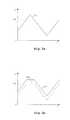
- FIG. 17 shows an ideal diode circuit widely used as limiter circuit.
- An ideal diode circuit 70 includes diodes D 1 , D 2 , D 3 , D 4 , differential amplifiers Q 71 , Q 72 , and resistors R 71 , R 72 .
- FIG. 18 shows an example of operation of the ideal diode circuit 70 .
- an input signal Vin with a waveform as shown in FIG. 18( a ) is applied, and when the input signal Vin is larger than an upper limit threshold signal VH, the diode D 1 becomes ON, the diode D 2 becomes OFF, and voltage Vn 20 at node N 20 becomes equal to VH.
- the diode D 1 becomes OFF, the diode D 2 becomes ON, and voltage Vn 20 at node N 20 becomes equal to the input signal Vin.
- this ideal diode circuit 70 is a limit operation which limits upper and lower limits of the input signal Vin.
- This ideal diode circuit 70 can provide a sufficient limit operation for a signal with a low-speed frequency.
- delays in following the waveform will occur as shown in FIG. 18( c ), under the influence of reverse recovery time of the diodes D 1 , D 2 , D 3 , D 4 and forward voltage drop.
- the output signal Vout is subject to omission periods and periods of output beyond the upper or lower threshold voltages. Thus, it has been impossible to realize adequate limit operation.
- the lower limit threshold signal VL varies with time in the foregoing ideal diode circuit 70
- the lower limit of output signal Vout also varies.
- it is widely practised to identify an incident position by carrying out, with an analog circuit, centroid calculation of radiation signals inputted through numerous channels.
- an application circuit of the foregoing ideal diode circuit is used as a limiter circuit.
- a dynamic threshold signal VL can be used, which is time variable in proportion to the signal level of a radiation signal varying each time.
- the lower limit of output signal Vout of the limiter circuit is required to have a constant value.
- the lower limit of output signal Vout of the above ideal diode circuit 70 will become a dynamic lower limit threshold signal VL. Since the lower limit of output signal Vout varies when the dynamic lower limit threshold signal VL is used, it is necessary to cancel variations in the lower limit of output signal Vout due to the variations of lower limit threshold signal VL. This poses a problem of increasing components of the limiter circuit, thereby complicating the circuit.
- This invention has been made having regard to the state of the art noted above, and its object is to provide limiter circuits having a simple circuit configuration, which can realize a limit operation also with a signal of high-speed frequency.
- this invention provides the following construction.
- a limiter circuit is a limiter circuit to which an input signal voltage, an upper limit threshold signal voltage and a lower limit threshold signal voltage are inputted, comprising an upper limit limiter circuit having a pair of transistors switchable ON and OFF in response to levels of the input signal voltage and the upper limit threshold signal voltage, for cutting voltage components higher than the upper limit threshold signal voltage from the input signal voltage, increasing the input signal voltage, and outputting an upper limit signal voltage; a lower limit threshold correcting circuit for correcting the lower limit threshold signal voltage in accordance with a voltage to which the input signal voltage is increased by the upper limit limiter circuit, and outputting an upper limit threshold correction signal voltage; a lower limit limiter circuit having a different pair of transistors switchable ON and OFF in response to levels of the upper limit signal voltage and the upper limit threshold correction signal voltage, for cutting voltage components lower than the lower limit threshold correction signal voltage from the upper limit signal voltage, decreasing the upper limit signal voltage, and outputting an upper and lower limit signal voltage; a potential correcting circuit for correcting the lower limit threshold correction
- the upper limit limiter circuit includes a pair of first and second PNP transistors having emitter terminals connected to each other, and a first constant current generating device connected between the emitter terminals of the first and second PNP transistors and a first common voltage, the input signal voltage being inputted to a base terminal of the first PNP transistor, the upper limit threshold signal voltage being inputted to a base terminal of the second PNP transistor, the first constant current generating device limiting current flow to the first or second PNP transistor;
- the lower limit threshold correcting circuit includes a third PNP transistor having a base terminal for receiving input of the lower limit threshold signal voltage, and a second constant current generating device connected between an emitter terminal of the third PNP transistor and the first common voltage, the second constant current generating device limiting current flow to the third PNP transistor;
- the lower limit limiter circuit includes a pair of first and second NPN transistors having emitter terminals connected to each other, and a third constant current generating device connected between the emitter terminals of the first
- a limiter circuit is a limiter circuit to which an input signal voltage, an upper limit threshold signal voltage and a lower limit threshold signal voltage are inputted, comprising an upper limit limiter circuit having a pair of transistors switchable ON and OFF in response to levels of the input signal voltage and the upper limit threshold signal voltage, for cutting voltage components higher than the upper limit threshold signal voltage from the input signal voltage, increasing the input signal voltage, and outputting an upper limit signal voltage; a lower limit threshold correcting circuit for correcting the lower limit threshold signal voltage in accordance with a voltage to which the input signal voltage is increased by the upper limit limiter circuit, and outputting an lower limit threshold correction signal voltage; a lower limit limiter circuit having a different pair of transistors switchable ON and OFF in response to levels of the upper limit signal voltage and the lower limit threshold correction signal voltage, for cutting voltage components lower than the lower limit threshold correction signal voltage from the upper limit signal voltage, decreasing the upper limit signal voltage, and outputting an upper and lower limit signal voltage; and an adding and subtracting circuit for generating an output signal voltage
- the upper limit limiter circuit includes a pair of first and second PNP transistors having emitter terminals connected to each other, and a first constant current generating device connected between the emitter terminals of the first and second PNP transistors and a first common voltage, the input signal voltage being inputted to a base terminal of the first PNP transistor, the upper limit threshold signal voltage being inputted to a base terminal of the second PNP transistor, the first constant current generating device limiting current flow to the first or second PNP transistor;
- the lower limit threshold correcting circuit includes a third PNP transistor having a base terminal for receiving input of the lower limit threshold signal voltage, and a second constant current generating device connected between an emitter terminal of the third PNP transistor and the first common voltage, the second constant current generating device limiting current flow to the third PNP transistor;
- the lower limit limiter circuit includes a pair of first and second NPN transistors having emitter terminals connected to each other, and a third constant current generating device connected between the emitter terminals of the first
- a limiter circuit is a limiter circuit to which an input signal voltage and a lower limit threshold signal voltage are inputted, comprising a lower limit limiter circuit having a pair of transistors switchable ON and OFF in response to levels of the input signal voltage and the lower limit threshold correction signal voltage, for decreasing the input signal voltage, and outputting a lower limit signal voltage; a potential correcting circuit for correcting the lower limit threshold signal voltage in accordance with a voltage to which the input signal voltage is decreased by the lower limit limiter circuit, and outputting a first reference signal voltage; and an adding and subtracting circuit for generating an output signal voltage by adding a second reference signal voltage inputted separately, to a signal voltage generated according to a voltage difference between the lower limit signal voltage and the first reference signal voltage; whereby the limiter circuit allows passage of only signal voltage components of the input signal voltage higher than the lower limit threshold signal voltage.
- the lower limit limiter circuit includes a pair of first and second NPN transistors having emitter terminals connected to each other, and a first constant current generating device connected between the emitter terminals of the first and second NPN transistors and a second common voltage, the input signal being connected to a base terminal of the first NPN transistor, the lower limit threshold signal voltage being inputted to a base terminal of the second NPN transistor, the first constant current generating device limiting current flow to the first or second NPN transistor;
- the potential correcting circuit includes a third NPN transistor having a base terminal to which the lower limit threshold signal voltage is inputted, and a second constant current generating device connected between an emitter terminal of the third NPN transistor and the second common voltage, the second constant current generating device limiting current flow to the third NPN transistor; and the adding and subtracting circuit includes a differential amplifier having a positive input node connected with the emitter terminals of the first and second NPN transistors through a first input resistor, and a
- a pair of transistors carry out comparisons between the input signal voltage and threshold signal voltages and line switching at the same time. Therefore, there is no influence of propagation delay. Further, no switching noise occurs at times of line switching.
- a simple circuit construction can carry out a limit operation also with high-speed frequency signals.
- FIG. 1 is a circuit diagram showing a limiter circuit 1 according to Embodiment 1 of this invention.
- FIG. 2 is an explanatory view illustrating operation of a switching circuit 2 according to Embodiment 1 of this invention
- FIG. 3 is an explanatory view illustrating operation of a lower limit threshold correcting circuit 3 according to Embodiment 1 of this invention
- FIG. 4 is an explanatory view illustrating operation of a switching circuit 4 according to Embodiment 1 of this invention.
- FIG. 5 is an explanatory view illustrating operation of a potential correcting circuit 5 according to Embodiment 1 of this invention.
- FIG. 6 is an explanatory view illustrating operation of an adding and subtracting circuit 6 according to Embodiment 1 of this invention.
- FIG. 7 is an explanatory view illustrating operation of the limiter circuit 1 at a time of varying with time a lower limit threshold signal according to Embodiment 1 of this invention
- FIG. 8 is a circuit diagram showing a limiter circuit 10 according to Embodiment 2 of this invention.
- FIG. 9 is an explanatory view illustrating operation of the limiter circuit 10 according to Embodiment 2 of this invention.
- FIG. 10 is a circuit diagram showing a limiter circuit 20 according to Embodiment 3 of this invention.
- FIG. 11 is an explanatory view illustrating operation of the limiter circuit 20 according to Embodiment 3 of this invention.
- FIG. 12 is an explanatory view illustrating operation of the limiter circuit 20 at a time of varying with time a lower limit threshold signal according to Embodiment 3 of this invention.
- FIG. 13 is a circuit diagram showing a limiter circuit according a modification of Embodiment 1 of this invention.
- FIG. 14 is a circuit diagram showing a limiter circuit according to a modification of Embodiment 2 of this invention.
- FIG. 15 is a circuit diagram showing a limiter circuit according to a modification of Embodiment 3 of this invention.
- FIG. 16 is a circuit diagram showing a limiter circuit according to a modification of Embodiment 3 of this invention.
- FIG. 17 is a circuit diagram showing an ideal diode circuit which is a limiter circuit in the prior art.
- FIG. 18 is an explanatory view illustrating operation of the ideal diode circuit in the prior art.
- FIG. 1 is a circuit diagram showing a limiter circuit according to Embodiment 1.
- the limiter circuit of this invention is formed, for example, in an IC, such as an input buffer amplifier of an analog-to-digital converter, or a signal processing circuit.
- a limiter circuit 1 in Embodiment 1 includes a switching circuit 2 for carrying out ON/OFF control in response to a magnitude relation between an input signal Vin and an upper limit threshold signal VH, a lower limit threshold correcting circuit 3 for correcting a potential increased with the switching control of the switching circuit 2 to a lower limit threshold signal VL, a switching circuit 4 for carrying out ON/OFF control in response to a magnitude relation between outputs of the switching circuit 2 and lower limit threshold correcting circuit 3 , a potential correcting circuit 5 for correcting a potential decreased with the switching control of the switching circuit 4 , and an adding and subtracting circuit 6 for carrying out differential amplification of outputs of the switching circuit 4 and potential correcting circuit 5 .
- the input signal Vin corresponds to the input signal voltage in this invention.
- the upper limit threshold signal VH corresponds to the upper limit threshold signal voltage in this invention.
- the lower limit threshold signal VL corresponds to the lower limit threshold signal voltage in this invention.
- the switching circuit 2 corresponds to the upper limit limiter circuit in this invention.
- the switching circuit 4 corresponds to the lower limit limiter circuit in this invention.
- Differential signals are inputted to a pair of PNP transistors Q 1 and Q 2 .
- the base of PNP transistor Q 1 is connected to the input signal Vin.
- the base of PNP transistor Q 2 is connected to the upper limit threshold signal VH.
- the emitters of PNP transistors Q 1 and Q 2 are connected to a node N 1 , while the collectors are connected to ground voltage GND.
- a resistor R 1 is connected between the node N 1 and a positive voltage source Vcc, to function as a constant current source for limiting current flow to the PNP transistors Q 1 and Q 2 .
- the resistor R 1 corresponds to the first constant current generating device in this invention.
- the voltage source Vcc corresponds to the first common voltage in this invention.
- the ground voltage GND corresponds to the second common voltage in this invention.
- FIG. 2( a ) is a view showing a relationship between the input signal Vin and upper limit threshold signal VH inputted to the switching circuit 2 .
- the PNP transistor Q 1 carries out an emitter follower operation. That is, a switching operation takes place to turn on the PNP transistor Q 1 , and turn off the PNP transistor Q 2 .
- Potential Vn 1 at node N 1 becomes a potential having base-emitter voltage Vbep 1 of the PNP transistor Q 1 added to the input signal Vin.
- Vn 1 V in+ Vbep 1 ( V in ⁇ VH ) (1)
- the PNP transistor Q 2 When the input signal Vin is higher than the upper limit threshold signal VH, or when Vin>VH is formed, the PNP transistor Q 2 carries out an emitter follower operation. That is, a switching operation takes place to turn off the PNP transistor Q 1 , and turn on the PNP transistor Q 2 .
- Potential Vn 1 at node N 1 becomes a potential having base-emitter voltage Vbep 2 of the PNP transistor Q 2 added to the upper limit threshold signal VH.
- Vn 1 VH+Vbep 2 ( V in> VH ) (2)
- the base-emitter voltages Vbep 1 and Vbep 2 of PNP transistors Q 1 and Q 2 have substantially the same characteristics since the PNP transistors Q 1 and Q 2 are formed in the same IC.
- the switching circuit 2 carries out a comparison to check whether the input signal Vin inputted is larger or smaller than the upper limit threshold signal VH. And the PNP transistors Q 1 and Q 2 take switching action based on this comparison, and cut signal voltage components exceeding the upper limit threshold signal VH from the input signal Vin. At the same time, the input signal Vin with the upper limit cut off is increased by an amount corresponding to the base-emitter voltage Vbep of PNP transistors Q 1 and Q 2 . In this way, potential Vn 1 shown in FIG. 2( b ) is outputted from the node N 1 . The potential Vn 1 at the node N 1 corresponds to the upper limit signal voltage in this invention.
- the lower limit threshold signal VL is inputted to the base of a PNP transistor Q 3 , with the emitter connected to a node N 2 and the collector connected to ground voltage GND.
- a resistor R 2 is connected between the node N 2 and positive voltage source Vcc to function as a constant current source for limiting current flow to the PNP transistor Q 3 .
- the resistor R 2 corresponds to the second constant current generating device in this invention.
- Vn 2 at the node N 2 is determined by the lower limit threshold signal VL shown in FIG. 3( a ) and a base-emitter voltage Vbep 3 of the PNP transistor Q 3 .
- Vn 2 VL+Vbep 3 (6)
- the PNP transistor Q 3 is also formed in the same IC as the PNP transistors Q 1 and Q 2 , and therefore has substantially the same characteristics.
- Vn 2 VL+Vbep (8)
- the lower limit threshold correcting circuit 3 corrects the lower limit threshold signal VL by increasing the lower limit threshold signal VL also by the same potential difference as the base-emitter voltage Vbep by which the input signal Vin was increased in the switching circuit 2 .
- the potential Vn 2 corrected as shown in FIG. 4( b ) is outputted from the node N 2 .
- the potential Vn 2 at the node N 2 corresponds to the lower limit threshold correction signal voltage in this invention.
- Differential signals (potential Vn 1 from the node N 1 and potential Vn 2 from the node N 2 ) are inputted to a pair of NPN transistors Q 4 and Q 5 .
- the base of NPN transistor Q 4 is connected to the node N 1 .
- the base of NPN transistor Q 5 is connected to the node N 2 .
- the emitters of NPN transistors Q 4 and Q 5 are connected to a node N 3 , while the collectors are connected to the positive voltage source Vcc.
- a resistor R 3 is connected between the node N 3 and ground voltage GND to function as a constant current source for limiting current flow to the NPN transistors Q 4 and Q 5 .
- the resistor R 3 corresponds to the third constant current generating device in this invention.
- the NPN transistor Q 4 carries out an emitter follower operation. That is, a switching operation takes place to turn on the NPN transistor Q 4 and turn off the NPN transistor Q 5 .
- Potential Vn 3 at the node N 3 becomes a potential by subtracting base-emitter voltage Vbep 4 of the NPN transistor Q 4 from the potential Vn 1 of the node N 1 .
- Vn 3 Vn 1 ⁇ Vben 4 ( Vn 1 ⁇ Vn 2) (9)
- the NPN transistor Q 5 When the potential Vn 1 from the node N 1 is lower than the potential Vn 2 from the node N 2 , or when Vn 1 ⁇ Vn 2 is formed, the NPN transistor Q 5 carries out an emitter follower operation. That is, a switching operation takes place to turn off the NPN transistor Q 4 and turn on the NPN transistor Q 5 .
- Potential Vn 3 at node N 3 becomes a potential by subtracting base-emitter voltage Vbep 5 of the NPN transistor Q 5 from the potential Vn 2 of node N 2 .
- Vn 3 Vn 2 ⁇ Vben 5 ( Vn 1 ⁇ Vn 2) (10)
- the base-emitter voltages Vbep 4 and Vbep 5 of NPN transistors Q 4 and Q 5 have substantially the same characteristics since the NPN transistors Q 4 and Q 5 are formed in the same IC.
- the switching circuit 4 carries out a comparison to check whether the inputted potential Vn 1 of node N 1 is larger or smaller than the potential Vn 2 of node N 2 resulting from the correction of the lower limit threshold signal VL. And the NPN transistors Q 4 and Q 5 take switching action based on this comparison, and cut signal voltage components lower than the potential Vn 2 from the potential Vn 1 inputted. At the same time, it is decreased by an amount corresponding the base-emitter voltage Vben of the NPN transistors Q 4 and Q 5 . In this way, potential Vn 3 shown in FIG. 4( b ) is outputted from the node N 3 .
- the potential Vn 3 at the node N 3 corresponds to the upper and lower limit signal voltage in this invention.
- the potential Vn 2 of node N 2 is inputted to the base of an NPN transistor Q 6 , with the emitter connected to a node N 4 , and the collector connected to the positive voltage source Vcc.
- a resistor R 4 is connected between the node N 4 and ground voltage GND to function as a constant current source for limiting current flow to the NPN transistor Q 6 .
- the resistor R 4 corresponds to the fourth constant current generating device in this invention.
- Potential Vn 4 at the node N 4 is determined by the potential Vn 2 of node N 2 shown in FIG. 5( a ) and a base-emitter voltage Vben 6 of the NPN transistor Q 6 .
- Vn 4 Vn 2 ⁇ Vben 6 (14)
- the NPN transistor Q 6 is also formed in the same IC, and therefore has substantially the same characteristics.
- the potential correcting circuit 5 corrects the potential Vn 2 by decreasing the potential Vn 2 outputted from the node N 2 also by the same potential difference as the base-emitter voltage Vben by which the potential Vn 1 of node N 1 was decreased in the switching circuit 4 .
- the potential Vn 4 corrected as shown in FIG. 4( b ) is outputted from the node N 4 .
- the potential Vn 4 at the node N 4 corresponds to the first reference signal voltage in this invention.
- the node N 3 is connected to a positive input node of a differential amplifier Q 7 through a resistor R 5 , while the node N 4 is connected to a negative input node through a resistor R 6 .
- a reference voltage Vref 2 is inputted to the positive input node through a resistor R 8 .
- the negative input node and an output node are connected through a resistor R 7 to provide a negative feedback.
- the reference voltage Vref 2 corresponds to the second reference signal voltage in this invention.
- Output signal Vout of the differential amplifier Q 7 is determined by the potential Vn 3 of node N 3 and the potential Vn 4 of node N 4 shown in FIG. 6( a ), the reference voltage Vref 2 , and the resistors R 5 , R 6 , R 7 and R 8 .
- the output signal Vout corresponds to the output signal voltage in this invention.
- the amplification factor by the differential amplifier Q 7 is determined by a relationship between R and R 7 .
- V out Vn 3 ⁇ Vn 4+ V ref2 (21)
- output signal Vout when the input signal Vin is higher than the upper limit threshold signal VH is as follows from equation (5), equation (8), equation (12), equation (16) and equation (21):
- Vref 2 has a constant value, as shown in FIG. 6( d ), the lower limit of the output signal Vout becomes the value of Vref 2 .
- the adding and subtracting circuit 6 subtracts the potential Vn 4 of node N 4 inputted to the negative input node from the potential Vn 3 of node N 3 inputted to the positive input node, and adds the reference voltage Vref 2 .
- voltage components higher than the upper limit threshold signal VH and voltage components lower than the lower limit threshold signal VL can be removed from the input signal Vin, and a voltage signal with a lower limit corresponding to the reference voltage Vref 2 can be outputted.
- the switching circuit 2 cuts signal voltage components exceeding the upper limit threshold signal VH from the input signal Vin.
- the input signal Vin with the upper limit cut off is increased by an amount corresponding to the base-emitter voltage Vbep of the PNP transistors Q 1 and Q 2 .
- potential Vn 1 shown in FIG. 7( b ) is outputted from the node N 1 .
- the lower limit threshold correcting circuit 3 carries out a correction to increase the lower limit threshold signal VL by an amount corresponding to the base-emitter voltage Vbep of the PNP transistor Q 3 , and outputs potential Vn 2 from the node N 2 .
- the switching circuit 4 cuts signal voltage components lower than the potential Vn 2 from the potential Vn 1 .
- the voltage is decreased by an amount corresponding to the base-emitter voltage Vben of the NPN transistors Q 4 and Q 5 .
- potential Vn 3 shown in FIG. 7( c ) is outputted from the node N 3 .
- the potential correcting circuit 4 carries out a correction to decrease the potential Vn 2 by an amount corresponding to the base-emitter voltage Vben of the NPN transistor Q 6 , and outputs Vn 4 from the node N 4 .
- the adding and subtracting circuit 6 subtracts the potential Vn 4 of node N 4 inputted to the negative input node from the potential Vn 3 of node N 3 inputted to the positive input node, and adds the reference voltage Vref 2 .
- the lower limit threshold signal VL varies with time, as shown in FIG. 7( d )
- the lower limit of output signal Vout is Vref 2 , which realizes a limit operation not influenced by the temporal variation of the lower limit threshold signal VL.
- a pair of PNP transistors or NPN transistors carry out comparisons between the input signal voltage and threshold signal voltages and line switching at the same time. Therefore, compared with a circuit which carries out comparison using comparators, there is no influence of propagation delay and no switching noise occurs at times of line switching.
- the limiter circuit can be made to have little variation in characteristics and to be highly precise. Since the application frequency band of limit operation depends on the frequency characteristics of the transistors used, a limit operation with signals with a high-speed frequency of several MHz or more, for example, can be realized easily by using high-speed transistors.
- the limiter circuit in Embodiment 1 removes variations of the lower limit even when a dynamic lower limit threshold signal varying with time is inputted, thereby being capable of outputting an output signal with a constant lower limit.
- the limiter circuit in Embodiment 1 automatically corrects, in the lower limit threshold correcting circuit 3 and potential correcting circuit 5 , the voltage increase and decrease by the base-emitter voltages of the PNP transistors and NPN transistors. Therefore, the limiter circuit 1 is operable also when the values of the base-emitter voltages of the PNP transistors and NPN transistors are unknown.
- Embodiment 2 of this invention will be described in detail with reference to FIGS. 8 and 9 .
- FIG. 8 is a circuit diagram showing a limiter circuit according to Embodiment 2.
- FIG. 9 is an explanatory view illustrating operation of the limiter circuit according to Embodiment 2.
- a limiter circuit 10 in Embodiment 2 includes a switching circuit 2 for carrying out ON/OFF control in response to a magnitude relation between an input signal Vin and an upper limit threshold signal VH, a lower limit threshold correcting circuit 3 for generating a potential for correcting a potential increased with the switching control of the switching circuit 2 to a lower limit threshold signal VL, a switching circuit 4 for carrying out ON/OFF control in response to a magnitude relation between outputs of the switching circuit 2 and lower limit threshold correcting circuit 3 , and an adding and subtracting circuit 11 for carrying out differential amplification of output of the switching circuit 4 and a reference voltage Vref 1 .
- the limiter circuit 10 in Embodiment 2 is a circuit which dispenses with the potential correcting circuit 5 of the limiter circuit 1 in Embodiment 1, and employs the reference voltage Vref 1 instead. Consequently, the constructions and operations of the switching circuit 2 , lower limit threshold correcting circuit 3 and switching circuit 4 of the limiter circuit 10 in Embodiment 2 are the same as in Embodiment 1, and will not be described.
- the node N 3 is connected to a positive input node of a differential amplifier Q 7 through a resistor R 5 .
- the reference voltage Vref 2 is connected to the positive input node through a resistor R 8 , and the reference voltage Vref 1 is inputted to a negative input node through a resistor R 6 .
- the negative input node and an output node are connected through a resistor R 7 to provide a negative feedback.
- the reference voltage Vref 1 corresponds to the first reference signal voltage in this invention.
- the reference voltage Vref 2 corresponds to the second reference signal voltage in this invention.
- Output signal Vout of the differential amplifier Q 7 is determined by the potential Vn 3 of node N 3 , the reference voltages Vref 1 and Vref 2 , and the resistors R 5 , R 6 , R 7 and R 8 .
- the amplification factor by the differential amplifier Q 7 is determined by a relationship between R and R 7 .
- V out Vn 3 ⁇ V ref1+ V ref2 (33)
- FIG. 9( a ) shows a relationship between the input signal Vin, upper limit threshold signal VH and lower limit threshold signal VL inputted to the limiter circuit 10 .
- the switching circuit 2 cuts components of the input signal Vin exceeding the upper limit threshold signal VH, increases it by an amount corresponding to the base-emitter voltage Vbep of PNP transistors Q 1 and Q 2 , and outputs potential Vn 1 from the node N 1 .
- the lower limit threshold correcting circuit 3 increases the lower limit threshold signal VL also by the same potential difference as the base-emitter voltage Vbep by which the input signal Vin was increased in the switching circuit 2 .
- the switching circuit 4 cuts signal voltage components lower than the potential Vn 2 from the potential Vn 1 , and further outputs from the node N 3 the potential Vn 3 decreased by an amount corresponding the base-emitter voltage Vben of NPN transistors Q 4 and Q 5 .
- the output signal Vout outputted from the adding and subtracting circuit 11 when the input signal Vin is higher than the upper limit threshold signal VH (Vin>VH) is as follows:
- VH upper limit threshold signal
- VL lower limit threshold signal
- Vout VL (41), thereby realizing a limit operation.
- Vref 2 has a constant value
- the lower limit of the output signal Vout becomes the value of Vref 2 as shown in FIG. 9( d ).
- Vout VH (44).
- Vout Vin (45).
- Vout VL (46).
- the lower limit of the output signal Vout of the adding and subtracting circuit 9 is as follows: VL+Vbep ⁇ Vben ⁇ V ref1+ V ref2 (47)
- V ref1 VL+Vbep ⁇ Vben (48)
- the lower limit of the output signal Vout is determined by Vref 2 , which realizes a limit operation not influenced by the lower limit threshold signal VL.
- a pair of PNP transistors or NPN transistors carry out comparisons between the input signal voltage and threshold signal voltages and line switching at the same time. Therefore, compared with a circuit which carries out comparison using comparators, there is no influence of propagation delay and no switching noise occurs at times of line switching.
- the limiter circuit can be made to have little variation in characteristics and to be highly precise. Since the application frequency band of limit operation depends on the frequency characteristics of the transistors used, a limit operation with signals with a high-speed frequency of several MHz or more, for example, can be realized easily by using high-speed transistors.
- the limiter circuit 10 in Embodiment 2 removes variations of the lower limit even when a dynamic lower limit threshold signal varying with time is inputted, thereby being capable of outputting an output signal with a constant lower limit.
- FIG. 10 is a circuit diagram showing a limiter circuit according to Embodiment 3.
- FIG. 11 is an explanatory view illustrating operation of the limiter circuit according to Embodiment 3.
- a limiter circuit 20 in Embodiment 3 includes a switching circuit 21 for carrying out ON/OFF control in response to a magnitude relation between an input signal Vin and a lower limit threshold signal VL, a potential correcting circuit 22 for correcting a potential decreased by the switching circuit 21 , and an adding and subtracting circuit 23 for carrying out differential amplification of outputs of the switching circuit 21 and potential correcting circuit 21 .
- the switching circuit 21 corresponds to the lower limit limiter circuit in this invention.
- the limiter circuit 20 in Embodiment 3 carries out only a lower limit operation, and is a circuit omitting the switching circuit 2 and lower limit threshold correcting circuit 3 from the limiter circuit 1 in Embodiment 1.
- Differential signals are inputted to a pair of NPN transistors Q 4 and Q 5 .
- the base of NPN transistor Q 4 is connected to the input signal Vin.
- the base of NPN transistor Q 5 is connected to the lower limit threshold signal VL.
- the emitters of NPN transistors Q 4 and Q 5 are connected to a node N 5 , while the collectors are connected to a positive voltage source Vcc.
- a resistor R 9 is connected between the node N 5 and ground voltage GND to function as a constant current source for limiting current flow to the NPN transistors Q 4 and Q 5 .
- the resistor R 9 corresponds to the first constant current generating device in this invention.
- the ground voltage GND corresponds to the second common voltage in this invention.
- the NPN transistor Q 4 carries out an emitter follower operation. That is, a switching operation takes place to turn on the NPN transistor Q 4 and turn off the NPN transistor Q 5 .
- Potential Vn 5 at node N 5 becomes a potential by subtracting base-emitter voltage Vben 4 of the NPN transistor Q 4 from the input signal Vin.
- Vn 5 V in ⁇ Vben 4 ( V in ⁇ VL ) (49)
- the NPN transistor Q 5 When the input signal Vin is lower than the lower limit threshold signal VL, or when Vin ⁇ VL is formed, the NPN transistor Q 5 carries out an emitter follower operation. That is, a switching operation takes place to turn off the NPN transistor Q 4 and turn on the NPN transistor Q 5 .
- Potential Vn 5 at node N 5 becomes a potential by subtracting base-emitter voltage Vben 5 of the NPN transistor Q 5 from the lower limit threshold signal VL.
- Vn 5 VL ⁇ Vben 5 ( V in ⁇ VL ) (50)
- the base-emitter voltages Vbep 4 and Vbep 5 of NPN transistors Q 4 and Q 5 have substantially the same characteristics since the NPN transistors Q 4 and Q 5 are formed in the same IC.
- Vn 5 V in ⁇ Vben ( V in ⁇ VL ) (52)
- Vn 5 VL ⁇ Vben ( V in ⁇ VL ) (53)
- the switching circuit 21 carries out a comparison to check whether the input signal Vin inputted is larger or smaller than the lower limit threshold signal VL. And the NPN transistors Q 4 and Q 5 take switching action based on this comparison, and cut signal voltage components lower than the lower limit threshold signal VL from the input signal Vin. At the same time, it is decreased by an amount corresponding the base-emitter voltage Vben of NPN transistors Q 4 and Q 5 . In this way, potential Vn 5 shown in FIG. 11( b ) is outputted from the node N 5 . The potential Vn 5 at the node N 5 corresponds to the lower limit signal voltage in this invention.
- the lower limit threshold signal VL is inputted to the base of an NPN transistor Q 6 , with the emitter connected to a node N 6 , and the collector connected to the positive voltage source Vcc.
- a resistor R 6 is connected between the node N 6 and ground voltage GND, and functions as a constant current source for limiting current flow to the NPN transistor Q 6 .
- the resistor R 6 corresponds to the second constant current generating device in this invention.
- Vn 6 at the node N 6 is determined by the lower limit threshold signal VL and a base-emitter voltage Vben 6 of the NPN transistor Q 6 .
- Vn 6 VL ⁇ Vben 6 (54)
- the NPN transistor Q 6 is also formed in the same IC, and therefore has substantially the same characteristics.
- the potential correcting circuit 22 corrects the lower limit threshold signal VL by decreasing the lower limit threshold signal VL also by the same potential difference as the base-emitter voltage Vben by which the input signal Vin was decreased in the switching circuit 21 .
- the potential Vn 6 corrected as shown in FIG. 11( b ) is outputted from the node N 6 .
- the potential Vn 6 at the node N 6 corresponds to the first reference signal voltage in this invention.
- the node N 5 is connected to a positive input node of a differential amplifier Q 7 through a resistor R 5 , while the node N 6 is connected to a negative input node through a resistor R 6 .
- a reference voltage Vref 2 is connected to the positive input node through a resistor R 8 .
- the negative input node and an output node are connected through a resistor R 7 to provide a negative feedback.
- the reference voltage Vref 2 corresponds to the second reference signal voltage in this invention.
- Output signal Vout of the differential amplifier Q 7 is determined by the potential Vn 5 of node N 5 and the potential Vn 6 of node N 6 , the reference voltage Vref 2 , and the resistors R 5 , R 6 , R 7 and R 8 .
- the amplification factor is determined by a relationship between R and R 7 .
- V out Vn 5 ⁇ Vn 6+ V ref2 (61)
- VL the lower limit threshold signal
- V out V in ( V in ⁇ VL ) (65)
- V out VL ( V in ⁇ VL ) (66)
- the adding and subtracting circuit 23 subtracts the potential Vn 6 of node N 6 inputted to the negative input node from the potential Vn 5 of node N 5 inputted to the positive input node, and adds the reference voltage Vref 2 .
- voltage components lower than the lower limit threshold signal VL can be removed from the input signal Vin, and a voltage signal with a lower limit corresponding to the reference voltage Vref 2 can be outputted.
- the switching circuit 21 cuts signal voltage components lower than the lower limit threshold signal VL from the input signal Vin. At the same time, the voltage is decreased by an amount corresponding to the base-emitter voltage Vben of the NPN transistors Q 4 and Q 5 . In this way, potential Vn 5 shown in FIG. 12( c ) is outputted from the node N 5 . Similarly, the potential correcting circuit 4 outputs from the node N 6 the potential Vn 6 resulting from the correction to decrease the lower limit threshold signal VL by an amount corresponding to the base-emitter voltage Vben of the NPN transistor Q 6 .
- the adding and subtracting circuit 23 subtracts the potential Vn 6 of node N 6 inputted to the negative input node from the potential Vn 5 of node N 5 inputted to the positive input node, and adds the reference voltage Vref 2 .
- the lower limit threshold signal VL varies with time, as shown in FIG. 12( c )
- the lower limit of output signal Vout is Vref 2 , which realizes a limit operation not influenced by the lower limit threshold signal VL.
- a pair of NPN transistors carry out comparisons between the input signal voltage and threshold signal voltages and line switching at the same time. Therefore, compared with a circuit which carries out comparison using comparators, there is no influence of propagation delay and no switching noise occurs at times of line switching.
- the limiter circuit 20 of Embodiment 3 can be arranged close together in the same chip, the limiter circuit can be made to have little variation in characteristics and to be highly precise. Since the application frequency band of limit operation depends on the frequency characteristics of the transistors used, a limit operation with signals with a high-speed frequency of several MHz or more, such as video signals, for example, can be realized easily by using high-speed transistors.
- the limiter circuit 20 in Embodiment 3 removes variations of the lower limit even when a dynamic lower limit threshold signal varying with time is inputted, thereby being capable of outputting an output signal with a constant lower limit.
- the limiter circuit 20 in Embodiment 3 automatically corrects, in the potential correcting circuit 22 , the voltage decrease by the base-emitter voltage of the NPN transistors. Therefore, the limiter circuit 20 is operable also when the value of the base-emitter voltage of the NPN transistors is unknown.
- the lower limit of the output signal Vout outputted from the limiter circuits is determined by Vref 2 .
- Vref 2 a level shift of the output signal Vout can be carried out at the same time by adjusting Vref 2 . Consequently, even when the output signal Vout is connected to an analog-to-digital converter of single power source, the limiter circuit can carry out a limit operation and level shift for the input signal Vin for adjustment to the input range of the analog-to-digital converter.
- ground voltage GND is given as Vref 2
- the lower limit of output signal Vout will become ground voltage GND.
- Embodiments 1-3 Only elements that can be constructed in a standard semiconductor process are used in Embodiments 1-3. Since the number of elements used is relatively small, a low occupying area is realizable, and the limiter circuit can be made at low cost. This can be realized easily in a standard process for semiconductor integrated circuits, and speed-up can be realized easily. Since it is realizable only by adding relatively simple elements to the adding and subtracting circuit, miniaturization of ICs can be achieved easily.
- Embodiment 1 described hereinbefore shows the construction of an upper and lower limit limiter circuit which gives a constant lower limit to the output signal Vout when outputting a lower limit threshold signal which is fixed or varies with time.
- an upper and lower limit limiter circuit may be modified to give a constant upper limit to the output signal Vout when outputting an upper limit threshold signal which is fixed or varies with time.
- the limiter circuit 30 has the following construction. It includes a lower limit limiter circuit 31 having a pair of transistors Q 4 and Q 5 switchable ON and OFF in response to levels of an input signal voltage Vin and a lower limit threshold signal voltage VL, for cutting voltage components lower than the lower limit threshold signal voltage VL from the input signal voltage Vin, decreasing the input signal voltage Vin, and outputting a lower limit signal voltage Vn 7 from a node N 7 ; an upper limit threshold correcting circuit 32 for correcting an upper limit threshold signal voltage VH in accordance with a voltage to which the input signal Vin is decreased by the lower limit limiter circuit 31 , and outputting an upper limit threshold correction signal voltage Vn 8 from a node N 8 ; an upper limit limiter circuit 33 having a different pair of transistors Q 1 and Q 2 switchable ON and OFF in response to levels of the lower limit signal voltage Vn 7 and the upper limit threshold correction signal voltage Vn 8 , for cutting voltage components higher than the upper limit threshold correction signal voltage Vn 8 from the lower limit signal
- Embodiment 2 described hereinbefore shows the construction of an upper and lower limit limiter circuit which omits the potential correcting circuit 5 from the limiter circuit 1 in the first embodiment.
- a limiter circuit 40 may be provided which omits the lower limit threshold correcting circuits 3 instead of omitting the potential correcting circuits 5 .
- Both the potential correcting circuit 5 and lower limit threshold correcting circuits 3 of foregoing Embodiment 1 may be omitted, and instead, a third reference voltage may be applied to the adding and subtracting circuit 11 .
- the limiter circuit 40 has the following construction. It includes a lower limit limiter circuit 41 having a pair of transistors Q 4 and Q 5 switchable ON and OFF in response to levels of an input signal voltage Vin and a lower limit threshold signal voltage VL, for cutting voltage components lower than the lower limit threshold signal voltage VL from the input signal voltage Vin, decreasing the input signal voltage Vin, and outputting a lower limit signal voltage Vn 11 from a node N 11 ; an upper limit threshold correcting circuit 42 for correcting an upper limit threshold signal voltage VH in accordance with a voltage to which the input signal voltage Vin is decreased by the lower limit limiter circuit 41 , and outputting an upper limit threshold correction signal voltage Vn 12 from a node N 12 ; an upper limit limiter circuit 43 having a different pair of transistors Q 1 and Q 2 switchable ON and OFF in response to levels of the lower limit signal voltage Vn 11 and the upper limit threshold correction signal voltage Vn 12 , for cutting voltage components higher than the upper limit threshold correction signal voltage Vn 12 from the lower limit
- Embodiment 3 described hereinbefore shows the construction of a lower limit limiter circuit which gives a constant lower limit to the output signal Vout at the time of application of a lower limit threshold signal which is fixed or varies with time.
- a limiter circuit 50 may be provided which gives a constant upper limit to the output signal Vout at the time of application of an upper limit threshold signal which is fixed or varies with time.
- the limiter circuit 50 has the following construction. It includes an upper limit limiter circuit 51 having a pair of transistors Q 1 and Q 2 switchable ON and OFF in response to levels of an input signal voltage Vin and an upper limit threshold signal voltage VH, increasing the input signal voltage Vin, and outputting an upper limit signal voltage Vn 14 from a node N 14 ; an upper limit threshold correcting circuit 52 for correcting the upper limit threshold signal voltage VH in accordance with a voltage to which the input signal voltage Vin is increased by the upper limit limiter circuit 51 , and outputting a first reference signal voltage Vn 15 from a node N 15 ; and an adding and subtracting circuit 53 for generating an output signal voltage Vout by adding a second reference signal voltage Vref 2 inputted separately, to a signal voltage generated according to a voltage difference between the upper limit signal voltage Vn 14 and the first reference signal voltage Vn 15 .
- an upper limit limiter circuit 51 having a pair of transistors Q 1 and Q 2 switchable ON and OFF in response to levels of an input signal voltage Vin and an
- a limiter circuit 60 may be formed by combining both the limiter circuit 20 and limiter circuit 50 , to carry out an upper and lower limiter operation.
- This limiter circuit 60 is capable of a limit operation to provide a constant upper limit and lower limit also when both the upper limit threshold signal and lower limit threshold signal vary with time.
- the limiter circuit 60 has the following construction. It includes an upper limit limiter circuit 61 having a pair of transistors Q 1 and Q 2 switchable ON and OFF in response to levels of an input signal voltage Vin and an upper limit threshold signal voltage VH, increasing the input signal voltage Vin, and outputting an upper limit signal voltage Vn 16 from a node N 16 ; an upper limit threshold correcting circuit 62 for correcting the upper limit threshold signal voltage VH in accordance with a voltage to which the input signal voltage Vin is increased by the upper limit limiter circuit 61 , and outputting a first reference signal voltage Vn 17 from a node N 17 ; an adding and subtracting circuit 63 for generating an upper limit correction signal voltage by adding a second reference signal voltage Vref 2 inputted separately, to a signal voltage generated according to a voltage difference between the upper limit signal voltage Vn 16 and the first reference signal voltage Vn 17 ; a lower limit limiter circuit 64 having a pair of transistors Q 4 and Q 5 switchable ON and OFF in response to levels of the upper limit correction signal
- the foregoing embodiments use the resistors as constant current sources.
- the constant current sources may be formed of active elements such as transistors.
- the foregoing embodiments use positive voltage source Vcc and ground voltage GND.
- a negative voltage source may be used instead of ground voltage GND.
- the positive voltage source Vcc and ground voltage GND may be replaced with a plurality of voltage sources with a potential difference, such as two positive voltage sources with a potential difference.
- the foregoing embodiments show the constructions of noninversion type limiter circuits.
- the limiter circuits may be used as the inversion type by changing connection to the adding and subtracting circuits.
- the foregoing embodiments use the bipolar transistors (PNP or NPN transistors). It is possible to use various known transistor elements, such as MOS transistors and MIS transistors.
Landscapes
- Tone Control, Compression And Expansion, Limiting Amplitude (AREA)
- Amplifiers (AREA)
- Electronic Switches (AREA)
Abstract
Description
Vn1=Vin+Vbep1 (Vin≦VH) (1)
Vn1=VH+Vbep2 (Vin>VH) (2)
Vbep1=Vbep2=Vbep (3)
Vn1=Vin+Vbep (Vin≦VH) (4)
Vn1=VH+Vbep (Vin>VH) (5)
Vn2=VL+Vbep3 (6)
Vbep3=Vbep1=Vbep2=Vbep (7)
Vn2=VL+Vbep (8)
Vn3=Vn1−Vben4 (Vn1≦Vn2) (9)
Vn3=Vn2−Vben5 (Vn1<Vn2) (10)
Vben4=Vben5=Vben (11)
Vn3=Vn1−Vben (Vn1≦Vn2) (12)
Vn3=Vn2−Vben (Vn1<Vn2) (13)
Vn4=Vn2−Vben6 (14)
Vben6=Vben4=Vben5=Vben (15)
Vn4=Vn2−Vben (16)
Vout=R5×R8/(R5+R8)×(R6+R7)/R6×(Vn3/R5−Vn4/R6+Vref2/R8) (17)
If
R5=R6=R8=R (18),
then
Vout=½×(1+R7/×(Vn3−Vn4+Vref2) (19)
R7=R (20),
then
Vout=Vn3−Vn4+Vref2 (21)
Vref2=VL (25),
Vout=VH (26),
Vout=Vin (27)
Vout=VL (28),
Vout=R5×R8/(R5+R8)×(R6+R7)/R6'(Vn3/R5−Vref1/R6+Vref2/R8) (29)
If
R5=R6=R8=R (30),
then
Vout=½×(1+R7/R)×(Vn3−Vref1+Vref2) (31)
R7=R (32),
then
Vout=Vn3−Vref1+Vref2 (33)
When the input signal Vin is between the upper limit threshold signal VH and lower limit threshold signal VL (VL≦Vin≦VH), the following is formed:
Vref1=Vbep−Vben (37)
and
Vref2=0 (38),
Vout=VH (39),
Vout=Vin (40)
Vout=VL (41),
thereby realizing a limit operation. When Vref2 has a constant value, the lower limit of the output signal Vout becomes the value of Vref2 as shown in
Vbep=Vben (42)
Vref1=Vref2=0 (43),
Vout=VH (44).
Vout=Vin (45).
Vout=VL (46).
VL+Vbep−Vben−Vref1+Vref2 (47)
Vref1=VL+Vbep−Vben (48)
Vn5=Vin−Vben4 (Vin≧VL) (49)
Vn5=VL−Vben5 (Vin<VL) (50)
Vben4=Vben5=Vben (51)
Vn5=Vin−Vben (Vin≧VL) (52)
Vn5=VL−Vben (Vin<VL) (53)
Vn6=VL−Vben6 (54)
Vben6=Vben4=Vben5=Vben (55)
Vn6=VL−Vben (56)
Vout=R5×R8/(R5+R8)×(R6+R7)/R6×(Vn5/R5−Vn6/R6+Vref2/R8) (57)
If
R5=R6=R8=R (58),
then
Vout=½×(1+R7/R)×(Vn5−Vn6+Vref2) (59)
R7=R (60),
then
Vout=Vn5−Vn6+Vref2 (61)
When the input signal Vin is lower than the lower limit threshold signal VL (Vin<VL), the following is formed:
Vref2=VL (64)
Vout=Vin (Vin≧VL) (65)
Vout=VL (Vin<VL) (66),
Claims (13)
Applications Claiming Priority (1)
| Application Number | Priority Date | Filing Date | Title |
|---|---|---|---|
| PCT/JP2008/060566 WO2009150709A1 (en) | 2008-06-09 | 2008-06-09 | Limiter circuit |
Publications (2)
| Publication Number | Publication Date |
|---|---|
| US20110089989A1 US20110089989A1 (en) | 2011-04-21 |
| US8330520B2 true US8330520B2 (en) | 2012-12-11 |
Family
ID=41416434
Family Applications (1)
| Application Number | Title | Priority Date | Filing Date |
|---|---|---|---|
| US12/996,636 Expired - Fee Related US8330520B2 (en) | 2008-06-09 | 2008-06-09 | Limiter circuit |
Country Status (5)
| Country | Link |
|---|---|
| US (1) | US8330520B2 (en) |
| EP (1) | EP2296271B1 (en) |
| JP (1) | JP5168354B2 (en) |
| CN (1) | CN102057569B (en) |
| WO (1) | WO2009150709A1 (en) |
Families Citing this family (7)
| Publication number | Priority date | Publication date | Assignee | Title |
|---|---|---|---|---|
| US9124084B2 (en) | 2011-11-03 | 2015-09-01 | Intel Corporation | Charge injection and drain-based electrical overstress (EOS) protection apparatus and method |
| CN103269206B (en) * | 2013-05-28 | 2016-08-24 | 上海贝岭股份有限公司 | A kind of output limiter circuit of amplifier |
| CN103440010B (en) * | 2013-08-27 | 2015-01-07 | 电子科技大学 | Active voltage limiting circuit |
| CN103699929B (en) * | 2014-01-08 | 2017-01-04 | 卓捷创芯科技(深圳)有限公司 | The rectification that a kind of switching signal controls and amplitude limiter circuit and passive RF label |
| US9696738B2 (en) * | 2014-12-24 | 2017-07-04 | Texas Instruments Incorporated | Low power ideal diode control circuit |
| WO2017059880A1 (en) * | 2015-10-05 | 2017-04-13 | Telefonaktiebolaget Lm Ericsson (Publ) | Amplification device incorporating limiting |
| CN117055441B (en) * | 2023-09-21 | 2024-07-19 | 江苏神州半导体科技有限公司 | A voltage limiting circuit used in FPGA control system |
Citations (1)
| Publication number | Priority date | Publication date | Assignee | Title |
|---|---|---|---|---|
| US7368981B2 (en) * | 2000-12-22 | 2008-05-06 | Niigata Seimitsu Co., Ltd. | Limit circuit |
Family Cites Families (5)
| Publication number | Priority date | Publication date | Assignee | Title |
|---|---|---|---|---|
| JPS6084004A (en) * | 1983-10-14 | 1985-05-13 | Mitsubishi Electric Corp | Amplitude limit circuit |
| JPH03121603A (en) * | 1989-10-04 | 1991-05-23 | Nec Ic Microcomput Syst Ltd | Differential amplifier |
| JPH05160650A (en) * | 1991-02-26 | 1993-06-25 | Mitsubishi Denki Eng Kk | Amplifier circuit with clip |
| JPH0670243A (en) * | 1992-08-18 | 1994-03-11 | Sony Corp | Video switch circuit |
| JP2006270874A (en) * | 2005-03-25 | 2006-10-05 | Nec Corp | Electric power clipping circuit |
-
2008
- 2008-06-09 EP EP08765356.4A patent/EP2296271B1/en not_active Not-in-force
- 2008-06-09 CN CN2008801297215A patent/CN102057569B/en not_active Expired - Fee Related
- 2008-06-09 WO PCT/JP2008/060566 patent/WO2009150709A1/en not_active Ceased
- 2008-06-09 JP JP2010516670A patent/JP5168354B2/en active Active
- 2008-06-09 US US12/996,636 patent/US8330520B2/en not_active Expired - Fee Related
Patent Citations (1)
| Publication number | Priority date | Publication date | Assignee | Title |
|---|---|---|---|---|
| US7368981B2 (en) * | 2000-12-22 | 2008-05-06 | Niigata Seimitsu Co., Ltd. | Limit circuit |
Also Published As
| Publication number | Publication date |
|---|---|
| EP2296271A1 (en) | 2011-03-16 |
| EP2296271A4 (en) | 2013-11-20 |
| WO2009150709A1 (en) | 2009-12-17 |
| CN102057569A (en) | 2011-05-11 |
| EP2296271B1 (en) | 2015-08-12 |
| US20110089989A1 (en) | 2011-04-21 |
| JP5168354B2 (en) | 2013-03-21 |
| JPWO2009150709A1 (en) | 2011-11-04 |
| CN102057569B (en) | 2013-12-18 |
Similar Documents
| Publication | Publication Date | Title |
|---|---|---|
| US8330520B2 (en) | Limiter circuit | |
| US7663089B2 (en) | Receiving apparatus | |
| US6864751B1 (en) | Transimpedance amplifier with adjustable output amplitude and wide input dynamic-range | |
| US7763838B2 (en) | Photodetecting circuit having adder for photodetection | |
| US8952745B2 (en) | Temperature detecting circuit, temperature compensating circuit, and buffer circuit | |
| US11799288B2 (en) | Electrostatic protection circuit and semiconductor integrated circuit | |
| JP6271372B2 (en) | Optical receiving circuit and optical coupling device | |
| US9503119B2 (en) | Common mode sampling mechanism for residue amplifier in switched current pipeline analog-to-digital converters | |
| US9837969B2 (en) | Transimpedance circuit | |
| EP2498052B1 (en) | High-linearity signal-processing amplifier | |
| US7502569B2 (en) | Optical receiver preamplifier | |
| WO2020210145A1 (en) | Peak detector | |
| US11901870B2 (en) | Amplifier | |
| EP1357664A2 (en) | Variable gain amplifer | |
| US4904860A (en) | Optical signal detection circuit with constant current sources | |
| TW202139600A (en) | Peak-detector circuit and method for evaluating a peak of a first input voltage | |
| JP2001168374A (en) | Photoelectric conversion circuit | |
| JP4799051B2 (en) | Semiconductor circuit | |
| US12476597B2 (en) | Amplifier circuit | |
| JP2000068947A (en) | Semiconductor integrated circuit for light reception | |
| JPH0348522A (en) | Optical receiver circuit | |
| JP2005251974A (en) | Optical logic element | |
| CN115833764A (en) | Front-end amplifier circuit and photoelectric system | |
| JPH09116435A (en) | Ad conversion circuit | |
| JP2009038674A (en) | Amplifier circuit |
Legal Events
| Date | Code | Title | Description |
|---|---|---|---|
| AS | Assignment |
Owner name: SHIMADZU CORPORATION, JAPAN Free format text: ASSIGNMENT OF ASSIGNORS INTEREST;ASSIGNORS:FURUMIYA, TETSUO;OHI, JUNICHI;REEL/FRAME:025459/0331 Effective date: 20101115 |
|
| FEPP | Fee payment procedure |
Free format text: PAYOR NUMBER ASSIGNED (ORIGINAL EVENT CODE: ASPN); ENTITY STATUS OF PATENT OWNER: LARGE ENTITY |
|
| CC | Certificate of correction | ||
| REMI | Maintenance fee reminder mailed | ||
| LAPS | Lapse for failure to pay maintenance fees | ||
| STCH | Information on status: patent discontinuation |
Free format text: PATENT EXPIRED DUE TO NONPAYMENT OF MAINTENANCE FEES UNDER 37 CFR 1.362 |
|
| STCH | Information on status: patent discontinuation |
Free format text: PATENT EXPIRED DUE TO NONPAYMENT OF MAINTENANCE FEES UNDER 37 CFR 1.362 |
|
| FP | Lapsed due to failure to pay maintenance fee |
Effective date: 20161211 |