US8330372B2 - Slow wave structures using twisted waveguides for charged particle applications - Google Patents

Slow wave structures using twisted waveguides for charged particle applications Download PDF

Info

Publication number
US8330372B2
US8330372B2 US12/784,571 US78457110A US8330372B2 US 8330372 B2 US8330372 B2 US 8330372B2 US 78457110 A US78457110 A US 78457110A US 8330372 B2 US8330372 B2 US 8330372B2
Authority
US
United States
Prior art keywords
central axis
helical
channel
waveguide
waveguide structure
Prior art date
Legal status (The legal status is an assumption and is not a legal conclusion. Google has not performed a legal analysis and makes no representation as to the accuracy of the status listed.)
Active, expires
Application number
US12/784,571
Other versions
US20110285479A1 (en
Inventor
Yoon W. Kang
Aly E. Fathy
Joshua L. WILSON
Current Assignee (The listed assignees may be inaccurate. Google has not performed a legal analysis and makes no representation or warranty as to the accuracy of the list.)
UT Battelle LLC
University of Tennessee Research Foundation
Original Assignee
UT Battelle LLC
Priority date (The priority date is an assumption and is not a legal conclusion. Google has not performed a legal analysis and makes no representation as to the accuracy of the date listed.)
Filing date
Publication date
Application filed by UT Battelle LLC filed Critical UT Battelle LLC
Priority to US12/784,571 priority Critical patent/US8330372B2/en
Assigned to UNIVERSITY OF TENNESSEE RESEARCH FOUNDATION reassignment UNIVERSITY OF TENNESSEE RESEARCH FOUNDATION ASSIGNMENT OF ASSIGNORS INTEREST (SEE DOCUMENT FOR DETAILS). Assignors: WILSON, JOSHUA L., FATHY, ALY E.
Assigned to UT-BATTELLE, LLC reassignment UT-BATTELLE, LLC ASSIGNMENT OF ASSIGNORS INTEREST (SEE DOCUMENT FOR DETAILS). Assignors: KANG, YOON W.
Assigned to U.S. DEPARTMENT OF ENERGY reassignment U.S. DEPARTMENT OF ENERGY CONFIRMATORY LICENSE (SEE DOCUMENT FOR DETAILS). Assignors: BATTELLE MEMORIAL INSTITUTE, PACIFIC NORTHWEST DIVISION
Publication of US20110285479A1 publication Critical patent/US20110285479A1/en
Application granted granted Critical
Publication of US8330372B2 publication Critical patent/US8330372B2/en
Active legal-status Critical Current
Adjusted expiration legal-status Critical

Links

Images

Classifications

    • HELECTRICITY
    • H01ELECTRIC ELEMENTS
    • H01PWAVEGUIDES; RESONATORS, LINES, OR OTHER DEVICES OF THE WAVEGUIDE TYPE
    • H01P9/00Delay lines of the waveguide type
    • HELECTRICITY
    • H01ELECTRIC ELEMENTS
    • H01PWAVEGUIDES; RESONATORS, LINES, OR OTHER DEVICES OF THE WAVEGUIDE TYPE
    • H01P3/00Waveguides; Transmission lines of the waveguide type
    • H01P3/12Hollow waveguides

Abstract

A rapidly twisted electromagnetic accelerating structure includes a waveguide body having a central axis, one or more helical channels defined by the body and disposed around a substantially linear central axial channel, with central portions of the helical channels merging with the linear central axial channel. The structure propagates electromagnetic waves in the helical channels which support particle beam acceleration in the central axial channel at a phase velocity equal to or slower than the speed of light in free space. Since there is no variation in the shape of the transversal cross-section along the axis of the structure, inexpensive mechanical fabrication processes can be used to form the structure, such as extrusion, casting or injection molding. Also, because the field and frequency of the resonant mode depend on the whole structure rather than on dimensional tolerances of individual cells, no tuning of individual cells is needed. Accordingly, the overall operating frequency may be varied with a tuning/phase shifting device located outside the resonant waveguide structure.

Description

GOVERNMENT RIGHTS
This invention was made with government support under Contract No. DE-AC05-00OR22725 awarded by the U.S. Department of Energy. The government has certain rights in the invention.
FIELD
This invention relates to the field of slow wave structures for charged particle applications. More particularly, this invention relates to twisted waveguide structures.
BACKGROUND
Radio-frequency (RF) waveguides are used in various applications involving interactions between RF fields and particle beams. One important use of waveguide structures in science and industrial applications is charged particle acceleration. RF resonant cavities are constructed to develop very high electric fields in the gap where the gap field is matched to the speed of the particles. Since the speed of the charged particles is almost equal to or slower than the speed of light, a “slow wave” structure is needed. A regular straight hollow waveguide supports only a “fast wave” whose phase velocity is greater than the speed of light.
Prior slow-wave structures used in accelerating cavity applications have been constructed as multi-cell, disk-loaded structures having corrugations along the beam-axis. These structures generally consist of many small, individually-machined parts which are assembled using expensive welding or brazing processes. Since each cell in the structure must resonate at a specified frequency, each cell must be individually tuned, which is also an expensive and time-consuming process.
What is needed, therefore, is a particle beam accelerating cavity structure which is inexpensive to manufacture and which does not require tuning of individual resonate cell structures.
SUMMARY OF THE INVENTION
The above and other needs are met by a rapidly twisted waveguide structure having a certain cross-section and helical pitch that supports electromagnetic wave propagation at a phase velocity equal to or slower than the speed of light in free space. There are several advantages of the use of twisted waveguide structures as particle beam accelerating cavities:
    • Since there is no variation in the shape of the transversal cross-section along the axis of the structure, inexpensive mechanical fabrication processes can be used to form the structure, such as extrusion, casting or molding;
    • Since the field and frequency of the resonant mode depend on the whole structure rather than on dimensional tolerances of individual cells, no tuning of individual cells is needed;
    • Twisted waveguide structures can be used in both normal conducting systems and superconducting systems;
    • The overall operating frequency of the RF field may be varied with a tuning/phase shifting device located outside the resonant waveguide structure; and
    • Higher-order modes (HOMs) that are harmful for accelerating particles can be easily damped outside the structure.
Preferred embodiments provide an electromagnetic waveguide structure comprising a waveguide body in which channels are defined by the body. One or more helical channels are disposed about a central axis, and a substantially linear central axial channel disposed along the central axis, where central portions of the one or more helical channels merge with the linear central axial channel. The one or more helical channels are operable to support electromagnetic wave propagation in at least one propagation mode and the central axial channel is operable to conduct a charged particle beam through the waveguide structure.
In some embodiments, the helical channels are disposed at a substantially equiangular spacing around the central axis in a plane transverse to the central axis. The channels may have a substantially elliptically-shaped cross-section or a cross-section shaped as a section of a circle in the plane transverse to the central axis.
In some embodiments, a straight waveguide section is attached to one or both ends of the central axial channel. A power coupler which is aligned substantially perpendicular to the central axis may be connected to this straight waveguide section.
In some embodiments, a rectangular waveguide section is attached at opposing ends of the central axial channel. This rectangular waveguide section may contain a phase-shifter, a power coupler, or a higher-order mode damper.
BRIEF DESCRIPTION OF THE DRAWINGS
Further advantages of the invention are apparent by reference to the detailed description in conjunction with the figures, wherein elements are not to scale so as to more clearly show the details, wherein like reference numbers indicate like elements throughout the several views, and wherein:
FIG. 1A depicts a perspective view of a twisted waveguide structure according to a first embodiment;
FIG. 1B depicts a transverse cross-section view, taken along line A-A, of the twisted waveguide structure according to the first embodiment;
FIG. 1C depicts a longitudinal cross-section view, taken along line B-B, of the twisted waveguide structure according to the first embodiment;
FIG. 2A depicts a perspective view of a twisted waveguide structure according to a second embodiment;
FIG. 2B depicts a longitudinal cross-section view, taken along line C-C, of the twisted waveguide structure according to the second embodiment;
FIG. 3 depicts another perspective view of a twisted waveguide structure according to the second embodiment;
FIG. 4A depicts a transverse cross-section view of the twisted waveguide structure according to the second embodiment;
FIG. 4B depicts a perspective longitudinal cross-section view of the twisted waveguide structure according to the second embodiment;
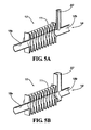
FIG. 5A depicts a perspective longitudinal cross-section view of a twisted waveguide structure with a coaxial power coupling according to an embodiment of the invention;
FIG. 5B depicts a perspective longitudinal cross-section view of a twisted waveguide structure with a rectangular waveguide power coupling according to an embodiment of the invention;
FIG. 6A depicts a perspective view of a non-twisted waveguide connected at each end of a twisted waveguide structure according to an embodiment of the invention;
FIG. 6B depicts a perspective longitudinal cross-section view, taken along line D-D, of a non-twisted waveguide connected at each end of a twisted waveguide structure according to an embodiment of the invention;
FIG. 6C depicts a perspective longitudinal cross-section view of a non-twisted waveguide connected at each end of a twisted waveguide structure according to an embodiment of the invention;
FIGS. 7A and 7B depict partial transverse views of symmetrically twisted waveguide structures according to an embodiment of the invention;
FIG. 7C depicts a partial longitudinal cross-section view of a symmetrically twisted waveguide structure according to an embodiment of the invention;
FIGS. 8A and 8B depict partial transverse views of asymmetrically twisted waveguide structures according to an embodiment of the invention;
FIG. 8C depicts a partial longitudinal cross-section view of an asymmetrically twisted waveguide structure according to an embodiment of the invention;
FIG. 9 depicts a perspective view of a twisted waveguide structure having a rectangular transverse cross-section according to an embodiment of the invention; and
FIG. 10 depicts predicted dispersion curves for twisted waveguide structures having various twist rates compared to the free-space propagation.
DETAILED DESCRIPTION OF THE INVENTION
FIGS. 1A, 1B and 1C depict various views of a first embodiment of a twisted waveguide structure 10. In this embodiment, a waveguide body 11 defines two opposing helical channels 12 a-12 b (FIGS. 1A, 1B) which merge along the central axis of the structure to form a central axial channel 16. As shown in the cross-section view of FIG. 1B, the channels 12 a-12 b are nearly elliptically shaped in a direction transverse to the central axis. The channels 12 a-12 b are separated by opposing lobe structures 14 a-14 b. As shown in FIG. 1C, the structure 10 forms a corrugated pattern of grooves and ridges in the longitudinal cross-section. The pitch of this corrugated pattern may be characterized by a pitch angle θ as shown in FIG. 1C or by a pitch rate expressed in revolutions per meter (R/m) for example.
Although the invention is not limited to any particular theory of operation, it has been determined that a twisting waveguide, such as the helical structures described herein, effectively increases the path length of propagation of the electromagnetic wave energy traveling through the structure. Increased volume of the space occupied by the electromagnetic wave energy also results in increased propagation delay. The central axial channel 16 remains open as a circular aperture along the longitudinal axis through which the particle beam may pass. The speed of the electromagnetic wave propagation is determined at least in part by the cross sectional shape and twist rate (pitch) of the structure.
FIG. 10 depicts predicted dispersion curves for a twisted waveguide structure. These results, which are plotted in a frequency (in GHZ)-versus-phase, β (in R/m) diagram (β=2π/λ, where λ is the free-space wavelength), are calculated using computer simulations which apply a two-dimensional frequency domain method. The straight line 24 represents a limit at which the speed of the transverse electromagnetic (TEM) wave propagation equals the speed of light in free space. The curves crossing the TEM limit 24 represent various pitch rates, p, expressed in revolutions per meter (R/m) ranging from 67.3 R/m to 337 R/m, where the wave propagation is faster than the speed of light on the left side of the TEM limit 24 (with slow twist) and slower than the speed of light on the right side of the TEM limit 24 (with faster twist). The curve for a straight waveguide 25 stays on the left side of the line 24. The simulation results indicate how the pitch of the waveguide twist affects the speed of wave propagation in the twisted guide.
Generally, the lowest order Transverse Magnetic (TM) mode is the most efficient mode for particle acceleration. Actually, the TM-modes in a twisted waveguide structure are more accurately described as “TM-like-modes” as they are not true TM-modes in the conventional mathematical coordinate system. The longitudinal component of the electric field of the TM-like-mode wave in the central axial channel 16 is very similar to that of a true TM-mode wave, and this TM-like-mode wave can accelerate particles at a velocity that is matched to the wave propagation. Although an infinite number of modes exist in any accelerating structure, the specific accelerating mode electric field is almost the strongest near the center of the structure. The larger triangles near the center of the axial channel 16 in the field strength representations in FIGS. 1C and 2B show this. Generally, the quality factor, Q, of the structure determines the strength of the accelerating field. Computer simulations and laboratory measurements have confirmed that the accelerating field strength in a twisted waveguide is comparable to the field strength in a conventional structure.
Since the resonant RF frequency of the structure 10 is determined by characteristics of the overall structure (i.e., channel dimensions and pitch), the resonant frequency can be tuned with a tuning mechanism that can change the volume by slightly moving the wall at the end of the structure. It is also possible to use a tuning/phase-shifting device disposed external to the structure 10 and in communication with an inlet/outlet. For example, as shown in FIGS. 6A, 6B, and 6C, a rectangular waveguide 22 can be integrated with the structure 10. An RF phase-shifter can be disposed in the waveguide 22 to adjust the overall resonant frequency of the structure 10. Power couplers and higher-order mode (HOM) dampers 23 (FIG. 6C) can also be disposed in the waveguide 22. The embodiments of FIGS. 6A-6C include straight circular waveguide sections 18 a-18 b at each end of the waveguide body 11. The embodiment of FIG. 6C includes an additional waveguide connection 26 at the bottom of the straight waveguide section 22.
FIGS. 5A and 5B depict an embodiment of a twisted waveguide structure 10 incorporating a power coupler 20 which may be either a coaxial type (FIG. 5A) or rectangular type (FIG. 5B) directly connected transverse to the central axis of the waveguide body 11.
Twisted waveguide structures generally fall into two categories: symmetrically twisted structures and asymmetrically twisted structures. As shown in FIGS. 7A-7C, waveguides having an even number of lobe structures, such as two lobe structures 14 a-14 b (FIG. 7A) or four lobe structures 14 a, 14 b, 14 c, 14 d (FIG. 7B), have a vertically symmetrical longitudinal cross section (FIG. 7C). As shown in FIGS. 8A-8C, waveguides having an odd number of lobe structures, such as one lobe structure 14 a (FIG. 8A) or three lobe structures 14 a-14 c (FIG. 8B), have a vertically asymmetrical longitudinal cross section (as shown in FIG. 8C).
FIGS. 2A, 2B, 3, 4A and 4B depict various views of a second embodiment of a twisted waveguide structure 10. In this embodiment, the waveguide body 11 (FIGS. 2A, 2B, 3, 4A) also includes two opposing helical channels 12 a (FIGS. 2A, 3, 4A, 4B) and 12 b (FIGS. 2A, 3, 4A) which merge along the axis of the structure to form a central axial channel 16. As shown in the transverse cross-section view of FIG. 4A (viewed at section line E-E in FIG. 3), the channels 12 a-12 b are shaped as sections of a circle which are separated by opposing lobe structures 14 a-14 b. As shown in FIG. 2B, the structure 10 forms a corrugated pattern of grooves and ridges in the longitudinal cross-section, the longitudinal pitch of which may be characterized by the pitch angle θ.
In comparing the first embodiment (FIGS. 1A-1C) to the second embodiment (FIGS. 2A-2B, 3 and 4A-4B), the first embodiment may provide better particle beam quality, whereas the second may provide higher electrical efficiency.
FIG. 9 depicts an alternative embodiment of a twisted waveguide structure 10 wherein the waveguide body 10 comprises a single channel having a rectangular transverse cross-section.
The twisted waveguide structures described herein are particularly suited to formation by extrusion molding. However, these structures could also be formed by injection molding or casting for example. Materials such as ferrous and nonferrous metals and their alloys, or reinforced plastics, composites and the like with metal plated inner surface may be used to form the waveguide body 11. Thus, production costs, fabrication times, and fine tuning of these structures are significantly less than doing the same with the corrugated structures manufactured by welding or brazing individual components.
The foregoing description of preferred embodiments for this invention have been presented for purposes of illustration and description. They are not intended to be exhaustive or to limit the invention to the precise form disclosed. Obvious modifications or variations are possible in light of the above teachings. The embodiments are chosen and described in an effort to provide the best illustrations of the principles of the invention and its practical application, and to thereby enable one of ordinary skill in the art to utilize the invention in various embodiments and with various modifications as are suited to the particular use contemplated. All such modifications and variations are within the scope of the invention as determined by the appended claims when interpreted in accordance with the breadth to which they are fairly, legally, and equitably entitled.

Claims (12)

1. An electromagnetic waveguide structure comprising:
a waveguide body having a central axis;
at least two helical channels defined by the waveguide body, the channels twisted about one another and about the central axis, each helical channel operable to support electromagnetic wave propagation in at least one propagation mode at a propagation speed determined by a pitch rate of the at least two helical channels, wherein the pitch rate is expressed in revolutions of the helical channels per unit length along the central axis; and
a substantially linear central axial channel through the waveguide body, disposed along the central axis and operable to conduct a charged particle beam,
wherein portions of the at least two helical channels disposed nearest to the central axis merge with the linear central axial channel, such that the portions of the helical channels disposed nearest to the central axis are open to the linear central axial channel.
2. The electromagnetic waveguide structure of claim 1 wherein the at least two helical channels comprise more than two helical channels disposed at a substantially equiangular spacing around the central axis in a plane transverse to the central axis.
3. The electromagnetic waveguide structure of claim 1 wherein the at least two helical channels comprise two helical channels disposed on opposing sides of the central axis, each helical channel having a substantially elliptically-shaped cross-section in a plane transverse to the central axis.
4. The electromagnetic waveguide structure of claim 1 wherein the at least two helical channels comprise two helical channels disposed on opposing sides of the central axis, each helical channel having a cross-section shaped as a portion of a circle in a plane transverse to the central axis.
5. The electromagnetic waveguide structure of claim 1 further comprising a rectangular waveguide section coupled to the central axial channel at opposing ends thereof.
6. The electromagnetic waveguide structure of claim 1 formed by a process selected from the group consisting of extrusion molding, injection molding and casting.
7. The electromagnetic waveguide structure of claim 1 further comprising at least one straight waveguide section aligned coaxially with the central axis and coupled to at least one end of the central axial channel and operable to conduct the charged particle beam.
8. The electromagnetic waveguide structure of claim 7 further comprising a power coupler connected to the at least one straight waveguide section and aligned substantially perpendicular to the central axis.
9. An electromagnetic waveguide structure comprising:
a waveguide body having a central axis;
a substantially linear central axial channel disposed through the waveguide body along the central axis and operable to conduct a charged particle beam,
a first helical channel defined by the waveguide body and disposed about the central axial channel, the first helical channel operable to support electromagnetic wave propagation in a transverse magnetic propagation mode, wherein a central portion of the first helical channel disposed nearest to the central axis is open to the linear central axial channel; and
a second helical channel defined by the waveguide body and disposed about the central axial channel radially opposite the first helical channel, whereby the second helical channel intertwines with the first helical channel such that the first and second helical channels are twisted about one another, the second helical channel operable to support electromagnetic wave propagation in the transverse magnetic propagation mode, wherein a central portion of the second helical channel disposed nearest to the central axis is open to the linear central axial channel.
10. The electromagnetic waveguide structure of claim 9 wherein the first and second helical channels each have a substantially elliptically-shaped cross-section in a plane transverse to the central axis.
11. The electromagnetic waveguide structure of claim 9 wherein the first and second helical channels each have a cross-section shaped as a section of a circle in a plane transverse to the central axis.
12. The electromagnetic waveguide structure of claim 9 formed by a process selected from the group consisting of extrusion molding, injection molding and casting.
US12/784,571 2010-05-21 2010-05-21 Slow wave structures using twisted waveguides for charged particle applications Active 2031-07-30 US8330372B2 (en)

Priority Applications (1)

Application Number Priority Date Filing Date Title
US12/784,571 US8330372B2 (en) 2010-05-21 2010-05-21 Slow wave structures using twisted waveguides for charged particle applications

Applications Claiming Priority (1)

Application Number Priority Date Filing Date Title
US12/784,571 US8330372B2 (en) 2010-05-21 2010-05-21 Slow wave structures using twisted waveguides for charged particle applications

Publications (2)

Publication Number Publication Date
US20110285479A1 US20110285479A1 (en) 2011-11-24
US8330372B2 true US8330372B2 (en) 2012-12-11

Family

ID=44972028

Family Applications (1)

Application Number Title Priority Date Filing Date
US12/784,571 Active 2031-07-30 US8330372B2 (en) 2010-05-21 2010-05-21 Slow wave structures using twisted waveguides for charged particle applications

Country Status (1)

Country Link
US (1) US8330372B2 (en)

Cited By (4)

* Cited by examiner, † Cited by third party
Publication number Priority date Publication date Assignee Title
CN106257745A (en) * 2016-08-29 2016-12-28 成都赛纳为特科技有限公司 A kind of twisted waveguide combination type tiltedly turns round coupling rectangular folded waveguide
CN108682607A (en) * 2018-05-03 2018-10-19 电子科技大学 A kind of U-shaped micro-strip slow-wave structure of corrugated casing
US11202362B1 (en) * 2018-02-15 2021-12-14 Christopher Mark Rey Superconducting resonant frequency cavities, related components, and fabrication methods thereof
US11211676B2 (en) * 2019-10-09 2021-12-28 Com Dev Ltd. Multi-resonator filters

Families Citing this family (13)

* Cited by examiner, † Cited by third party
Publication number Priority date Publication date Assignee Title
CN106159402A (en) * 2016-08-29 2016-11-23 成都赛纳为特科技有限公司 A kind of twisted waveguide combination type tiltedly turns round the single ridge rectangle folded waveguide of coupling
CN106252811A (en) * 2016-08-29 2016-12-21 成都赛纳为特科技有限公司 A kind of twisted waveguide combination type tiltedly turns round coupling folded waveguide
CN106207358A (en) * 2016-08-29 2016-12-07 成都赛纳为特科技有限公司 A kind of twisted waveguide separate type tiltedly turns round the single ridge rectangle folded waveguide of coupling
CN106207357A (en) * 2016-08-29 2016-12-07 成都赛纳为特科技有限公司 A kind of twisted waveguide separate type directrix plane ridge waveguide folded waveguide
CN106252812A (en) * 2016-08-29 2016-12-21 成都赛纳为特科技有限公司 A kind of twisted waveguide separate type tiltedly turns round coupling folded waveguide
CN106159403A (en) * 2016-08-29 2016-11-23 成都赛纳为特科技有限公司 A kind of twisted waveguide combination type tiltedly turns round the double ridge rectangle folded waveguide of coupling
CN106207356A (en) * 2016-08-29 2016-12-07 成都赛纳为特科技有限公司 A kind of twisted waveguide separate type tiltedly turns round the double ridge rectangle folded waveguide of coupling
CN106252809A (en) * 2016-08-29 2016-12-21 成都赛纳为特科技有限公司 A kind of twisted waveguide separate type tiltedly turns round coupling rectangular folded waveguide
CN106329050A (en) * 2016-08-29 2017-01-11 成都赛纳为特科技有限公司 Twisted waveguide-combined quasi-plane folded waveguide
CN106159400A (en) * 2016-08-29 2016-11-23 成都赛纳为特科技有限公司 A kind of twisted waveguide separate type directrix plane folded waveguide
CN111029709B (en) * 2019-12-30 2021-05-28 南京驰韵科技发展有限公司 Preparation process of 90-degree ultrathin rotary twisted waveguide
GB202006503D0 (en) * 2020-05-01 2020-06-17 Elekta ltd Waveguide for a liner accelerator
CN114530358B (en) * 2022-02-22 2023-04-18 电子科技大学 Coaxial single-electron-beam multi-channel helix traveling wave tube

Citations (3)

* Cited by examiner, † Cited by third party
Publication number Priority date Publication date Assignee Title
US2541843A (en) * 1947-07-18 1951-02-13 Philco Corp Electronic tube of the traveling wave type
US4710736A (en) * 1983-07-05 1987-12-01 Stidwell Alan G Flexible waveguides with 45° corrugations to allow bending and twisting of waveguides
US7190860B2 (en) 2005-04-26 2007-03-13 Harris Corporation Spiral waveguide slow wave resonator structure

Patent Citations (3)

* Cited by examiner, † Cited by third party
Publication number Priority date Publication date Assignee Title
US2541843A (en) * 1947-07-18 1951-02-13 Philco Corp Electronic tube of the traveling wave type
US4710736A (en) * 1983-07-05 1987-12-01 Stidwell Alan G Flexible waveguides with 45° corrugations to allow bending and twisting of waveguides
US7190860B2 (en) 2005-04-26 2007-03-13 Harris Corporation Spiral waveguide slow wave resonator structure

Non-Patent Citations (1)

* Cited by examiner, † Cited by third party
Title
Zhong Shi-Cai, Microwave Tuning of Disk-Loaded Waveguide for BEPC, 1987, 802-803, IEEE, Institute of High Energy Physics, Beijing, PRC.

Cited By (4)

* Cited by examiner, † Cited by third party
Publication number Priority date Publication date Assignee Title
CN106257745A (en) * 2016-08-29 2016-12-28 成都赛纳为特科技有限公司 A kind of twisted waveguide combination type tiltedly turns round coupling rectangular folded waveguide
US11202362B1 (en) * 2018-02-15 2021-12-14 Christopher Mark Rey Superconducting resonant frequency cavities, related components, and fabrication methods thereof
CN108682607A (en) * 2018-05-03 2018-10-19 电子科技大学 A kind of U-shaped micro-strip slow-wave structure of corrugated casing
US11211676B2 (en) * 2019-10-09 2021-12-28 Com Dev Ltd. Multi-resonator filters

Also Published As

Publication number Publication date
US20110285479A1 (en) 2011-11-24

Similar Documents

Publication Publication Date Title
US8330372B2 (en) Slow wave structures using twisted waveguides for charged particle applications
KR101983333B1 (en) Vacuum electron device drift tube
US20080068112A1 (en) Rod-loaded radiofrequency cavities and couplers
US9786464B2 (en) Superconducting multi-cell trapped mode deflecting cavity
Jensen RF cavity design
US8941446B2 (en) Ferrite circulator with integrated E-plane transition
US8232749B1 (en) Dual slot resonance coupling for accelerators
EP1158594B1 (en) Generator of circularly polarized wave
CN102339708B (en) Gradient ridge loading tortuous waveguide slow wave line
CN107196022B (en) Edge hole disc-loaded waveguide multi-frequency controllable mode converter
JP5071859B2 (en) Right / left-handed composite waveguide and manufacturing method thereof
US20140266948A1 (en) Compact corrugated feedhorn
Simakov et al. Optimizing the configuration of a superconducting photonic band gap accelerator cavity to increase the maximum achievable gradients
Yang et al. Electromagnetic analysis on propagation characteristics of CRLH waveguide loaded with double ridge corrugations
Guan et al. Design of a 220-GHz continuous frequency-tunable gyrotron with quasi-optical cavity
Kang Twisted waveguide accelerating structure
CN114566773B (en) Circular waveguide TM01-TE01 mode converter loaded by spiral grating groove
Wang et al. Elliptical Cavity Shape Optimization for Acceleration and HOM Damping
Chipengo et al. Dispersion Engineering for Slow‐Wave Structure Design
Juntong et al. Optimisation of the new low surface field accelerating structure for the ILC
JP2010273151A (en) Mode converter, power synthesizer/distributor and plane magic t
Abdoli-Arani et al. Dispersion relation and electron acceleration in the combined circular and elliptical metallic-dielectric waveguide filled by plasma
Fan et al. Simulations for the advanced photonic band gap accelerating structure
Serpico THE FERMI FREE ELECTRON LASER: A HIGH GRADIENT SOLUTION FOR INCREASING THE LINEAR ACCELERATOR ENERGY
Smirnova Novel Photonic Band Gap structures for accelerator applications

Legal Events

Date Code Title Description
AS Assignment

Owner name: UT-BATTELLE, LLC, TENNESSEE

Free format text: ASSIGNMENT OF ASSIGNORS INTEREST;ASSIGNOR:KANG, YOON W.;REEL/FRAME:024671/0821

Effective date: 20100629

Owner name: UNIVERSITY OF TENNESSEE RESEARCH FOUNDATION, TENNE

Free format text: ASSIGNMENT OF ASSIGNORS INTEREST;ASSIGNORS:FATHY, ALY E.;WILSON, JOSHUA L.;SIGNING DATES FROM 20100601 TO 20100702;REEL/FRAME:024671/0794

AS Assignment

Owner name: U.S. DEPARTMENT OF ENERGY, DISTRICT OF COLUMBIA

Free format text: CONFIRMATORY LICENSE;ASSIGNOR:BATTELLE MEMORIAL INSTITUTE, PACIFIC NORTHWEST DIVISION;REEL/FRAME:024832/0508

Effective date: 20100625

STCF Information on status: patent grant

Free format text: PATENTED CASE

FPAY Fee payment

Year of fee payment: 4

MAFP Maintenance fee payment

Free format text: PAYMENT OF MAINTENANCE FEE, 8TH YR, SMALL ENTITY (ORIGINAL EVENT CODE: M2552); ENTITY STATUS OF PATENT OWNER: SMALL ENTITY

Year of fee payment: 8