US8324812B2 - Protecting ballast circuitry against miswiring - Google Patents
Protecting ballast circuitry against miswiring Download PDFInfo
- Publication number
- US8324812B2 US8324812B2 US12/409,616 US40961609A US8324812B2 US 8324812 B2 US8324812 B2 US 8324812B2 US 40961609 A US40961609 A US 40961609A US 8324812 B2 US8324812 B2 US 8324812B2
- Authority
- US
- United States
- Prior art keywords
- voltage
- circuit
- controller
- depletion mode
- mode mosfet
- Prior art date
- Legal status (The legal status is an assumption and is not a legal conclusion. Google has not performed a legal analysis and makes no representation as to the accuracy of the status listed.)
- Expired - Fee Related, expires
Links
Images


Classifications
-
- H—ELECTRICITY
- H05—ELECTRIC TECHNIQUES NOT OTHERWISE PROVIDED FOR
- H05B—ELECTRIC HEATING; ELECTRIC LIGHT SOURCES NOT OTHERWISE PROVIDED FOR; CIRCUIT ARRANGEMENTS FOR ELECTRIC LIGHT SOURCES, IN GENERAL
- H05B41/00—Circuit arrangements or apparatus for igniting or operating discharge lamps
- H05B41/14—Circuit arrangements
- H05B41/26—Circuit arrangements in which the lamp is fed by power derived from dc by means of a converter, e.g. by high-voltage dc
- H05B41/28—Circuit arrangements in which the lamp is fed by power derived from dc by means of a converter, e.g. by high-voltage dc using static converters
- H05B41/282—Circuit arrangements in which the lamp is fed by power derived from dc by means of a converter, e.g. by high-voltage dc using static converters with semiconductor devices
- H05B41/285—Arrangements for protecting lamps or circuits against abnormal operating conditions
- H05B41/2851—Arrangements for protecting lamps or circuits against abnormal operating conditions for protecting the circuit against abnormal operating conditions
- H05B41/2853—Arrangements for protecting lamps or circuits against abnormal operating conditions for protecting the circuit against abnormal operating conditions against abnormal power supply conditions
-
- Y—GENERAL TAGGING OF NEW TECHNOLOGICAL DEVELOPMENTS; GENERAL TAGGING OF CROSS-SECTIONAL TECHNOLOGIES SPANNING OVER SEVERAL SECTIONS OF THE IPC; TECHNICAL SUBJECTS COVERED BY FORMER USPC CROSS-REFERENCE ART COLLECTIONS [XRACs] AND DIGESTS
- Y02—TECHNOLOGIES OR APPLICATIONS FOR MITIGATION OR ADAPTATION AGAINST CLIMATE CHANGE
- Y02B—CLIMATE CHANGE MITIGATION TECHNOLOGIES RELATED TO BUILDINGS, e.g. HOUSING, HOUSE APPLIANCES OR RELATED END-USER APPLICATIONS
- Y02B20/00—Energy efficient lighting technologies, e.g. halogen lamps or gas discharge lamps
Definitions
- the present disclosure relates to circuitry for use with the ignition of gas discharge lamps and particularly to circuitry employing an electronic ballast with circuitry for interfacing with ballast with a remote controller operative for effecting dimming of the gas discharge lamps.
- a remote controller operative for effecting dimming of the gas discharge lamps.
- the present disclosure provides a solution to the above described problem by employing depletion mode MOSFETS in both sides of the circuit for connection to the remote controller for the gas discharge lamps in a manner that utilizes the switching properties of the depletion mode MOSFETS to respond to an overvoltage, including reversal of polarity, to create an open circuit condition in the circuit to the remote controller.
- FIG. 1 is a schematic of the circuitry of the present disclosure
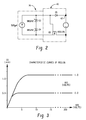
- FIG. 2 is an alternate arrangement of the interface circuitry portion of FIG. 1 ;
- FIG. 3 is a graph of the characteristic curves of the depletion mode MOSFETS of the type employed in the present disclosure.
- an electronic ballast circuit for gas discharge lamps is indicated generally in dashed outline by reference numeral 10 and may be of a conventional or well known design operative for connection at terminals 12 , 14 to opposite sides of a power line indicated generally at LV.
- the ballast circuitry 10 is connected to an interface circuit indicated generally by reference numeral 16 which receives relatively low voltage D.C.
- the interface circuit 16 connects with the electronic ballast internally at junctions 20 , 22 .
- the interface circuit 16 provides a relatively low current signal of about 500 microamp along lines 24 , 26 to the input of a protection circuit indicated generally at 30 .
- the circuit 30 transfers the 500 microamp current signal at output terminals 32 , 34 which may be connected to respectively the positive and negative terminals of a low voltage controller indicated by dashed-dot line and reference numeral 38 .
- the controller 38 is of the type which provides a variable impedance or resistance in response to a sensed condition such as, for example, the movement of a control element or member by the user, or by the signal from a sensor such as a motion, photoelectric, infrared, Doppler or other condition responsive sensor.
- the change in impedance (unshown) of the controller provides a variable or bi-level voltage signal for changing the voltage of the interface circuit for controlling dimming of the output of the electronic ballast to the gas discharge lamps.
- the positive lead 24 of the interface circuit is connected to the source of switching device Q 3 ; and, the drain is connected to the connector terminal 32 for connection to controller 38 .
- the gate of Q 3 is connected to the opposite side 26 of the signal line.
- the device Q 3 has an intrinsic diode D 5 connected between the source and drain such that the device conducts so long as the voltage applied to the positive terminal in connector 32 is not greater than the 12 volt supply by virtue of the blocking diode D 5 .
- the upper transistor Q 3 In the event a negative voltage greater than negative 12 is applied to the terminals, the upper transistor Q 3 will continue to conduct; and, if the gate to source voltage is greater than its threshold voltage which is typically around ⁇ 2.5 Volts, the device will be in its ON state and the current source will supply 500 microamps to the controller. As the negative voltage increases in magnitude, i.e. gets more negative, current will continue to flow at the same level, but the drain to source voltage of the lower transistor Q 4 will increase; and, the device Q 4 matches the amplitude of the current source at the higher voltages to until the avalanche voltage of the device is reached, which in the present practice is about 600 volts.
- the circuit 30 of the arrangement of FIG. 1 protects the interface circuit 16 from overvoltage, either positive or negative, in the event of miswiring a connection of terminals 32 , 34 to a power line.
- the electronic ballast circuit 10 , the interface circuit 16 and the protection circuitry 30 may be incorporated into a common housing with a pair of color coded leads extending to terminals 12 , 14 for a connection to a power line and with another pair of differently color coded leads extending therefrom for connection to terminals 32 , 34 for connection to a remote controller.
- an alternative arrangement of the interface circuit is indicated generally at 40 and has about 500 microamps of current supplied from the interface circuit 16 with diodes D 3 , D 4 connected across the line thereof.
- Protection circuitry 40 of the arrangement of FIG. 2 has a switching device Q 5 connected in the negative side of the 12 volt signal line similar to the switching device Q 4 of FIG. 1 , which device Q 5 may also be of the depletion mode MOSFET type.
- the positive side of the line 42 has a diode D 5 connected therein; and, upon miswiring and application of a high voltage to the terminal 42 , the diode continues to conduct current flow in the line.
- the voltage on switching device Q 5 continues to increase until an avalanche condition occurs as in paragraph.
- the drain to source voltage of the device Q 5 will be able to increase with the external voltage and prevent the device Q 5 from switching to open circuit. If the polarity of the external source is reversed, D 5 will block if this voltage exceeds about 12 Volts. The difference is that the version of FIG. 1 will not have a diode drop because the channel of Q 3 will continue to conduct until the threshold voltage is reached. In this way, the version of FIG. 1 has better linearity, especially at low controller voltages, i.e. voltages below 2.5 Volts.
- FIG. 3 typical characteristics of the type BSS 126 switching devices employed are shown where it is noted that the current is maintained, substantially constant so long as the gate voltage is maintained irrespective of the source to drain voltage.
- the present circuitry provides unique low cost and simple additions to an electronic ballast and interface circuitry for gas discharge lamps where it is desired to connect a controller for dimming the lamps to the circuitry and to provide protection in the event the ballast is miswired to the power line.
Landscapes
- Circuit Arrangements For Discharge Lamps (AREA)
Abstract
A circuit for protecting an electronic ballast for use with a remote controller for gas discharge lamps against miswiring to a power source. Depletion mode MOSFETS are employed in both sides of the circuit to the controller and the MOSFETS respond to overvoltage, including polarity reversal to create an open circuit condition in the circuit to the controller.
Description
The present disclosure relates to circuitry for use with the ignition of gas discharge lamps and particularly to circuitry employing an electronic ballast with circuitry for interfacing with ballast with a remote controller operative for effecting dimming of the gas discharge lamps. Presently, it is common practice to house the ballast circuitry and interface circuitry in a common housing with a set of electrical leads extending therefrom for connection to a power line such as a 120 volt/240 volt single phase AC line and another set of electrical leads for outputting a low voltage low operage signal to the dimming controller.
In service, there has been encountered instances where, despite appropriate color coding of each set of electrical leads, the low voltage signal leads intended for connection to the controller have been miswired and connected to a line voltage power source. The connection of the low voltage interface circuit leads to the line power has resulted in an over current condition and burn out of the electronic ballast circuitry.
Heretofore, attempts to protect the ballast interface circuitry and ballast against over voltage have utilized a positive temperature coefficient or PTC thermistor which responds to the higher voltage by heating and increasing the resistance thereby reducing the current flow in the interface circuit. The PTC is operable to return to its lower or cold resistance state when the overvoltage is removed thereby enabling resumption of the low voltage operation with the remote controller. However, where the circuitry is encased in a potting compound, it is necessary to isolate the PTC from the potting compound to protect the potting compound from the elevated temperatures generated by the PTC in the event of miswiring. This has resulted in added cost due to the necessity of rearranging the circuitry to isolate the PTC.
Thus, it has been desired to find a simple and relatively low cost technique for protecting the controller interface circuitry employed with an electronic ballast for a gas discharge lamp from miswiring by connecting the low voltage controller leads to a high voltage power line.
The present disclosure provides a solution to the above described problem by employing depletion mode MOSFETS in both sides of the circuit for connection to the remote controller for the gas discharge lamps in a manner that utilizes the switching properties of the depletion mode MOSFETS to respond to an overvoltage, including reversal of polarity, to create an open circuit condition in the circuit to the remote controller.
In the event of miswiring the leads for the low voltage controller to the high voltage power line, upon the voltage exceeding the voltage range of the controller in the positive direction one MOSFET goes open circuit; and, upon the voltage decreasing negatively outside a low voltage threshold, the MOSFET on the opposite side of the line switches to an open circuit condition thereby protecting the interface circuitry against mis-connection to a live voltage a.c. power.
Referring to FIG. 1 , an electronic ballast circuit for gas discharge lamps is indicated generally in dashed outline by reference numeral 10 and may be of a conventional or well known design operative for connection at terminals 12, 14 to opposite sides of a power line indicated generally at LV. The ballast circuitry 10 is connected to an interface circuit indicated generally by reference numeral 16 which receives relatively low voltage D.C. power denoted, as for example 15 volts, from the electronic ballast and which is converted to a current level of about 500 microamps (500 μA) by transistor Q1 which may be of the MOSFET variety and current limiting resistor R1 which has a value of nominally 5 kilo ohms Zener diodes D1, D2, which may be 1N5242 devices, limit the voltage between lines 24 and 26 to about 12 Volts. The interface circuit 16 connects with the electronic ballast internally at junctions 20, 22.
The interface circuit 16 provides a relatively low current signal of about 500 microamp along lines 24, 26 to the input of a protection circuit indicated generally at 30. The circuit 30 transfers the 500 microamp current signal at output terminals 32, 34 which may be connected to respectively the positive and negative terminals of a low voltage controller indicated by dashed-dot line and reference numeral 38.
Typically, the controller 38 is of the type which provides a variable impedance or resistance in response to a sensed condition such as, for example, the movement of a control element or member by the user, or by the signal from a sensor such as a motion, photoelectric, infrared, Doppler or other condition responsive sensor. The change in impedance (unshown) of the controller provides a variable or bi-level voltage signal for changing the voltage of the interface circuit for controlling dimming of the output of the electronic ballast to the gas discharge lamps.
The positive lead 24 of the interface circuit is connected to the source of switching device Q3; and, the drain is connected to the connector terminal 32 for connection to controller 38. The gate of Q3 is connected to the opposite side 26 of the signal line. Referring to the enlarged view in FIG. 1 , the device Q3 has an intrinsic diode D5 connected between the source and drain such that the device conducts so long as the voltage applied to the positive terminal in connector 32 is not greater than the 12 volt supply by virtue of the blocking diode D5. In the event a negative voltage greater than negative 12 is applied to the terminals, the upper transistor Q3 will continue to conduct; and, if the gate to source voltage is greater than its threshold voltage which is typically around −2.5 Volts, the device will be in its ON state and the current source will supply 500 microamps to the controller. As the negative voltage increases in magnitude, i.e. gets more negative, current will continue to flow at the same level, but the drain to source voltage of the lower transistor Q4 will increase; and, the device Q4 matches the amplitude of the current source at the higher voltages to until the avalanche voltage of the device is reached, which in the present practice is about 600 volts. Thus, the circuit 30 of the arrangement of FIG. 1 protects the interface circuit 16 from overvoltage, either positive or negative, in the event of miswiring a connection of terminals 32, 34 to a power line.
In the present practice, the electronic ballast circuit 10, the interface circuit 16 and the protection circuitry 30 may be incorporated into a common housing with a pair of color coded leads extending to terminals 12, 14 for a connection to a power line and with another pair of differently color coded leads extending therefrom for connection to terminals 32, 34 for connection to a remote controller.
Referring to FIG. 2 , an alternative arrangement of the interface circuit is indicated generally at 40 and has about 500 microamps of current supplied from the interface circuit 16 with diodes D3, D4 connected across the line thereof. Protection circuitry 40 of the arrangement of FIG. 2 has a switching device Q5 connected in the negative side of the 12 volt signal line similar to the switching device Q4 of FIG. 1 , which device Q5 may also be of the depletion mode MOSFET type. In the arrangement of FIG. 2 the positive side of the line 42 has a diode D5 connected therein; and, upon miswiring and application of a high voltage to the terminal 42, the diode continues to conduct current flow in the line. The voltage on switching device Q5 continues to increase until an avalanche condition occurs as in paragraph.
The drain to source voltage of the device Q5 will be able to increase with the external voltage and prevent the device Q5 from switching to open circuit. If the polarity of the external source is reversed, D5 will block if this voltage exceeds about 12 Volts. The difference is that the version of FIG. 1 will not have a diode drop because the channel of Q3 will continue to conduct until the threshold voltage is reached. In this way, the version of FIG. 1 has better linearity, especially at low controller voltages, i.e. voltages below 2.5 Volts.
Referring to FIG. 3 , typical characteristics of the type BSS 126 switching devices employed are shown where it is noted that the current is maintained, substantially constant so long as the gate voltage is maintained irrespective of the source to drain voltage.
The present circuitry provides unique low cost and simple additions to an electronic ballast and interface circuitry for gas discharge lamps where it is desired to connect a controller for dimming the lamps to the circuitry and to provide protection in the event the ballast is miswired to the power line.
The invention has been described with reference to the preferred embodiments. Obviously, modifications and alterations will occur to others upon reading and understanding the preceding detailed description. It is intended that the invention be construed as including all such modifications and alterations.
Claims (14)
1. A method of protecting an electronic ballast for a gas discharge lamp comprising:
(a) connecting a voltage interface circuit intermediate a control circuit and the electronic ballast;
(b) disposing a protection circuit including first and second circuit branches extending between the voltage interface circuit and the controller connection with a voltage responsive depletion mode MOSFET switch in circuit with the first branch and a diode in circuit in the second branch; and,
(c) automatically opening said voltage responsive depletion mode MOSFET switch when one of (i) an overvoltage condition occurs and (ii) the controller connection is connected to a reverse polarity power source, and when a power source voltage at the controller connection is one of (i) less than −2 volts and (ii) greater than +10 volts.
2. The method defined in claim 1 , wherein disposing a voltage responsive switch includes disposing the depletion mode MOSFET switch with the source and drain series connected in the first branch.
3. The method defined in claim 2 , wherein disposing a depletion mode MOSFET switch includes connecting a gate junction thereof to the second branch of the protection circuit.
4. The method defined in claim 1 , wherein connecting the voltage interface circuit and the controller to the circuit includes connecting circuitry requiring about 500 μ amperes current flow.
5. The circuit defined in claim 1 , wherein the depletion mode MOSFET switch is operative to open automatically when the voltage is one of (i) less than −2 volts and (ii) greater than +12 volts.
6. A circuit for protecting an electronic ballast with controller for use with a gas discharge lamp comprising:
(a) a voltage interface circuit powered by the electronic ballast and connected intermediate the electronic ballast and a controller; and,
(b) a protection circuit including first and second circuit branches extending between the voltage interface circuit and the controller connection with a series depletion MOSFET switch disposed in the first branch and a diode in the second branch of the line between the voltage interface circuit and the controller, wherein the depletion MOSFET switch is operative to open automatically upon the occurrence of one of (i) an overvoltage at the controller connection and (ii) a reverse polarity connection to the controller connection, and when a power source voltage at the controller connection is one of (i) less than −2 volts and (ii) greater than +10 volts.
7. The circuit defined in claim 6 , wherein series depletion MOSFET switch includes a diode.
8. The circuit defined in claim 6 , wherein the depletion mode MOSFET switch is operable according to the following
where Vc is the voltage applied to the controller connection, D5 is the diode and Q5 is the depletion mode MOSFET switch.
9. The circuit defined in claim 6 , wherein the depletion mode MOSFET switch is operable according to the following
where Vc is the voltage applied to the controller connection, Q3+D5 is one of the depletion mode MOSFET switching devices with an intrinsic diode D5 shunting the source and drain terminals thereof and connected in a positive branch of the controller, Q4 is another of the depletion mode MOSFET switching devices connected in a negative branch of the controller connection.
10. A circuit for protecting an electronic controllable ballast for use with a gas discharge lamp comprising:
(a) a ballast interface circuit receiving power from the ballast and providing a relatively low voltage output for connection to a voltage controller;
(b) a protection circuit including first and second circuit branches extending between the ballast interface circuit and the voltage controller connection with at least one voltage responsive depletion mode MOSFET switching device disposed in one of the first and second branches and a diode in the other of the first and second branch between the ballast interface circuit and the voltage controller, wherein the voltage responsive depletion mode MOSFET switching device is operable to switch to an open circuit state upon the voltage controller connection being connected to one of (i) an overvoltage, and (ii) a negative voltage greater than −2 volts.
11. The circuit defined in claim 10 , wherein the depletion mode MOSFET switching device is operable to switch open circuit when the voltage is in excess of +12 volts.
12. The circuit defined in claim 10 , wherein the depletion mode MOSFET switching device is operable to switch to an open circuit during the intervals of an alternating current voltage when the voltage at the controller connection is less than −2 volts.
13. The circuit defined in claim 10 , wherein the depletion MOSFET is connected in a negative potential branch of the protection circuit and the diode is connected in a positive potential branch of the protection circuit.
14. The circuit defined in claim 10 , wherein the depletion mode MOSFET switching device operates on 500 μ amperes current flow.
Priority Applications (5)
| Application Number | Priority Date | Filing Date | Title |
|---|---|---|---|
| US12/409,616 US8324812B2 (en) | 2009-03-24 | 2009-03-24 | Protecting ballast circuitry against miswiring |
| EP10704289A EP2412211A1 (en) | 2009-03-24 | 2010-02-09 | Protecting ballast circuitry against miswiring |
| MX2011010053A MX2011010053A (en) | 2009-03-24 | 2010-02-09 | Protecting ballast circuitry against miswiring. |
| CN2010800138933A CN102362555A (en) | 2009-03-24 | 2010-02-09 | Protecting ballast circuitry against miswiring |
| PCT/US2010/023552 WO2010110946A1 (en) | 2009-03-24 | 2010-02-09 | Protecting ballast circuitry against miswiring |
Applications Claiming Priority (1)
| Application Number | Priority Date | Filing Date | Title |
|---|---|---|---|
| US12/409,616 US8324812B2 (en) | 2009-03-24 | 2009-03-24 | Protecting ballast circuitry against miswiring |
Publications (2)
| Publication Number | Publication Date |
|---|---|
| US20100244702A1 US20100244702A1 (en) | 2010-09-30 |
| US8324812B2 true US8324812B2 (en) | 2012-12-04 |
Family
ID=42174125
Family Applications (1)
| Application Number | Title | Priority Date | Filing Date |
|---|---|---|---|
| US12/409,616 Expired - Fee Related US8324812B2 (en) | 2009-03-24 | 2009-03-24 | Protecting ballast circuitry against miswiring |
Country Status (5)
| Country | Link |
|---|---|
| US (1) | US8324812B2 (en) |
| EP (1) | EP2412211A1 (en) |
| CN (1) | CN102362555A (en) |
| MX (1) | MX2011010053A (en) |
| WO (1) | WO2010110946A1 (en) |
Families Citing this family (4)
| Publication number | Priority date | Publication date | Assignee | Title |
|---|---|---|---|---|
| US8547019B2 (en) * | 2011-08-02 | 2013-10-01 | General Electric Company | Lamp assembly and circuits for protection against miswiring in a lamp controller |
| WO2014051609A1 (en) * | 2012-09-28 | 2014-04-03 | Lutron Electronics Co., Inc. | Filament miswire protection in an electronic dimming ballast |
| US9414472B2 (en) | 2012-09-28 | 2016-08-09 | Lutron Electronics Co., Inc. | Filament miswire protection in an electronic dimming ballast |
| WO2019144373A1 (en) * | 2018-01-26 | 2019-08-01 | Tridonic Gmbh & Co Kg | Dali circuit, controlling method and equipment |
Citations (15)
| Publication number | Priority date | Publication date | Assignee | Title |
|---|---|---|---|---|
| US3818272A (en) * | 1972-11-15 | 1974-06-18 | Rich Labor Inc | Automatic switching and short circuit protection circuit |
| EP0349750A1 (en) | 1988-07-07 | 1990-01-10 | Oerlikon-Knorr Eisenbahntechnik AG | Protection circuit against compensation and overvoltages for electronic equipment |
| EP0423885A1 (en) | 1989-10-17 | 1991-04-24 | Philips Patentverwaltung GmbH | Current supply with inrush current limitation |
| US5493180A (en) * | 1995-03-31 | 1996-02-20 | Energy Savings, Inc., A Delaware Corporation | Lamp protective, electronic ballast |
| EP0757420A1 (en) | 1995-08-04 | 1997-02-05 | Siemens Aktiengesellschaft | Electric ballast with inrush current limitation and overvoltage protection |
| US6420833B2 (en) * | 2000-02-10 | 2002-07-16 | Koninklijke Philips Electronics N.V. | Switching device with improved over-current protection |
| US20040052022A1 (en) | 2002-09-13 | 2004-03-18 | Laraia J. Marcos | Integrated overvoltage and reverse voltage protection circuit |
| US20060023381A1 (en) | 2004-07-30 | 2006-02-02 | Taylor John P | System and method for protecting a load from a voltage source |
| US7235933B1 (en) * | 2006-02-27 | 2007-06-26 | Yu-Sheng So | Reversible dimmer device of gas discharge lamps and the control method for light adjusting thereof |
| US20080042579A1 (en) | 2006-08-17 | 2008-02-21 | Koninklijke Philips Electronics, N.V. | Insulation detection power supply and electronic ballast |
| WO2008039293A2 (en) | 2006-09-30 | 2008-04-03 | Osram Sylvania Inc. | Power supply and electronic ballast with auxiliary protection circuit |
| US20080192396A1 (en) * | 2007-02-08 | 2008-08-14 | Hong Fu Jin Precision Industry (Shenzhen) Co., Ltd. | Over-voltage protection circuit and method thereof |
| US7453268B2 (en) * | 2005-06-29 | 2008-11-18 | Delphi Technologies, Inc. | Input power protected ratiometric output sensor circuit |
| US7511930B2 (en) * | 2006-05-11 | 2009-03-31 | Silicon Laboratories, Inc. | System and method for high voltage protection of powered devices |
| US7576962B2 (en) * | 2005-06-16 | 2009-08-18 | Bourns, Inc. | Transient blocking apparatus with reset |
-
2009
- 2009-03-24 US US12/409,616 patent/US8324812B2/en not_active Expired - Fee Related
-
2010
- 2010-02-09 WO PCT/US2010/023552 patent/WO2010110946A1/en active Application Filing
- 2010-02-09 EP EP10704289A patent/EP2412211A1/en not_active Withdrawn
- 2010-02-09 CN CN2010800138933A patent/CN102362555A/en active Pending
- 2010-02-09 MX MX2011010053A patent/MX2011010053A/en active IP Right Grant
Patent Citations (15)
| Publication number | Priority date | Publication date | Assignee | Title |
|---|---|---|---|---|
| US3818272A (en) * | 1972-11-15 | 1974-06-18 | Rich Labor Inc | Automatic switching and short circuit protection circuit |
| EP0349750A1 (en) | 1988-07-07 | 1990-01-10 | Oerlikon-Knorr Eisenbahntechnik AG | Protection circuit against compensation and overvoltages for electronic equipment |
| EP0423885A1 (en) | 1989-10-17 | 1991-04-24 | Philips Patentverwaltung GmbH | Current supply with inrush current limitation |
| US5493180A (en) * | 1995-03-31 | 1996-02-20 | Energy Savings, Inc., A Delaware Corporation | Lamp protective, electronic ballast |
| EP0757420A1 (en) | 1995-08-04 | 1997-02-05 | Siemens Aktiengesellschaft | Electric ballast with inrush current limitation and overvoltage protection |
| US6420833B2 (en) * | 2000-02-10 | 2002-07-16 | Koninklijke Philips Electronics N.V. | Switching device with improved over-current protection |
| US20040052022A1 (en) | 2002-09-13 | 2004-03-18 | Laraia J. Marcos | Integrated overvoltage and reverse voltage protection circuit |
| US20060023381A1 (en) | 2004-07-30 | 2006-02-02 | Taylor John P | System and method for protecting a load from a voltage source |
| US7576962B2 (en) * | 2005-06-16 | 2009-08-18 | Bourns, Inc. | Transient blocking apparatus with reset |
| US7453268B2 (en) * | 2005-06-29 | 2008-11-18 | Delphi Technologies, Inc. | Input power protected ratiometric output sensor circuit |
| US7235933B1 (en) * | 2006-02-27 | 2007-06-26 | Yu-Sheng So | Reversible dimmer device of gas discharge lamps and the control method for light adjusting thereof |
| US7511930B2 (en) * | 2006-05-11 | 2009-03-31 | Silicon Laboratories, Inc. | System and method for high voltage protection of powered devices |
| US20080042579A1 (en) | 2006-08-17 | 2008-02-21 | Koninklijke Philips Electronics, N.V. | Insulation detection power supply and electronic ballast |
| WO2008039293A2 (en) | 2006-09-30 | 2008-04-03 | Osram Sylvania Inc. | Power supply and electronic ballast with auxiliary protection circuit |
| US20080192396A1 (en) * | 2007-02-08 | 2008-08-14 | Hong Fu Jin Precision Industry (Shenzhen) Co., Ltd. | Over-voltage protection circuit and method thereof |
Non-Patent Citations (2)
| Title |
|---|
| Infineon: "SIPMOS Small Signal Transistor: BSS126", Infineon Technologies AG (www.infineon.com), Jan. 18, 2007. |
| PCT/US2010/023552, Search Report and Written Opinion, Jun. 16, 2010. |
Also Published As
| Publication number | Publication date |
|---|---|
| MX2011010053A (en) | 2012-01-12 |
| CN102362555A (en) | 2012-02-22 |
| US20100244702A1 (en) | 2010-09-30 |
| WO2010110946A1 (en) | 2010-09-30 |
| EP2412211A1 (en) | 2012-02-01 |
Similar Documents
| Publication | Publication Date | Title |
|---|---|---|
| EP3472905B1 (en) | Overvoltage protection and short-circuit withstanding for gallium nitride devices | |
| US5087871A (en) | Power supply with inrush current limiter | |
| US20080037807A1 (en) | Protected digital audio driver | |
| US8324812B2 (en) | Protecting ballast circuitry against miswiring | |
| US6545515B2 (en) | Semiconductor switch having a voltage detection function | |
| JP2009277930A (en) | Semiconductor device | |
| US5463521A (en) | Power supply protection circuit | |
| CN116707501B (en) | Intelligent electronic switch, integrated circuit chip, chip product and automobile | |
| US20220311350A1 (en) | TWO-WIRE Electronic switch and Dimmer | |
| CN1269893A (en) | Circuit arrangement and method for protecting control element against overcurrent | |
| JPH02278915A (en) | Protective circuit of power mos-fet | |
| EP1028605B1 (en) | Switching device with parallel failure detection | |
| WO1993001639A1 (en) | Circuit protection arrangement | |
| US7301745B2 (en) | Temperature dependent switching circuit | |
| CA2843143C (en) | Lamp assembly and circuits for protection against miswiring in a lamp controller | |
| US5488533A (en) | Methods and apparatus for isolating a power network from a load during an overcurrent condition | |
| US5146100A (en) | High voltage solid-state switch with current limit | |
| KR100618774B1 (en) | Apparatus for protecting overvoltage in a mobile communication terminal | |
| KR100625171B1 (en) | A device for preventing overcurrent | |
| KR101780194B1 (en) | Power supply apparatus | |
| CN117796154A (en) | Overvoltage protection current limiter for power supply of lighting control bus | |
| JPH0653803A (en) | Solid relay | |
| KR200321222Y1 (en) | A device for preventing overcurrent | |
| KR910004797Y1 (en) | Over voltage protecting circuit | |
| KR20020077327A (en) | Short circuit for prevention of overload |
Legal Events
| Date | Code | Title | Description |
|---|---|---|---|
| AS | Assignment |
Owner name: GENERAL ELECTRIC COMPANY, NEW YORK Free format text: ASSIGNMENT OF ASSIGNORS INTEREST;ASSIGNOR:NERONE, LOUIS ROBERT;REEL/FRAME:022438/0581 Effective date: 20090319 |
|
| FEPP | Fee payment procedure |
Free format text: PAYOR NUMBER ASSIGNED (ORIGINAL EVENT CODE: ASPN); ENTITY STATUS OF PATENT OWNER: LARGE ENTITY |
|
| REMI | Maintenance fee reminder mailed | ||
| LAPS | Lapse for failure to pay maintenance fees | ||
| STCH | Information on status: patent discontinuation |
Free format text: PATENT EXPIRED DUE TO NONPAYMENT OF MAINTENANCE FEES UNDER 37 CFR 1.362 |
|
| FP | Lapsed due to failure to pay maintenance fee |
Effective date: 20161204 |