EP0349750A1 - Protection circuit against compensation and overvoltages for electronic equipment - Google Patents
Protection circuit against compensation and overvoltages for electronic equipment Download PDFInfo
- Publication number
- EP0349750A1 EP0349750A1 EP89109564A EP89109564A EP0349750A1 EP 0349750 A1 EP0349750 A1 EP 0349750A1 EP 89109564 A EP89109564 A EP 89109564A EP 89109564 A EP89109564 A EP 89109564A EP 0349750 A1 EP0349750 A1 EP 0349750A1
- Authority
- EP
- European Patent Office
- Prior art keywords
- input
- protection circuit
- output
- comparator
- switch
- Prior art date
- Legal status (The legal status is an assumption and is not a legal conclusion. Google has not performed a legal analysis and makes no representation as to the accuracy of the status listed.)
- Ceased
Links
Images
Classifications
-
- H—ELECTRICITY
- H02—GENERATION; CONVERSION OR DISTRIBUTION OF ELECTRIC POWER
- H02H—EMERGENCY PROTECTIVE CIRCUIT ARRANGEMENTS
- H02H3/00—Emergency protective circuit arrangements for automatic disconnection directly responsive to an undesired change from normal electric working condition with or without subsequent reconnection ; integrated protection
- H02H3/20—Emergency protective circuit arrangements for automatic disconnection directly responsive to an undesired change from normal electric working condition with or without subsequent reconnection ; integrated protection responsive to excess voltage
- H02H3/202—Emergency protective circuit arrangements for automatic disconnection directly responsive to an undesired change from normal electric working condition with or without subsequent reconnection ; integrated protection responsive to excess voltage for DC systems
-
- H—ELECTRICITY
- H02—GENERATION; CONVERSION OR DISTRIBUTION OF ELECTRIC POWER
- H02H—EMERGENCY PROTECTIVE CIRCUIT ARRANGEMENTS
- H02H3/00—Emergency protective circuit arrangements for automatic disconnection directly responsive to an undesired change from normal electric working condition with or without subsequent reconnection ; integrated protection
- H02H3/02—Details
- H02H3/06—Details with automatic reconnection
Definitions
- the invention relates to a compensation and overvoltage protection circuit for electronic devices, in particular in a braking device of a rail vehicle.
- the invention solves the problem of creating a compensation and overvoltage protection circuit for electronic devices, which has a simple circuit structure and with which the device against interference and destruction caused by compensation and overvoltages in the supply , is protected and is automatically switched back on to the power supply after the fault has disappeared.
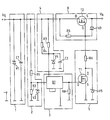
- a protective circuit according to the invention for example in the form of an adapter between a power source and a device to be protected, which is not shown in the drawing, contains the following circuit blocks: Input stage 1 and this downstream voltage divider 2 and a parallel to the voltage divider 2 and this downstream comparator 3 and its associated supply 4 as well as a first electronic switch 5 connected downstream of the comparator and a second electronic switch 6 arranged between the input and output of the protective circuit, which is from the first switch 5 is controlled.
- the input stage 1 contains a transient protection diode V1 and a capacitor C1 connected in parallel to it.
- the voltage divider 2 contains two resistors R1 and R2 connected in series and a transient protection diode V2 connected in parallel with the resistor R2, the voltage across the resistor R2 being fed to the input of the comparator 3 as the output of the voltage divider 2.
- the comparator 3 is a commercially available component, here also designated D1.
- a resistor R8 is connected between its output and the negative potential of the protective circuit.
- the comparator D1 is supplied from the plus potential of the protective circuit via the resistors R3 and R4 connected in parallel, the Supply voltage at the comparator D1 is stabilized by a transient protection diode V4 and protected against voltage pulses and is supported by a capacitor C2 connected in parallel.
- a field effect transistor T1 is provided as the first electronic switch 5, the G connection, also called a gate, directly with the output of the comparator D1, the S connection, also called a source, and the D connection, also called a drain , are connected to the negative potential via a transient protection diode V5.
- a field-effect transistor T2 is also provided as the second electronic switch 6, the D and S connections connecting the input and the output of the protective circuit and the G connection via a resistor R5 to the D connection and via a transient protection diode V3 is connected to the S terminal and to the D terminal of the first switch 5 via a resistor R6 assigned to the first switch 5 in this example.
- the output voltage of the voltage divider 2 or the input voltage of the comparator D1 exceeds the internal one Reference voltage of the comparator D1
- a voltage is conducted at the output of the comparator D1, which turns the field effect transistor T1 on.
- the D terminal of the field effect transistor T1 subsequently pulls the G terminal of the field effect transistor T2 to a lower voltage level via the resistor R6, as a result of which the field effect transistor T2 becomes high-resistance.
- the transient protection diode V3 becomes conductive in the forward direction and thus discharges capacitances (not shown) acting at the output of the protection circuit via the resistor R6 and the field effect transistor T1.
- the transient protection diode V3 also ideally protects the gate-source path of the field-effect transistor T2.
- the transient protection diode V5 limits overshoots when the load is switched off and at the same time protects the field effect transistor T1 against impermissible overvoltages at the D connection. If the field effect transistor T2 is short-circuited, the transient protection diode V5 has a limiting effect on an output voltage U A of the protective circuit and thus protects the load, in which case the transient protection diode V5 is short-circuited in the event of a fault.
- the output voltage U A is switched to zero at a predetermined input overvoltage, which is present, for example, for longer than 1.5 ⁇ s.
- a predetermined input overvoltage which is present, for example, for longer than 1.5 ⁇ s.
- the supply is switched through to the output of the protective circuit by, as in normal operation, no output signal appearing on the comparator D1 and thus the field effect transistor T1 assumes the blocking state and consequently the gate of the field effect transistor T2 keeps it conductive via the resistor R5.
- the voltage drop across the drain-source path from the field-effect transistor T2 is, for example, approximately 4 volts.
Landscapes
- Emergency Protection Circuit Devices (AREA)
- Protection Of Static Devices (AREA)
Abstract
Description
Die Erfindung betrifft eine Ausgleichs- und Ueberspannungsschutzschaltung für elektronische Geräte, insbesondere bei einer Bremseinrichtung eines Schienenfahrzeuges.The invention relates to a compensation and overvoltage protection circuit for electronic devices, in particular in a braking device of a rail vehicle.
Aus der Praxis sind verschiedene Begrenzerschaltungen zum Schutz vor Ueberspannungen bekannt, welche beim Auftreten einer bestimmten Störung ein Gerät abschalten oder die Stromzufuhr unterbrechen. Nach Wegfall der Störung sind die Begrenzerschaltungen entweder zu ersetzen, z.B. Sicherungen, oder manuell wieder einzuschalten, z.B. Schütz.Various limiting circuits for protecting against overvoltages are known in practice, which switch off a device or interrupt the power supply when a specific fault occurs. After the fault has disappeared, the limiter circuits must either be replaced, e.g. Fuses, or manually switch on again, e.g. Contactor.
Die Erfindung, wie sie in den Ansprüchen gekennzeichnet ist, löst die Aufgabe, eine Ausgleichs- und Ueberspannungsschutzschaltung für elektronische Geräte zu schaffen, welche einen einfachen Schaltungsaufbau aufweist und mit der das Gerät gegen Störungen und Zerstörungen, verursacht durch Ausgleichs- und Ueberspannungen in der Speisung, geschützt und nach Wegfall der Störung automatisch wieder an die Speisung zugeschaltet wird.The invention, as characterized in the claims, solves the problem of creating a compensation and overvoltage protection circuit for electronic devices, which has a simple circuit structure and with which the device against interference and destruction caused by compensation and overvoltages in the supply , is protected and is automatically switched back on to the power supply after the fault has disappeared.
Die durch die Erfindung erreichten Vorteile sind im wesentlichen darin zu sehen, dass die Schutzschaltung praktisch von der Störleistung unabhängig ist sowie im Störungsfall einen geringen Leistungsbedarf aufweist. Nachfolgend wird anhand einer einzigen Zeichnung, welche ein Schaltungsschema darstellt, ein Ausführungsbeispiel der Erfindung erläutert.The advantages achieved by the invention can be seen essentially in the fact that the protective circuit is practically independent of the interference power and has a low power requirement in the event of a fault. An exemplary embodiment of the invention is explained below on the basis of a single drawing, which represents a circuit diagram.
Gemäss der einzigen Zeichnung enthält eine erfindungsgemässe Schutzschaltung, beispielsweise als Adapter zwischen einer Stromquelle und einem zu schützenden Gerät, welche in der Zeichnung nicht dargestellt sind, ausgebildet, die nachfolgenden Schaltungsblöcke: Eine parallel zum Eingang geschaltete und als Hochspannungsbegrenzer ausgebildete Eingangsstufe 1, einen parallel zur Eingangsstufe 1 und dieser nachgeschalteten Spannungsteiler 2 und einen parallel zum Spannungsteiler 2 und diesem nachgeschalteten Komparator 3 und seiner zugehörigen Speisung 4 sowie einen dem Komparator nachgeschalteten ersten elektronischen Schalter 5 und einen zwischen Eingang und Ausgang der Schutzschaltung angeordneten zweiten elektronischen Schalter 6, welcher vom ersten Schalter 5 gesteuert wird.According to the single drawing, a protective circuit according to the invention, for example in the form of an adapter between a power source and a device to be protected, which is not shown in the drawing, contains the following circuit blocks: Input stage 1 and this
Die Eingangsstufe 1 enthält eine Transientenschutzdiode V1 und einen dazu parallel geschalteten Kondensator C1. Der Spannungsteiler 2 enthält zwei in Serie geschaltete Widerstände R1 und R2 und eine parallel zum Widerstand R2 geschaltete Transientenschutzdiode V2, wobei die Spannung über dem Widerstand R2 als Ausgang des Spannungsteilers 2 dem Eingang des Komparators 3 zugeleitet wird. Der Komparator 3 ist ein handelsübliches Bauteil, hier auch mit D1 bezeichnet. Zwischen seinem Ausgang und dem Negativpotential der Schutzschaltung ist ein Widerstand R8 geschaltet. Die Speisung des Komparators D1 erfolgt vom Pluspotential der Schutzschaltung über die parallel geschalteten Widerstände R3 und R4, wobei die Speisespannung am Komparator D1 durch eine Transientenschutzdiode V4 stabilisiert und gegenüber Spannungsimpulse geschützt sowie durch einen parallel geschalteten Kondensator C2 gestützt wird. Als ersten elektronischen Schalter 5 ist beispielsweise ein Feldeffekt-Transistor T1 vorgesehen, wobei der G-Anschluss, auch Gate genannt, mit dem Ausgang des Komparators D1, der S-Anschluss, auch Source genannt, direkt und der D-Anschluss, auch Drain genannt, über eine Transientenschutzdiode V5 mit dem Negativpotential verbunden sind. Als zweiter elektronischer Schalter 6 ist ebenfalls ein Feldeffekt-Transistor T2 vorgesehen, wobei die D- und S-Anschlüsse den Eingang und den Ausgang der Schutzschaltung verbinden und der G-Anschluss über einen Widerstand R5 mit dem D-Anschluss und über eine Transientenschutzdiode V3 mit dem S-Anschluss sowie über einen in diesem Beispiel zum ersten Schalter 5 zugeordneten Widerstand R6 mit dem D-Anschluss des ersten Schalters 5 verbunden ist.The input stage 1 contains a transient protection diode V1 and a capacitor C1 connected in parallel to it. The
Daraus ergibt sich folgende Wirkungsweise: Alle Spannungen über der Durchbruchsspannung der Transientenschutzdiode V1, deren theoretische Reaktionszeit beispielsweise bei 1ps liegt, werden je nach Ableitstrom auf einen zulässigen Spannungspegel begrenzt. Der Kondensator C1 in der Eingangsstufe 1 wirkt zusammen mit der Leitungsinduktivität und dem Innenwiderstand der nicht dargestellten Stromquelle als Filter gegen Störspannungen mit hohen Frequenzen, wobei die Grenzfrequenz hauptsächlich durch die Induktivität der Zuleitung bestimmt wird. Ueber den Spannungsteiler R1 und R2 wird dem Komparator D1 ein Eingangssignal zugeführt. Ueberschreitet die Ausgangsspannung des Spannungsteilers 2 bzw. die Eingangsspannung des Komparators D1 die interne Referenzspannung des Komparators D1, wird am Ausgang des Komparators D1 eine Spannung geführt, welche den Feldeffekt-Transistor T1 leitend schaltet. Der D-Anschluss des Feldeffekt-Transistors T1 zieht in der Folge über den Widerstand R6 den G-Anschluss des Feldeffekt-Transistors T2 auf einen tieferen Spannungspegel, wodurch der Feldeffekt-Transistor T2 hochohmig wird. Die Transientenschutzdiode V3 wird in Vorwärtsrichtung leitend und entlädt damit nicht dargestellte, am Ausgang der Schutzschaltung wirkende Kapazitäten über den Widerstand R6 und den Feldeffekt-Transistor T1. Die Transientenschutzdiode V3 schützt dabei in idealer Weise auch die Gate-Source-Strecke des Feldeffekt-Transistors T2.This results in the following mode of operation: All voltages above the breakdown voltage of the transient protection diode V1, the theoretical response time of which is, for example, 1ps, are limited to a permissible voltage level depending on the leakage current. The capacitor C1 in the input stage 1, together with the line inductance and the internal resistance of the current source, not shown, acts as a filter against interference voltages with high frequencies, the cutoff frequency being mainly determined by the inductance of the supply line. An input signal is fed to the comparator D1 via the voltage divider R1 and R2. If the output voltage of the
Die Transientenschutzdiode V5 begrenzt Ueberschwingungen beim Ausschalten der Last und schützt zugleich den Feldeffekt-Transistor T1 vor unzulässigen Ueberspannungen am D-Anschluss. Bei einem Kurzschluss vom Feldeffekt-Transistor T2 wirkt die Transientenschutzdiode V5 begrenzend auf eine Ausgangsspannung UA der Schutzschaltung und schützt damit die Last, wobei in diesem Fehlerfall die Transientenschutzdiode V5 kurzgeschlossen wird.The transient protection diode V5 limits overshoots when the load is switched off and at the same time protects the field effect transistor T1 against impermissible overvoltages at the D connection. If the field effect transistor T2 is short-circuited, the transient protection diode V5 has a limiting effect on an output voltage U A of the protective circuit and thus protects the load, in which case the transient protection diode V5 is short-circuited in the event of a fault.
Die Ausgangsspannung UA wird bei einer vorgegebenen Eingangs-Ueberspannung, welche beispielsweise länger als 1.5 µs ansteht, auf Null geschaltet. Sobald eine Eingangsspannung UE wieder auf den zulässigen Pegel abfällt, wird die Speisung auf den Ausgang der Schutzschaltung durchgeschaltet, indem wie im normalen Betriebsfall, am Komparator D1 kein Ausgangssignal erscheint und somit der Feldeffekt-Transistor T1 den Sperrzustand einnimmt und in der Folge das Gate des Feldeffekt-Transistors T2 diesen über den Widerstand R5 leitend hält. Der Spannungsabfall über die Drain-Source-Strecke vom Feldeffekt-Transistor T2 beträgt beispielsweise ca. 4 Volt.The output voltage U A is switched to zero at a predetermined input overvoltage, which is present, for example, for longer than 1.5 μs. As soon as an input voltage U E drops again to the permissible level, the supply is switched through to the output of the protective circuit by, as in normal operation, no output signal appearing on the comparator D1 and thus the field effect transistor T1 assumes the blocking state and consequently the gate of the field effect transistor T2 keeps it conductive via the resistor R5. The voltage drop across the drain-source path from the field-effect transistor T2 is, for example, approximately 4 volts.
Claims (8)
- eine als Hochspannungsbegrenzer ausgebildete und parallel zum Eingang der Schutzschaltung geschaltete Eingangsstufe (1),
- einen der Eingangsstufe (1) parallel nachgeschalteten Spannungsteiler (2),
- einen dem Spannungsteiler (2) nachgeschalteten Komparator (3), dessen Eingang mit dem Ausgang des Spannungsteilers (2) verbunden ist,
- eine stabilisierte, überspannungsgeschützte Speisung (4) für den Komparator (3) und
- einen ersten und einen zweiten elektronischen Schalter (5 und 6), wobei der erste Schalter (5), dessen Schalteingang mit dem Ausgang des Komparators (3) verbunden ist, im Schaltkreis des zweiten Schalters (6) und der zweite Schalter (6) zwischen Eingang und Ausgang der Schutzschaltung angeordnet sind.1. compensation and overvoltage protection circuit for electronic devices, in particular in a braking device of a rail vehicle, characterized by
an input stage (1) designed as a high-voltage limiter and connected in parallel with the input of the protective circuit,
- one of the input stage (1) connected in parallel voltage divider (2),
a comparator (3) connected downstream of the voltage divider (2), the input of which is connected to the output of the voltage divider (2),
- A stabilized, surge-protected supply (4) for the comparator (3) and
- A first and a second electronic switch (5 and 6), the first switch (5), whose switching input is connected to the output of the comparator (3), in the circuit of the second switch (6) and the second switch (6) are arranged between the input and output of the protective circuit.
Applications Claiming Priority (2)
| Application Number | Priority Date | Filing Date | Title |
|---|---|---|---|
| CH259788 | 1988-07-07 | ||
| CH2597/88 | 1988-07-07 |
Publications (1)
| Publication Number | Publication Date |
|---|---|
| EP0349750A1 true EP0349750A1 (en) | 1990-01-10 |
Family
ID=4237352
Family Applications (1)
| Application Number | Title | Priority Date | Filing Date |
|---|---|---|---|
| EP89109564A Ceased EP0349750A1 (en) | 1988-07-07 | 1989-05-26 | Protection circuit against compensation and overvoltages for electronic equipment |
Country Status (2)
| Country | Link |
|---|---|
| EP (1) | EP0349750A1 (en) |
| AU (1) | AU617832B2 (en) |
Cited By (8)
| Publication number | Priority date | Publication date | Assignee | Title |
|---|---|---|---|---|
| EP0436778A3 (en) * | 1990-01-11 | 1991-11-13 | Vdo Adolf Schindling Ag | Circuit for the protection of a consumer |
| WO2005013453A1 (en) * | 2003-07-28 | 2005-02-10 | Siemens Aktiengesellschaft | Device for the protection of electronic modules against short circuits in a multivoltage on-board electrical wiring system |
| WO2008080576A1 (en) * | 2006-12-29 | 2008-07-10 | Phoenix Contact Gmbh & Co. Kg | Voltage protection arrangement for an electronic device |
| WO2010110946A1 (en) * | 2009-03-24 | 2010-09-30 | General Electric Company | Protecting ballast circuitry against miswiring |
| EP2555367A1 (en) * | 2011-08-05 | 2013-02-06 | Siemens Aktiengesellschaft | Arc fault protective circuit with excess voltage protection |
| DE102013005657A1 (en) | 2013-02-05 | 2014-08-07 | Dehn + Söhne Gmbh + Co. Kg | Device for overvoltage protection by discharging of transient noise from power supply network, provides variable impedance that displace transient disturbances into non-conducting off state, when voltage from supply network is low |
| WO2014195395A3 (en) * | 2013-06-06 | 2015-01-29 | Kongsberg Defence & Aerospace As | Transient protection filter circuit that uses a voltage divider to minimize the effects of thermal runaway |
| DE102008051514B4 (en) | 2008-10-14 | 2022-08-25 | Robert Bosch Gmbh | Voltage monitoring arrangement for a security module |
Citations (5)
| Publication number | Priority date | Publication date | Assignee | Title |
|---|---|---|---|---|
| FR2548839A1 (en) * | 1983-07-08 | 1985-01-11 | Peugeot | Control and/or monitoring installation comprising a device for protecting consumers of power, and for the supply line to these consumers |
| DE3402222A1 (en) * | 1984-01-24 | 1985-07-25 | Licentia Patent-Verwaltungs-Gmbh, 6000 Frankfurt | Circuit arrangement for limiting overvoltages |
| WO1986002786A1 (en) * | 1984-10-24 | 1986-05-09 | Om Ahuja | Auto-reset circuit breaker |
| WO1987000700A1 (en) * | 1985-07-23 | 1987-01-29 | Robert Bosch Gmbh | Over-voltage protection circuit |
| DE3425235C1 (en) * | 1984-07-14 | 1992-03-12 | bso Steuerungstechnik GmbH, 6603 Sulzbach | Circuit arrangement for protecting electronic circuits against overvoltage |
Family Cites Families (1)
| Publication number | Priority date | Publication date | Assignee | Title |
|---|---|---|---|---|
| DE3003382A1 (en) * | 1980-01-31 | 1981-08-06 | Licentia Patent-Verwaltungs-Gmbh, 6000 Frankfurt | METHOD FOR PROTECTING A DC VOLTAGE CONVERTER FROM TOO HIGH VOLTAGES |
-
1989
- 1989-05-26 EP EP89109564A patent/EP0349750A1/en not_active Ceased
- 1989-07-06 AU AU37926/89A patent/AU617832B2/en not_active Ceased
Patent Citations (5)
| Publication number | Priority date | Publication date | Assignee | Title |
|---|---|---|---|---|
| FR2548839A1 (en) * | 1983-07-08 | 1985-01-11 | Peugeot | Control and/or monitoring installation comprising a device for protecting consumers of power, and for the supply line to these consumers |
| DE3402222A1 (en) * | 1984-01-24 | 1985-07-25 | Licentia Patent-Verwaltungs-Gmbh, 6000 Frankfurt | Circuit arrangement for limiting overvoltages |
| DE3425235C1 (en) * | 1984-07-14 | 1992-03-12 | bso Steuerungstechnik GmbH, 6603 Sulzbach | Circuit arrangement for protecting electronic circuits against overvoltage |
| WO1986002786A1 (en) * | 1984-10-24 | 1986-05-09 | Om Ahuja | Auto-reset circuit breaker |
| WO1987000700A1 (en) * | 1985-07-23 | 1987-01-29 | Robert Bosch Gmbh | Over-voltage protection circuit |
Cited By (13)
| Publication number | Priority date | Publication date | Assignee | Title |
|---|---|---|---|---|
| EP0436778A3 (en) * | 1990-01-11 | 1991-11-13 | Vdo Adolf Schindling Ag | Circuit for the protection of a consumer |
| WO2005013453A1 (en) * | 2003-07-28 | 2005-02-10 | Siemens Aktiengesellschaft | Device for the protection of electronic modules against short circuits in a multivoltage on-board electrical wiring system |
| US7675726B2 (en) | 2003-07-28 | 2010-03-09 | Siemens Aktiengesellschaft | Device for protecting electronic modules in a multi-voltage on-board electrical system against short circuits |
| CN104466919A (en) * | 2006-12-29 | 2015-03-25 | 菲尼克斯电气公司 | Voltage protection arrangement for an electronic device |
| WO2008080576A1 (en) * | 2006-12-29 | 2008-07-10 | Phoenix Contact Gmbh & Co. Kg | Voltage protection arrangement for an electronic device |
| US8284531B2 (en) | 2006-12-29 | 2012-10-09 | Phoenix Contact Gmbh & Co. Kg | Voltage protection arrangement for an electronic device |
| CN104466919B (en) * | 2006-12-29 | 2018-11-06 | 菲尼克斯电气公司 | Voltage protection for electronic equipment |
| DE102008051514B4 (en) | 2008-10-14 | 2022-08-25 | Robert Bosch Gmbh | Voltage monitoring arrangement for a security module |
| US8324812B2 (en) | 2009-03-24 | 2012-12-04 | General Electric Company | Protecting ballast circuitry against miswiring |
| WO2010110946A1 (en) * | 2009-03-24 | 2010-09-30 | General Electric Company | Protecting ballast circuitry against miswiring |
| EP2555367A1 (en) * | 2011-08-05 | 2013-02-06 | Siemens Aktiengesellschaft | Arc fault protective circuit with excess voltage protection |
| DE102013005657A1 (en) | 2013-02-05 | 2014-08-07 | Dehn + Söhne Gmbh + Co. Kg | Device for overvoltage protection by discharging of transient noise from power supply network, provides variable impedance that displace transient disturbances into non-conducting off state, when voltage from supply network is low |
| WO2014195395A3 (en) * | 2013-06-06 | 2015-01-29 | Kongsberg Defence & Aerospace As | Transient protection filter circuit that uses a voltage divider to minimize the effects of thermal runaway |
Also Published As
| Publication number | Publication date |
|---|---|
| AU3792689A (en) | 1990-01-11 |
| AU617832B2 (en) | 1991-12-05 |
Similar Documents
| Publication | Publication Date | Title |
|---|---|---|
| DE60130146T2 (en) | ESD PROTECTION | |
| DE2638178C2 (en) | Protection device for integrated circuits against overvoltages | |
| DE69329484T2 (en) | Control electrode shutdown circuit for a power transistor | |
| DE2407333A1 (en) | OVERVOLTAGE PROTECTION | |
| DE69410929T2 (en) | Surge protection circuit | |
| EP0769815A2 (en) | Circuit configuration with protection means | |
| EP0349750A1 (en) | Protection circuit against compensation and overvoltages for electronic equipment | |
| EP1565974B1 (en) | Circuit for protecting integrated circuits against electrostatic discharges | |
| DE19852453A1 (en) | Method for protecting chips for mixed signals against electrostatic discharge | |
| DE4428115C2 (en) | Control unit with a circuit arrangement for protecting the control unit when the control unit mass is interrupted | |
| DE3422995C1 (en) | Surge protection circuit arrangement for telecommunication lines, in particular telephone lines | |
| DE19811269C1 (en) | Electronic circuit with protective circuit for lubrication controllers in motor vehicles, esp. lorries | |
| DE2423646A1 (en) | SURGE ARRESTERS | |
| DE69426935T2 (en) | Electronic semiconductor circuit with surge protection | |
| EP0505602A1 (en) | Protection circuit for the electrical system of a vehicle | |
| EP0348587A2 (en) | Operating failure monitoring circuitry for an electronic apparatus constituting an integrated circuit | |
| EP0135893B1 (en) | Process signal converter for machine tool control | |
| EP0025853A1 (en) | Circuit arrangement for excess-voltage protection | |
| DE3519791A1 (en) | Protection circuit against overload and short-circuit | |
| EP0607875B1 (en) | Protective circuit arrangement | |
| EP0581110B1 (en) | Circuit arrangement for reducing overvoltages on transistors | |
| DE2503406A1 (en) | PROTECTIVE CIRCUIT FOR AMPLIFIER | |
| DE19526493A1 (en) | Method for controlling a load circuit | |
| DE3732861A1 (en) | Circuit arrangement for the protection of low-resistance outputs | |
| DE2302127A1 (en) | OVERVOLTAGE PROTECTION FOR THE OUTPUT OF A STABILIZED POWER SUPPLY DEVICE |
Legal Events
| Date | Code | Title | Description |
|---|---|---|---|
| PUAI | Public reference made under article 153(3) epc to a published international application that has entered the european phase |
Free format text: ORIGINAL CODE: 0009012 |
|
| AK | Designated contracting states |
Kind code of ref document: A1 Designated state(s): CH DE FR GB IT LI NL |
|
| 17P | Request for examination filed |
Effective date: 19900303 |
|
| RAP1 | Party data changed (applicant data changed or rights of an application transferred) |
Owner name: OERLIKON-KNORR EISENBAHNTECHNIK AG |
|
| 17Q | First examination report despatched |
Effective date: 19920127 |
|
| STAA | Information on the status of an ep patent application or granted ep patent |
Free format text: STATUS: THE APPLICATION HAS BEEN REFUSED |
|
| 18R | Application refused |
Effective date: 19921101 |