US8324508B2 - Composite circuit board - Google Patents
Composite circuit board Download PDFInfo
- Publication number
- US8324508B2 US8324508B2 US12/679,653 US67965309A US8324508B2 US 8324508 B2 US8324508 B2 US 8324508B2 US 67965309 A US67965309 A US 67965309A US 8324508 B2 US8324508 B2 US 8324508B2
- Authority
- US
- United States
- Prior art keywords
- conductive line
- line
- internal
- layer
- circuit board
- Prior art date
- Legal status (The legal status is an assumption and is not a legal conclusion. Google has not performed a legal analysis and makes no representation as to the accuracy of the status listed.)
- Expired - Fee Related, expires
Links
Images


Classifications
-
- H—ELECTRICITY
- H05—ELECTRIC TECHNIQUES NOT OTHERWISE PROVIDED FOR
- H05K—PRINTED CIRCUITS; CASINGS OR CONSTRUCTIONAL DETAILS OF ELECTRIC APPARATUS; MANUFACTURE OF ASSEMBLAGES OF ELECTRICAL COMPONENTS
- H05K1/00—Printed circuits
- H05K1/02—Details
- H05K1/0213—Electrical arrangements not otherwise provided for
- H05K1/0237—High frequency adaptations
- H05K1/0248—Skew reduction or using delay lines
-
- H—ELECTRICITY
- H05—ELECTRIC TECHNIQUES NOT OTHERWISE PROVIDED FOR
- H05K—PRINTED CIRCUITS; CASINGS OR CONSTRUCTIONAL DETAILS OF ELECTRIC APPARATUS; MANUFACTURE OF ASSEMBLAGES OF ELECTRICAL COMPONENTS
- H05K1/00—Printed circuits
- H05K1/02—Details
- H05K1/0213—Electrical arrangements not otherwise provided for
- H05K1/0237—High frequency adaptations
- H05K1/0245—Lay-out of balanced signal pairs, e.g. differential lines or twisted lines
-
- H—ELECTRICITY
- H05—ELECTRIC TECHNIQUES NOT OTHERWISE PROVIDED FOR
- H05K—PRINTED CIRCUITS; CASINGS OR CONSTRUCTIONAL DETAILS OF ELECTRIC APPARATUS; MANUFACTURE OF ASSEMBLAGES OF ELECTRICAL COMPONENTS
- H05K1/00—Printed circuits
- H05K1/02—Details
- H05K1/14—Structural association of two or more printed circuits
- H05K1/141—One or more single auxiliary printed circuits mounted on a main printed circuit, e.g. modules, adapters
-
- H—ELECTRICITY
- H05—ELECTRIC TECHNIQUES NOT OTHERWISE PROVIDED FOR
- H05K—PRINTED CIRCUITS; CASINGS OR CONSTRUCTIONAL DETAILS OF ELECTRIC APPARATUS; MANUFACTURE OF ASSEMBLAGES OF ELECTRICAL COMPONENTS
- H05K1/00—Printed circuits
- H05K1/02—Details
- H05K1/14—Structural association of two or more printed circuits
- H05K1/147—Structural association of two or more printed circuits at least one of the printed circuits being bent or folded, e.g. by using a flexible printed circuit
-
- H—ELECTRICITY
- H05—ELECTRIC TECHNIQUES NOT OTHERWISE PROVIDED FOR
- H05K—PRINTED CIRCUITS; CASINGS OR CONSTRUCTIONAL DETAILS OF ELECTRIC APPARATUS; MANUFACTURE OF ASSEMBLAGES OF ELECTRICAL COMPONENTS
- H05K2201/00—Indexing scheme relating to printed circuits covered by H05K1/00
- H05K2201/09—Shape and layout
- H05K2201/09209—Shape and layout details of conductors
- H05K2201/09218—Conductive traces
- H05K2201/09236—Parallel layout
-
- H—ELECTRICITY
- H05—ELECTRIC TECHNIQUES NOT OTHERWISE PROVIDED FOR
- H05K—PRINTED CIRCUITS; CASINGS OR CONSTRUCTIONAL DETAILS OF ELECTRIC APPARATUS; MANUFACTURE OF ASSEMBLAGES OF ELECTRICAL COMPONENTS
- H05K2201/00—Indexing scheme relating to printed circuits covered by H05K1/00
- H05K2201/09—Shape and layout
- H05K2201/09209—Shape and layout details of conductors
- H05K2201/09372—Pads and lands
- H05K2201/09409—Multiple rows of pads, lands, terminals or dummy patterns; Multiple rows of mounted components
-
- H—ELECTRICITY
- H05—ELECTRIC TECHNIQUES NOT OTHERWISE PROVIDED FOR
- H05K—PRINTED CIRCUITS; CASINGS OR CONSTRUCTIONAL DETAILS OF ELECTRIC APPARATUS; MANUFACTURE OF ASSEMBLAGES OF ELECTRICAL COMPONENTS
- H05K2201/00—Indexing scheme relating to printed circuits covered by H05K1/00
- H05K2201/09—Shape and layout
- H05K2201/09209—Shape and layout details of conductors
- H05K2201/09372—Pads and lands
- H05K2201/09481—Via in pad; Pad over filled via
-
- H—ELECTRICITY
- H05—ELECTRIC TECHNIQUES NOT OTHERWISE PROVIDED FOR
- H05K—PRINTED CIRCUITS; CASINGS OR CONSTRUCTIONAL DETAILS OF ELECTRIC APPARATUS; MANUFACTURE OF ASSEMBLAGES OF ELECTRICAL COMPONENTS
- H05K2201/00—Indexing scheme relating to printed circuits covered by H05K1/00
- H05K2201/09—Shape and layout
- H05K2201/09209—Shape and layout details of conductors
- H05K2201/09654—Shape and layout details of conductors covering at least two types of conductors provided for in H05K2201/09218 - H05K2201/095
- H05K2201/09672—Superposed layout, i.e. in different planes
-
- H—ELECTRICITY
- H05—ELECTRIC TECHNIQUES NOT OTHERWISE PROVIDED FOR
- H05K—PRINTED CIRCUITS; CASINGS OR CONSTRUCTIONAL DETAILS OF ELECTRIC APPARATUS; MANUFACTURE OF ASSEMBLAGES OF ELECTRICAL COMPONENTS
- H05K3/00—Apparatus or processes for manufacturing printed circuits
- H05K3/30—Assembling printed circuits with electric components, e.g. with resistors
- H05K3/32—Assembling printed circuits with electric components, e.g. with resistors electrically connecting electric components or wires to printed circuits
- H05K3/34—Assembling printed circuits with electric components, e.g. with resistors electrically connecting electric components or wires to printed circuits by soldering
- H05K3/341—Surface mounted components
- H05K3/3431—Leadless components
- H05K3/3436—Leadless components having an array of bottom contacts, e.g. pad grid array or ball grid array components
Definitions
- a differential transmission line structure as an internal line structure of a packaging component for mounting and sealing a fast-operating semiconductor device such as IC and LSI or a surface-mount type electronic component.
- a differential transmission line structure of conventional design a pair of signal conductors are arranged side by side on a main surface of a dielectric substrate serving as a support and as an insulator as well.
- Conventional differential transmission line structures are typically designed in the form of a parallel microstrip line, and more specifically a structure in which signal conductors are arranged side by side on a main surface of a dielectric substrate, or the form of a parallel strip line in which such a parallel arrangement of signal conductors assumes an internal layer pattern.
- a parallel microstrip line and more specifically a structure in which signal conductors are arranged side by side on a main surface of a dielectric substrate, or the form of a parallel strip line in which such a parallel arrangement of signal conductors assumes an internal layer pattern.
- a pair of signal lines designed in internal layer pattern are led out to a substrate main surface via a through conductor. This makes it possible to establish electrical connection with an electrode terminal of a mounting circuit board.
- An object of the invention is to provide a composite circuit board capable of reducing quality degradation of signals to be transmitted under a condition where a dielectric substrate formed with broadside-coupled strip lines is mounted on a mounting dielectric substrate.
- a composite circuit board in accordance with one embodiment of the invention comprises a first circuit board and a second circuit board.
- the first circuit board includes a first conductive line and a second conductive line which is longer in length than the first conductive line.
- the second circuit board includes a third conductive line which is electrically connected to the first conductive line and a fourth conductive line which is electrically connected to the second conductive line and is shorter in length than the third conductive line.
- FIG. 1 is a perspective view showing a composite circuit board in accordance with one embodiment of the invention
- FIG. 2 is a plan view of the composite circuit board shown in FIG. 1 ;
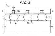
- FIG. 3 is a front view of the composite circuit board shown in FIG. 1 ;
- FIG. 4 is a side view of the composite circuit board shown in FIG. 1 .
- a composite circuit board 1 comprises a package 2 (a first circuit board) and a mounting board 3 (a second circuit board).
- a package 2 a first circuit board
- a mounting board 3 a second circuit board
- circular connection pads 4 attached to the package 2 (a first end and a second end)
- circular connection pads 5 attached to the mounting board 3 (a third end and a fourth end).
- the circular connection pad 4 and the circular connection pad 5 are electrically connected to each other by a solder ball 12 .
- the package 2 is the first circuit board having a dielectric layer 6 and an internal layered conductive line pair 7 .
- the mounting board 3 is the second circuit board having a resin substrate 8 and a surface-layer line pair 9 .
- the internal layered conductive line pair 7 includes an internal layered conductive line 7 b acting as the first conductive line and an internal layered conductive line 7 a acting as the second conductive line, thereby constituting a differential transmission line structure.
- the internal layered conductive line 7 b is composed of an internal-layer line 11 a acting as a first internal layered conductive line, a land 11 b , and a through conductor 11 c acting as a first through conductor.
- the internal layered conductive line 7 a is composed of an internal-layer line 10 a acting as a second internal layered conductive line, a land 10 b , and a through conductor 10 c acting as a second through conductor.
- the internal layered conductive line pair 7 which is disposed inside the dielectric layer 6 , is built as broadside-coupled strip lines opposed to each other in a thickness direction of the package 2 .
- the internal-layer line 10 a and the internal-layer line 11 a are opposed to each other in the thickness direction, with a dielectric body interposed therebetween, and are so arranged as to overlap each other when viewed from the top face of the package 2 .
- the internal-layer line 10 a and the internal-layer line 11 a are arranged in line layers having different levels inside the dielectric layer 6 . Therefore, the vertical line portion of the internal layered conductive line 7 a composed of the land 10 b and the through conductor 10 c and the vertical line portion of the internal layered conductive line 7 b composed of the land 11 b and the through conductor 11 c differ in length from each other.
- the vertical line portion composed of the land 11 b and the through conductor 11 c is made short.
- the vertical line portion composed of the land 10 b and the through conductor 10 c is made long.
- connection pads 4 are arranged side by side in an extending direction of the internal-layer line 10 a and the internal-layer line 11 a , it follows that the internal-layer line 10 a is made longer than the internal-layer line 11 a.
- the “length” of a line refers to a distance from one external power input-output portion to the other external power input-output portion thereof.
- the length of the internal layered conductive line 7 b acting as the first conductive line is the sum of the length of the through conductor 11 c which is a distance from the connection pad 4 acting as the external power input-output portion to the semiconductor device mounting land 11 b and the length of the internal-layer line 11 a which is a distance from a boundary between the land 11 b and the internal-layer line 11 a to a part of connection with the semiconductor device.
- connection pads 5 connected with the surface-layer line pair 9 are arranged side by side in an extending direction of the surface-layer line 9 a and the surface-layer line 9 b .
- the surface-layer line 9 a is connected to a connection pad 5 a (the fourth end) situated toward the front as seen in the extending direction
- the surface-layer line 9 b is connected to a connection pad 5 b (the third end) situated toward the rear as seen in the extending direction.
- the surface-layer line 9 b and the connection pad 5 b constitute the third conductive line
- the surface-layer line 9 a and the connection pad 5 a constitute the fourth conductive line.
- the attainment of the broadside-coupled strip line entails the difference in length between the internal layered conductive line 7 a and the internal layered conductive line 7 b due to their different levels.
- the surface-layer line 9 a and the surface-layer line 9 b differ in length from each other due to the positional difference between the connection pad 5 a and the connection pad 5 b.
- the wording “substantially equal” means that the difference between the sums of length falls within 5% of the pulse width of an electric signal transmitted through the first to fourth conductive lines (or the period of analog waves).
- the third conductive line 9 b , and the fourth conductive line 9 a are made of the same material, the sums of the line lengths of them are substantially equal.
- the sum of the length of the first conductive line and that of the third conductive line and the sum of the length of the second conductive line and that of the fourth conductive line are substantially equal. In this case, quality degradation of signals can be reduced more reliably.
Landscapes
- Engineering & Computer Science (AREA)
- Microelectronics & Electronic Packaging (AREA)
- Structure Of Printed Boards (AREA)
- Combinations Of Printed Boards (AREA)
Abstract
Description
Claims (8)
Applications Claiming Priority (3)
| Application Number | Priority Date | Filing Date | Title |
|---|---|---|---|
| JP2008-088851 | 2008-03-28 | ||
| JP2008088851 | 2008-03-28 | ||
| PCT/JP2009/056390 WO2009119849A1 (en) | 2008-03-28 | 2009-03-27 | Composite wiring board |
Publications (2)
| Publication Number | Publication Date |
|---|---|
| US20100206625A1 US20100206625A1 (en) | 2010-08-19 |
| US8324508B2 true US8324508B2 (en) | 2012-12-04 |
Family
ID=41114035
Family Applications (1)
| Application Number | Title | Priority Date | Filing Date |
|---|---|---|---|
| US12/679,653 Expired - Fee Related US8324508B2 (en) | 2008-03-28 | 2009-03-27 | Composite circuit board |
Country Status (3)
| Country | Link |
|---|---|
| US (1) | US8324508B2 (en) |
| JP (1) | JP4927993B2 (en) |
| WO (1) | WO2009119849A1 (en) |
Families Citing this family (5)
| Publication number | Priority date | Publication date | Assignee | Title |
|---|---|---|---|---|
| US9379424B2 (en) * | 2014-05-08 | 2016-06-28 | Fujitsu Limited | Compensation for length differences in vias associated with differential signaling |
| DE202014008844U1 (en) | 2014-11-06 | 2014-11-24 | Rosenberger Hochfrequenztechnik Gmbh & Co. Kg | Electrical interface |
| WO2018025697A1 (en) * | 2016-08-02 | 2018-02-08 | 株式会社村田製作所 | Multilayered substrate |
| JP7454996B2 (en) * | 2020-05-11 | 2024-03-25 | CIG Photonics Japan株式会社 | optical module |
| US20230240001A1 (en) * | 2020-07-02 | 2023-07-27 | Nippon Telegraph And Telephone Corporation | Wiring Board and Signal Connecting Structure |
Citations (7)
| Publication number | Priority date | Publication date | Assignee | Title |
|---|---|---|---|---|
| JPH01286493A (en) | 1988-05-13 | 1989-11-17 | Hitachi Ltd | Multilayer wiring board |
| US20020179335A1 (en) * | 1999-08-26 | 2002-12-05 | International Business Machines Corporation | Method for filling high aspect ratio via holes in electronic substrates and the resulting holes |
| JP2005011627A (en) | 2003-06-18 | 2005-01-13 | Fujitsu Component Ltd | Contact module and connector device including the same |
| US20050040846A1 (en) | 2003-07-28 | 2005-02-24 | Kanji Otsuka | Signal transmission system, and signal transmission line |
| US20060202318A1 (en) * | 2005-03-09 | 2006-09-14 | Matsushita Electric Industrial Co., Ltd. | Imaging module and method for forming the same |
| US20070194433A1 (en) * | 2004-03-19 | 2007-08-23 | Renesas Technology Corp. | Electronic circuit, a semiconductor device and a mounting substrate |
| US7417195B2 (en) * | 2002-08-07 | 2008-08-26 | Denso Corporation | Circuit board and circuit board connection structure |
Family Cites Families (3)
| Publication number | Priority date | Publication date | Assignee | Title |
|---|---|---|---|---|
| JP2004349406A (en) * | 2003-05-21 | 2004-12-09 | Konica Minolta Business Technologies Inc | Differential transmission circuit and image processor using the same |
| JP2005277028A (en) * | 2004-03-24 | 2005-10-06 | Mitsubishi Electric Corp | High-speed transmission board structure |
| JP4150977B2 (en) * | 2004-09-30 | 2008-09-17 | 株式会社村田製作所 | Wiring pattern structure of differential transmission path |
-
2009
- 2009-03-27 US US12/679,653 patent/US8324508B2/en not_active Expired - Fee Related
- 2009-03-27 JP JP2010505872A patent/JP4927993B2/en not_active Expired - Fee Related
- 2009-03-27 WO PCT/JP2009/056390 patent/WO2009119849A1/en not_active Ceased
Patent Citations (9)
| Publication number | Priority date | Publication date | Assignee | Title |
|---|---|---|---|---|
| JPH01286493A (en) | 1988-05-13 | 1989-11-17 | Hitachi Ltd | Multilayer wiring board |
| US20020179335A1 (en) * | 1999-08-26 | 2002-12-05 | International Business Machines Corporation | Method for filling high aspect ratio via holes in electronic substrates and the resulting holes |
| US7417195B2 (en) * | 2002-08-07 | 2008-08-26 | Denso Corporation | Circuit board and circuit board connection structure |
| JP2005011627A (en) | 2003-06-18 | 2005-01-13 | Fujitsu Component Ltd | Contact module and connector device including the same |
| US20050040846A1 (en) | 2003-07-28 | 2005-02-24 | Kanji Otsuka | Signal transmission system, and signal transmission line |
| JP2005051496A (en) | 2003-07-28 | 2005-02-24 | Kanji Otsuka | Signal transmission system and signal transmission line |
| US7190188B2 (en) | 2003-07-28 | 2007-03-13 | Kanji Otsuka | Signal transmission system, and signal transmission line |
| US20070194433A1 (en) * | 2004-03-19 | 2007-08-23 | Renesas Technology Corp. | Electronic circuit, a semiconductor device and a mounting substrate |
| US20060202318A1 (en) * | 2005-03-09 | 2006-09-14 | Matsushita Electric Industrial Co., Ltd. | Imaging module and method for forming the same |
Non-Patent Citations (1)
| Title |
|---|
| International Search Report for corresponding International application PCT/JP2009/056390. |
Also Published As
| Publication number | Publication date |
|---|---|
| JPWO2009119849A1 (en) | 2011-07-28 |
| JP4927993B2 (en) | 2012-05-09 |
| WO2009119849A1 (en) | 2009-10-01 |
| US20100206625A1 (en) | 2010-08-19 |
Similar Documents
| Publication | Publication Date | Title |
|---|---|---|
| JP5582168B2 (en) | High frequency signal line | |
| CN103379733B (en) | Printed wiring board, semiconductor package part and printed circuit board (PCB) | |
| JP4653005B2 (en) | Electronic component package | |
| US9059493B2 (en) | High-frequency signal line and electronic device | |
| US8324508B2 (en) | Composite circuit board | |
| JP5323435B2 (en) | Multi-layer wiring board for differential transmission | |
| US8531023B2 (en) | Substrate for semiconductor package and method of manufacturing thereof | |
| JP2009111132A (en) | Multilayer wiring board | |
| JP3872413B2 (en) | Semiconductor device | |
| JP2016171191A (en) | Wiring board | |
| JP2008270363A (en) | High frequency package | |
| JP2006042098A (en) | High frequency wiring board | |
| JP2002185201A (en) | High frequency wiring board | |
| JP7455730B2 (en) | wiring board | |
| JP7325303B2 (en) | wireless module | |
| WO2016149269A1 (en) | Comprehensive layout strategy for flip chipping integrated circuits | |
| JP4377725B2 (en) | High frequency wiring board | |
| JP3798978B2 (en) | Multilayer wiring board | |
| JP5286694B2 (en) | Electronic equipment | |
| JP2005286436A (en) | High frequency wiring board | |
| JP5193780B2 (en) | Connection structure for differential transmission | |
| JP2024048912A (en) | Wiring board, wiring structure using wiring board, package for mounting electronic components, and electronic module | |
| JP2005064220A (en) | Wiring board | |
| WO2025126853A1 (en) | Multilayer substrate | |
| JP2004260377A (en) | Balun transformer |
Legal Events
| Date | Code | Title | Description |
|---|---|---|---|
| AS | Assignment |
Owner name: KYOCERA CORPORATION, JAPAN Free format text: ASSIGNMENT OF ASSIGNORS INTEREST;ASSIGNOR:MAETANI, MARAKI;REEL/FRAME:024125/0881 Effective date: 20100319 |
|
| ZAAA | Notice of allowance and fees due |
Free format text: ORIGINAL CODE: NOA |
|
| ZAAB | Notice of allowance mailed |
Free format text: ORIGINAL CODE: MN/=. |
|
| STCF | Information on status: patent grant |
Free format text: PATENTED CASE |
|
| FEPP | Fee payment procedure |
Free format text: PAYOR NUMBER ASSIGNED (ORIGINAL EVENT CODE: ASPN); ENTITY STATUS OF PATENT OWNER: LARGE ENTITY Free format text: PAYER NUMBER DE-ASSIGNED (ORIGINAL EVENT CODE: RMPN); ENTITY STATUS OF PATENT OWNER: LARGE ENTITY |
|
| FPAY | Fee payment |
Year of fee payment: 4 |
|
| MAFP | Maintenance fee payment |
Free format text: PAYMENT OF MAINTENANCE FEE, 8TH YEAR, LARGE ENTITY (ORIGINAL EVENT CODE: M1552); ENTITY STATUS OF PATENT OWNER: LARGE ENTITY Year of fee payment: 8 |
|
| FEPP | Fee payment procedure |
Free format text: MAINTENANCE FEE REMINDER MAILED (ORIGINAL EVENT CODE: REM.); ENTITY STATUS OF PATENT OWNER: LARGE ENTITY |
|
| LAPS | Lapse for failure to pay maintenance fees |
Free format text: PATENT EXPIRED FOR FAILURE TO PAY MAINTENANCE FEES (ORIGINAL EVENT CODE: EXP.); ENTITY STATUS OF PATENT OWNER: LARGE ENTITY |
|
| STCH | Information on status: patent discontinuation |
Free format text: PATENT EXPIRED DUE TO NONPAYMENT OF MAINTENANCE FEES UNDER 37 CFR 1.362 |
|
| FP | Lapsed due to failure to pay maintenance fee |
Effective date: 20241204 |