US8309966B2 - Gate driver on array of a display - Google Patents

Gate driver on array of a display Download PDF

Info

Publication number
US8309966B2
US8309966B2 US12/898,727 US89872710A US8309966B2 US 8309966 B2 US8309966 B2 US 8309966B2 US 89872710 A US89872710 A US 89872710A US 8309966 B2 US8309966 B2 US 8309966B2
Authority
US
United States
Prior art keywords
gate driver
electrode
array
display
drain electrode
Prior art date
Legal status (The legal status is an assumption and is not a legal conclusion. Google has not performed a legal analysis and makes no representation as to the accuracy of the status listed.)
Active, expires
Application number
US12/898,727
Other versions
US20110018001A1 (en
Inventor
Tung-Chang Tsai
Lee-Hsun Chang
Ming-Chang Shih
Jing-Ru Chen
Kuei-Sheng Tseng
Current Assignee (The listed assignees may be inaccurate. Google has not performed a legal analysis and makes no representation or warranty as to the accuracy of the list.)
AU Optronics Corp
Original Assignee
AU Optronics Corp
Priority date (The priority date is an assumption and is not a legal conclusion. Google has not performed a legal analysis and makes no representation as to the accuracy of the date listed.)
Filing date
Publication date
Application filed by AU Optronics Corp filed Critical AU Optronics Corp
Priority to US12/898,727 priority Critical patent/US8309966B2/en
Assigned to AU OPTRONICS CORP. reassignment AU OPTRONICS CORP. ASSIGNMENT OF ASSIGNORS INTEREST (SEE DOCUMENT FOR DETAILS). Assignors: TSENG, KUEI-SHENG, CHANG, LEE-HSUN, CHEN, JING-RU, SHIH, MING-CHANG, TSAI, TUNG-CHANG
Publication of US20110018001A1 publication Critical patent/US20110018001A1/en
Application granted granted Critical
Publication of US8309966B2 publication Critical patent/US8309966B2/en
Active legal-status Critical Current
Adjusted expiration legal-status Critical

Links

Images

Classifications

    • HELECTRICITY
    • H01ELECTRIC ELEMENTS
    • H01LSEMICONDUCTOR DEVICES NOT COVERED BY CLASS H10
    • H01L27/00Devices consisting of a plurality of semiconductor or other solid-state components formed in or on a common substrate
    • H01L27/02Devices consisting of a plurality of semiconductor or other solid-state components formed in or on a common substrate including semiconductor components specially adapted for rectifying, oscillating, amplifying or switching and having at least one potential-jump barrier or surface barrier; including integrated passive circuit elements with at least one potential-jump barrier or surface barrier
    • H01L27/12Devices consisting of a plurality of semiconductor or other solid-state components formed in or on a common substrate including semiconductor components specially adapted for rectifying, oscillating, amplifying or switching and having at least one potential-jump barrier or surface barrier; including integrated passive circuit elements with at least one potential-jump barrier or surface barrier the substrate being other than a semiconductor body, e.g. an insulating body
    • H01L27/1214Devices consisting of a plurality of semiconductor or other solid-state components formed in or on a common substrate including semiconductor components specially adapted for rectifying, oscillating, amplifying or switching and having at least one potential-jump barrier or surface barrier; including integrated passive circuit elements with at least one potential-jump barrier or surface barrier the substrate being other than a semiconductor body, e.g. an insulating body comprising a plurality of TFTs formed on a non-semiconducting substrate, e.g. driving circuits for AMLCDs
    • H01L27/1259Multistep manufacturing methods
    • H01L27/1288Multistep manufacturing methods employing particular masking sequences or specially adapted masks, e.g. half-tone mask
    • HELECTRICITY
    • H01ELECTRIC ELEMENTS
    • H01LSEMICONDUCTOR DEVICES NOT COVERED BY CLASS H10
    • H01L27/00Devices consisting of a plurality of semiconductor or other solid-state components formed in or on a common substrate
    • H01L27/02Devices consisting of a plurality of semiconductor or other solid-state components formed in or on a common substrate including semiconductor components specially adapted for rectifying, oscillating, amplifying or switching and having at least one potential-jump barrier or surface barrier; including integrated passive circuit elements with at least one potential-jump barrier or surface barrier
    • H01L27/12Devices consisting of a plurality of semiconductor or other solid-state components formed in or on a common substrate including semiconductor components specially adapted for rectifying, oscillating, amplifying or switching and having at least one potential-jump barrier or surface barrier; including integrated passive circuit elements with at least one potential-jump barrier or surface barrier the substrate being other than a semiconductor body, e.g. an insulating body
    • H01L27/1214Devices consisting of a plurality of semiconductor or other solid-state components formed in or on a common substrate including semiconductor components specially adapted for rectifying, oscillating, amplifying or switching and having at least one potential-jump barrier or surface barrier; including integrated passive circuit elements with at least one potential-jump barrier or surface barrier the substrate being other than a semiconductor body, e.g. an insulating body comprising a plurality of TFTs formed on a non-semiconducting substrate, e.g. driving circuits for AMLCDs
    • YGENERAL TAGGING OF NEW TECHNOLOGICAL DEVELOPMENTS; GENERAL TAGGING OF CROSS-SECTIONAL TECHNOLOGIES SPANNING OVER SEVERAL SECTIONS OF THE IPC; TECHNICAL SUBJECTS COVERED BY FORMER USPC CROSS-REFERENCE ART COLLECTIONS [XRACs] AND DIGESTS
    • Y10TECHNICAL SUBJECTS COVERED BY FORMER USPC
    • Y10STECHNICAL SUBJECTS COVERED BY FORMER USPC CROSS-REFERENCE ART COLLECTIONS [XRACs] AND DIGESTS
    • Y10S438/00Semiconductor device manufacturing: process
    • Y10S438/942Masking

Definitions

  • the present invention relates to a gate driving circuit of a display, and a method of fabricating a device of a display, and more particularly, to a pull-down module of a gate driver on array (GOA) having high pull-down ability, and a method of making a device of a display capable of avoiding metal loss.
  • GOA gate driver on array
  • FIG. 1 illustrates a circuit diagram of a gate driving circuit of a display.
  • the gate driving circuit is used to generate pulse signals according to a predetermined timing sequence, and the pulse signals are delivered to gate lines so as to control switching of the thin film transistors (TFTs) in the pixel regions of the display.
  • the gate driving circuit mainly includes a plurality of signal lines (e.g. L 1 , L 2 , L 3 and L 4 ), and a plurality of TFTs (e.g. T 1 , T 2 , T 3 and T 4 ).
  • the signal line L 1 is used to deliver a voltage signal Vss
  • the signal line L 2 is used to deliver a start pulse signal Vst
  • the signal line L 3 is used to deliver a complementary clock signal Vxck
  • the signal line L 4 is used to deliver a clock signal Vck.
  • the TFT T 1 serves as a starting switch
  • the TFT T 2 serves as a pulse switch.
  • the start pulse signal Vst turns on the TFT T 1
  • the TFT T 2 is also turned on so that clock signal Vck can pass and provide a voltage signal V N to the N th gate line of the display panel.
  • the TFTs T 3 , T 4 serve as a pull-down module, which pulls down the voltage of the signal delivered to the gate line to a reference voltage, i.e. the level of the voltage signal Vss, for example ⁇ 6V. Specifically, the TFT T 4 can pull down the voltage of the node Q 1 to the level of the voltage signal Vss, and the TFT T 3 can pull down the voltage of the node Q 2 to the level of the voltage signal Vss.
  • the conventional TFTs T 3 , T 4 cannot provide pull-down effect when turned off.
  • the start pulse voltage Vst or the clock signal Vck may have abnormal waveform during this period of time, and consequently the TFTs of the pixel regions may be turned on falsely.
  • the pull-down ability of the conventional pull-down module requires to be improved.
  • the size of the metal pattern actually formed is usually found smaller than its original designed size. This is so called metal loss, and the metal loss problem is serious particularly in patterning the second metal layer (Metal 2 ).
  • This metal loss problem influences the reliability of the TFTs of pixel regions, the TFTs of gate driver on array (GOA), and other components e.g. photo spacer stages.
  • a method of forming a device of a display includes the following steps. First of all, a substrate is provided. Then, a first conductive layer on the substrate, and patterned to form a first conductive structure. An insulating layer, a semiconductor layer, an ohmic contact layer, a second conductive layer, and a photoresist pattern are consecutively formed on the first conductive structure.
  • the photoresist pattern includes a first thickness region, and a second thickness region outside the first thickness region, and a thickness of the second thickness region is smaller than a thickness of the first thickness region.
  • a gate driver on array of a display includes a substrate, and a gate driver on array structure.
  • the substrate includes a peripheral region.
  • the gate driver on array structure is disposed in the peripheral region.
  • the gate driver on array structure includes a pull-down transistor, and the pull-down transistor includes a gate electrode, an insulating layer, a semiconductor island, a source electrode, and a drain electrode.
  • the semiconductor island extends out of both edges of the gate electrode, and extends out of an edge of the source electrode and an edge of the drain electrode.
  • the semiconductor island of the pull-down transistor of the display extends out of the gate electrode, and also the source electrode and the drain electrode, and thus improves the pull-down ability.
  • the method of the present invention uses a photoresist pattern with different thickness to perform photolithographic and etching processes for forming the pull-down transistor and photo spacer stage of the display, and therefore metal loss problem is diminished.
  • FIG. 1 illustrates a circuit diagram of a gate driving circuit of a display.
  • FIGS. 2-6 illustrate a method of forming a photo spacer stage of a display according to a preferred embodiment of the present invention.
  • FIGS. 7-13 illustrate a method of forming a pull-down transistor of a GOA of a display according to another embodiment of the present invention.
  • FIGS. 14-20 illustrate a method of forming a pixel transistor of a display according to another embodiment of the present invention.
  • FIGS. 21-23 illustrate a GOA of a display according to a preferred embodiment of the present invention.
  • FIGS. 2-6 illustrate a method of forming a photo spacer stage of a display according to a preferred embodiment of the present invention.
  • a substrate 10 is provided.
  • the substrate 10 is a thin film transistor substrate (TFT substrate) of an LCD panel, but not limited.
  • TFT substrate thin film transistor substrate
  • a first conductive layer is formed on the substrate 10 , and the first conductive layer is patterned by photolithographic and etching techniques to form a first conductive structure 12 .
  • an insulating layer 14 , a semiconductor layer 16 , an ohmic contact layer 18 , a second conductive layer 20 and a photoresist pattern 22 are consecutively formed on the first conductive structure 12 .
  • the first conductive structure 12 and the second conductive layer 20 are made of metal material.
  • the photoresist pattern 22 includes a first thickness region 22 A, and a second thickness region 22 B outside the first thickness region 22 A, where the thickness of the second thickness region 22 B is smaller than the thickness of the first thickness region 22 A.
  • the thickness of the first thickness region 22 A is substantially between 1.5 and 2.5 microns
  • the thickness of the second thickness region 22 B is substantially between 5000 and 6000 angstroms, but not limited.
  • the photoresist pattern 22 may be patterned by exposing with a graytone mask such as a halftone mask or a phase shift mask, but not limited.
  • the photoresist pattern 22 is used as an etching mask to perform a wet etching process on a part of the second conductive layer 20 not covered by the photoresist pattern 22 , and another part of the second conductive layer 20 covered by the photoresist pattern 22 is remained.
  • an ashing (photoresist ashing, PR ashing) process is implemented to partially remove the photoresist material to thin or to reduce the thickness of the photoresist pattern 22 .
  • the thickness of the second thickness region 22 B is still smaller than the thickness of the first thickness region 22 A.
  • the thickness of the second thickness region 22 B of the photoresist pattern 22 is reduced to avoid metal loss of the second conductive layer 20 , but the dimension of the photoresist pattern 22 is not changed.
  • the ashing process may be carried out by dry etching, for instance, and the dimension and thickness of the second thickness region 22 B may be changed.
  • the dimension of the second thickness region 22 B of the photoresist pattern 22 can be reduced, or the second thickness region 22 B may be removed so as to control the metal loss.
  • a dry etching process is performed using the photoresist pattern 22 and the second conductive layer 20 as an etching mask to dry etch a part of the ohmic contact layer 18 and a part of the semiconductor layer 16 not covered by the photoresist pattern 22 and the second conductive layer 20 .
  • a PR strip process is performed by e.g. dry etching or wet etching to remove the photoresist pattern 22 . Accordingly, a photo spacer stage 24 composed of the first conductive structure 12 , the insulating layer 14 , the semiconductor layer 16 , the ohmic contact layer 18 and the second conductive layer 22 stacked up is formed.
  • FIGS. 7-13 illustrate a method of forming a pull-down transistor of a gate driver on array (GOA) of a display according to another embodiment of the present invention.
  • the GOA is a gate driving circuit formed on the substrate of the display.
  • a substrate 30 is provided.
  • a first conductive layer is formed on the substrate 30 , and patterned by photolithographic and etching techniques to form a first conductive structure 32 which serves as a gate electrode.
  • an insulating layer 34 , a semiconductor layer 36 , an ohmic contact layer 38 , a second conductive layer 40 , and a photoresist pattern 42 are consecutively formed on the first conductive structure 32 .
  • the first conductive structure 32 and the second conductive layer 40 are made of metal material, and the insulating layer 34 serves as a gate insulating layer.
  • the photoresist pattern 42 includes a first thickness region 42 A, a second thickness region 42 B outside the first thickness region 42 A, and a third thickness region 42 C substantially corresponding to a central part of the first conductive structure 32 .
  • the thickness of the second thickness region 42 B and the thickness of the third thickness region 42 C are smaller than the thickness of the first thickness region 42 A, and the thickness of the second thickness region 42 B and the thickness of the third thickness region 42 C are approximately the same, but not limited.
  • the thickness of the first thickness region 42 A is substantially between 1.5 and 2.5 microns
  • the thickness of the second thickness region 42 B and the third thickness region 42 C are both substantially between 5000 and 6000 angstroms, but not limited.
  • the photoresist pattern 42 may be formed by exposing with a graytone mask such as a halftone mask or a phase shift mask, but not limited.
  • a wet etching process is performed using the photoresist pattern 42 as an etching mask to etch a part of the second conductive layer 40 not covered by the photoresist pattern 42 , while another part of the second conductive layer 40 covered by the photoresist pattern 42 is remained.
  • an ashing process is carried out upon the photoresist pattern 42 to thin a part of the photoresist pattern 42 in the first thickness region 42 A, and to remove another part of the photoresist pattern 42 in the second thickness region 42 B and in the third thickness region 42 C. Accordingly, the second conductive layer 40 is partially exposed after the ashing process.
  • the photoresist pattern 42 in the second thickness region 42 B and in the third thickness region 42 C is entirely removed, so that the semiconductor layer 36 can extend out with respect to other layers in successive process.
  • the ashing process can be modified to change the dimension or thickness of the second thickness region 42 B and the third thickness region 42 C based on different considerations. For example, the photoresist pattern 42 in the second thickness region 42 B and the third thickness region 42 C can be shrank or thinned in the ashing process, instead of being entirely removed.
  • the second conductive layer 40 is used as an etching mask to dry etch a part of the ohmic contact layer 38 and a part of the semiconductor layer 36 not covered by the second conductive layer 40 .
  • the photoresist pattern 42 is used as an etching mask to dry etch at least part of the second conductive layer 40 not covered by the photoresist pattern 42 .
  • the etched part of the second conductive layer 40 includes a part of the second conductive layer 40 outside the first thickness region 42 A (corresponding to the original second thickness region 42 B), and a part of the second conductive layer 40 between the first thickness region 42 A (corresponding to the original third thickness region 42 C).
  • the remaining second conductive layer 40 forms a source electrode 40 A and a drain electrode 40 B, and the ohmic contact layer 38 and the semiconductor layer 36 extend out of the edge of the second conductive layer 40 .
  • the outer edges of the source electrode 40 A and the drain electrode 40 B in a horizontal direction extend out of the first conductive structure 32 which is disposed under the second conductive layer 40 and serves as a gate electrode.
  • the dimension of the gate electrode is smaller than the dimension of the source electrode 40 A and the drain electrode 40 B.
  • the source electrode 40 A and the drain electrode 40 B may also draw back from the edges of the first conductive structure 32 .
  • the dimension of the gate electrode may be greater than the dimension of the source electrode 40 A and the drain electrode 40 B.
  • a part of the ohmic contact layer 38 not covered by the second conductive layer 40 is dry etched using the photoresist pattern 42 as an etching mask so that the shape of the ohmic contact layer 38 and the shape of the source electrode 40 A and the drain electrode are corresponsive, while the semiconductor layer 36 remains extending out of the second conductive layer 40 .
  • a small portion of the semiconductor layer 36 may be etched, but most of the semiconductor layer 36 remains and serves as a channel of the TFT.
  • the photoresist pattern 42 is removed, and a pull-down transistor 44 of a GOA of a display composed of the first conductive structure (gate electrode) 32 , the insulating layer 34 , the semiconductor layer 36 , the ohmic contact layer 38 , the source electrode 40 A and the drain electrode 40 B is formed on the substrate 30 .
  • FIGS. 14-20 illustrate a method of forming a pixel transistor of a display according to another embodiment of the present invention.
  • a substrate 50 is provided.
  • a first conductive layer is formed on the substrate 50 , and patterned by photolithographic and etching techniques to form a first conductive structure 52 which serves as a gate electrode.
  • an insulating layer 54 is formed on the substrate 50 , and patterned by photolithographic and etching techniques to form a first conductive structure 52 which serves as a gate electrode.
  • an insulating layer 54 , a semiconductor layer 56 , an ohmic contact layer 58 , a second conductive layer 60 , and a photoresist pattern 62 are consecutively formed on the first conductive structure 52 .
  • the first conductive structure 52 and the second conductive layer 60 are made of metal material
  • the insulating layer 54 serves as a gate insulating layer.
  • the photoresist pattern 62 includes a first thickness region 62 A, a second thickness region 62 B outside the first thickness region 62 A, and a third thickness region 62 C substantially corresponding to a central part of the first conductive structure 52 .
  • the thickness of the second thickness region 62 B and the thickness of the third thickness region 62 C are smaller than the thickness of the first thickness region 62 A, and the thickness of the second thickness region 62 B is slightly greater than the thickness of the third thickness region 62 C, but not limited.
  • the thickness of the first thickness region 62 A is substantially between 1.5 and 2.5 microns
  • the thickness of the second thickness region 62 B and the third thickness region 62 C are both substantially between 5000 and 6000 angstroms.
  • the thickness of the photoresist pattern 62 can be modified wherever necessary.
  • the photoresist pattern 62 may be formed by exposing with a graytone mask such as a halftone mask or a phase shift mask, but not limited.
  • a wet etching process is performed using the photoresist pattern 62 as an etching mask to etch a part of the second conductive layer 60 not covered by the photoresist pattern 62 , while another part of the second conductive layer 60 covered by the photoresist pattern 62 is remained.
  • an ashing process is carried out upon the photoresist pattern 62 to thin a part of the photoresist pattern 62 in the first thickness region 62 A and in the second thickness region 62 B, and to remove another part of the photoresist pattern 62 in the third thickness region 62 C.
  • the thickness of the second thickness region 62 B is still smaller than the thickness of the first thickness region 62 A, and the photoresist pattern 62 partially exposes the second conductive layer 60 (i.e. a part of the second conductive layer 60 corresponding to the original third thickness region 62 C).
  • the photoresist pattern 62 in the second thickness region 62 B is not entirely removed, but only the thickness of the second thickness region 62 B is shrank so as to prevent metal loss of the second conductive layer 60 .
  • a part of the ohmic contact layer 58 and a part of the semiconductor layer 56 not covered by the second conductive layer 60 is dry etched using the second conductive layer 60 as an etching mask.
  • a part of the second conductive layer 60 not covered by the first thickness region 62 A and the second thickness region 62 B of the photoresist pattern 62 is dry etched using the photoresist pattern 62 as an etching mask to remove the part of the second conductive layer 60 between the first thickness region 62 A (corresponding to the original third thickness region 62 C) for forming a source electrode 60 A and a drain electrode 60 B.
  • the outer edges of the source electrode 60 A and the drain electrode 60 B in a horizontal direction extend out of the first conductive structure 52 which is disposed under the second conductive layer 60 and serves as a gate electrode.
  • the dimension of the gate electrode is smaller than the dimension of the source electrode 60 A and the drain electrode 60 B.
  • the source electrode 60 A and the drain electrode 60 B may also draw back from the edges of the first conductive structure 52 .
  • the dimension of the gate electrode may be greater than the dimension of the source electrode 60 A and the drain electrode 60 B.
  • the ohmic contact layer 58 is dry etched using the photoresist pattern 62 as an etching mask to remove a part of the ohmic contact layer 58 (not covered by the source electrode 60 A and the drain electrode 60 B) between the first thickness region 62 A so that the shape of the ohmic contact layer 58 and the shape of the source electrode 60 A and the drain electrode 60 B are corresponsive.
  • a small portion of the semiconductor layer 56 may be etched, but most of the semiconductor layer 56 remains and serves as a channel of the TFT.
  • the photoresist pattern 62 is removed, and a pixel transistor 64 of a display composed of the first conductive structure (gate electrode) 52 , the insulating layer 54 , the semiconductor layer 56 , the ohmic contact layer 58 , the source electrode 60 A and the drain electrode 60 B is formed.
  • FIGS. 21-23 illustrate a GOA of a display according to a preferred embodiment of the present invention, where FIG. 21 depicts the display, FIG. 22 depicts the GOA, and FIG. 23 depicts a pull-down transistor.
  • the display 70 e.g. an LCD panel includes a substrate 72 having a peripheral region 74 and a display region 76 as shown in FIG. 21 .
  • the display 70 includes a GOA structure 80 formed in the peripheral region 74 , and the GOA structure 80 includes pull-down transistors T 3 , T 4 . As shown in FIG.
  • the pull-down transistor T 3 (or T 4 ) includes a gate electrode 90 disposed on the substrate 72 , an insulating layer 92 disposed on the substrate 72 and the gate electrode 90 , a semiconductor island 94 disposed on the insulating layer 92 , a source electrode 96 A and a drain electrode 96 B disposed on the semiconductor island 94 .
  • the semiconductor island 94 includes a semiconductor layer 94 A disposed on the insulating layer 92 , and a ohmic contact layer 94 B between the semiconductor layer 94 A, and the source electrode 96 A/drain electrode 96 B.
  • the semiconductor island 94 extends out of the edges of the gate electrode 90 , and the distance between an edge of the semiconductor island 94 and the corresponding edge of the gate electrode 90 is substantially between 2.5 and 3.5 microns. Also, the semiconductor island 94 may extend out of the edge of the source electrode 96 A or the drain electrode 96 B, and the distance between an edge of the semiconductor island 94 and the corresponding edge of the source electrode 96 A, or the distance between an edge of the semiconductor island 94 and the corresponding edge of the drain electrode 96 B is substantially between 4 and 5 microns, preferably but not limited.
  • the GOA structure 80 includes a signal source S 1 , a negative power source S 2 , and nodes Q 1 , Q 2 .
  • the signal source S 1 electrically connects the gate electrode of the pull-down transistors T 3 , T 4 , and delivers clock signal Vck, complementary clock signal Vxck, and the voltage signal V N+1 of the N+1 th to the pull-down transistors T 3 , T 4 .
  • the negative power source S 2 delivers the voltage signal Vss to the source electrode of the pull-down transistors T 3 , T 4 .
  • the node Q 1 is electrically connected to the drain electrode of the pull-down transistor T 4
  • the node Q 2 is electrically connected to the drain electrode of the pull-down transistor T 3 .
  • the semiconductor island extends out of the gate electrode, and also the source electrode and the drain electrode, and thus improves the pull-down ability of the pull-down transistor of the display.
  • the method of the present invention uses a photoresist pattern with different thickness to perform photolithographic and etching processes for forming the pull-down transistor and photo spacer stage of the display, and therefore metal loss problem is diminished.

Abstract

A gate driver on array of a display includes a substrate having a peripheral region, and a gate driver on array structure formed in the peripheral region. The gate driver on array structure includes a pull-down transistor, and the pull-down transistor has a gate electrode, an insulating layer, a semiconductor island, a source electrode, and a drain electrode. The semiconductor island extends out of both edges of the gate electrode, and extends out of an edge of the source electrode and an edge of the drain electrode.

Description

CROSS REFERENCE TO RELATED APPLICATIONS
This application is a division of application Ser. No. 12/206,746 filed on Sep. 9, 2008.
BACKGROUND OF THE INVENTION
1. Field of the Invention
The present invention relates to a gate driving circuit of a display, and a method of fabricating a device of a display, and more particularly, to a pull-down module of a gate driver on array (GOA) having high pull-down ability, and a method of making a device of a display capable of avoiding metal loss.
2. Description of the Prior Art
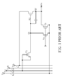
FIG. 1 illustrates a circuit diagram of a gate driving circuit of a display. As shown in FIG. 1, the gate driving circuit is used to generate pulse signals according to a predetermined timing sequence, and the pulse signals are delivered to gate lines so as to control switching of the thin film transistors (TFTs) in the pixel regions of the display. The gate driving circuit mainly includes a plurality of signal lines (e.g. L1, L2, L3 and L4), and a plurality of TFTs (e.g. T1, T2, T3 and T4). The signal line L1 is used to deliver a voltage signal Vss, the signal line L2 is used to deliver a start pulse signal Vst, the signal line L3 is used to deliver a complementary clock signal Vxck, and the signal line L4 is used to deliver a clock signal Vck. The TFT T1 serves as a starting switch, and the TFT T2 serves as a pulse switch. When the start pulse signal Vst turns on the TFT T1, the TFT T2 is also turned on so that clock signal Vck can pass and provide a voltage signal VN to the Nth gate line of the display panel. The TFTs T3, T4 serve as a pull-down module, which pulls down the voltage of the signal delivered to the gate line to a reference voltage, i.e. the level of the voltage signal Vss, for example −6V. Specifically, the TFT T4 can pull down the voltage of the node Q1 to the level of the voltage signal Vss, and the TFT T3 can pull down the voltage of the node Q2 to the level of the voltage signal Vss.
The conventional TFTs T3, T4 cannot provide pull-down effect when turned off. However, the start pulse voltage Vst or the clock signal Vck may have abnormal waveform during this period of time, and consequently the TFTs of the pixel regions may be turned on falsely. Thus, the pull-down ability of the conventional pull-down module requires to be improved.
Also, in the conventional photolithography process of display fabrication, for example 4PEP array processes, the size of the metal pattern actually formed is usually found smaller than its original designed size. This is so called metal loss, and the metal loss problem is serious particularly in patterning the second metal layer (Metal 2). This metal loss problem influences the reliability of the TFTs of pixel regions, the TFTs of gate driver on array (GOA), and other components e.g. photo spacer stages.
SUMMARY OF THE INVENTION
It is therefore one of the objectives of the present invention to provide a gate driver on array of a display, and a method of forming a device of a display to solve the aforementioned problem.
According to the present invention, a method of forming a device of a display is provided. The method includes the following steps. First of all, a substrate is provided. Then, a first conductive layer on the substrate, and patterned to form a first conductive structure. An insulating layer, a semiconductor layer, an ohmic contact layer, a second conductive layer, and a photoresist pattern are consecutively formed on the first conductive structure. The photoresist pattern includes a first thickness region, and a second thickness region outside the first thickness region, and a thickness of the second thickness region is smaller than a thickness of the first thickness region.
According to the present invention, a gate driver on array of a display is also provided. The gate driver on array includes a substrate, and a gate driver on array structure. The substrate includes a peripheral region. The gate driver on array structure is disposed in the peripheral region. The gate driver on array structure includes a pull-down transistor, and the pull-down transistor includes a gate electrode, an insulating layer, a semiconductor island, a source electrode, and a drain electrode. The semiconductor island extends out of both edges of the gate electrode, and extends out of an edge of the source electrode and an edge of the drain electrode.
The semiconductor island of the pull-down transistor of the display extends out of the gate electrode, and also the source electrode and the drain electrode, and thus improves the pull-down ability. In addition, the method of the present invention uses a photoresist pattern with different thickness to perform photolithographic and etching processes for forming the pull-down transistor and photo spacer stage of the display, and therefore metal loss problem is diminished.
These and other objectives of the present invention will no doubt become obvious to those of ordinary skill in the art after reading the following detailed description of the preferred embodiment that is illustrated in the various figures and drawings.
BRIEF DESCRIPTION OF THE DRAWINGS
FIG. 1 illustrates a circuit diagram of a gate driving circuit of a display.
FIGS. 2-6 illustrate a method of forming a photo spacer stage of a display according to a preferred embodiment of the present invention.
FIGS. 7-13 illustrate a method of forming a pull-down transistor of a GOA of a display according to another embodiment of the present invention.
FIGS. 14-20 illustrate a method of forming a pixel transistor of a display according to another embodiment of the present invention.
FIGS. 21-23 illustrate a GOA of a display according to a preferred embodiment of the present invention.
DETAILED DESCRIPTION
FIGS. 2-6 illustrate a method of forming a photo spacer stage of a display according to a preferred embodiment of the present invention. As shown in FIG. 2, a substrate 10 is provided. In this embodiment, the substrate 10 is a thin film transistor substrate (TFT substrate) of an LCD panel, but not limited. Then, a first conductive layer is formed on the substrate 10, and the first conductive layer is patterned by photolithographic and etching techniques to form a first conductive structure 12. Subsequently, an insulating layer 14, a semiconductor layer 16, an ohmic contact layer 18, a second conductive layer 20 and a photoresist pattern 22 are consecutively formed on the first conductive structure 12. In this embodiment, the first conductive structure 12 and the second conductive layer 20 are made of metal material. The photoresist pattern 22 includes a first thickness region 22A, and a second thickness region 22B outside the first thickness region 22A, where the thickness of the second thickness region 22B is smaller than the thickness of the first thickness region 22A. In this embodiment, the thickness of the first thickness region 22A is substantially between 1.5 and 2.5 microns, and the thickness of the second thickness region 22B is substantially between 5000 and 6000 angstroms, but not limited. In addition, the photoresist pattern 22 may be patterned by exposing with a graytone mask such as a halftone mask or a phase shift mask, but not limited.
As shown in FIG. 3, the photoresist pattern 22 is used as an etching mask to perform a wet etching process on a part of the second conductive layer 20 not covered by the photoresist pattern 22, and another part of the second conductive layer 20 covered by the photoresist pattern 22 is remained.
Subsequently, as shown in FIG. 4, an ashing (photoresist ashing, PR ashing) process is implemented to partially remove the photoresist material to thin or to reduce the thickness of the photoresist pattern 22. After the ashing process, the thickness of the second thickness region 22B is still smaller than the thickness of the first thickness region 22A. In this embodiment, the thickness of the second thickness region 22B of the photoresist pattern 22 is reduced to avoid metal loss of the second conductive layer 20, but the dimension of the photoresist pattern 22 is not changed. In other embodiments of the present invention, however, the ashing process may be carried out by dry etching, for instance, and the dimension and thickness of the second thickness region 22B may be changed. For example, the dimension of the second thickness region 22B of the photoresist pattern 22 can be reduced, or the second thickness region 22B may be removed so as to control the metal loss.
As shown in FIG. 5. a dry etching process is performed using the photoresist pattern 22 and the second conductive layer 20 as an etching mask to dry etch a part of the ohmic contact layer 18 and a part of the semiconductor layer 16 not covered by the photoresist pattern 22 and the second conductive layer 20.
As shown in FIG. 6, a PR strip process is performed by e.g. dry etching or wet etching to remove the photoresist pattern 22. Accordingly, a photo spacer stage 24 composed of the first conductive structure 12, the insulating layer 14, the semiconductor layer 16, the ohmic contact layer 18 and the second conductive layer 22 stacked up is formed.
FIGS. 7-13 illustrate a method of forming a pull-down transistor of a gate driver on array (GOA) of a display according to another embodiment of the present invention. The GOA is a gate driving circuit formed on the substrate of the display. As shown in FIG. 7, a substrate 30 is provided. A first conductive layer is formed on the substrate 30, and patterned by photolithographic and etching techniques to form a first conductive structure 32 which serves as a gate electrode. Subsequently, an insulating layer 34, a semiconductor layer 36, an ohmic contact layer 38, a second conductive layer 40, and a photoresist pattern 42 are consecutively formed on the first conductive structure 32. In this embodiment, the first conductive structure 32 and the second conductive layer 40 are made of metal material, and the insulating layer 34 serves as a gate insulating layer. The photoresist pattern 42 includes a first thickness region 42A, a second thickness region 42B outside the first thickness region 42A, and a third thickness region 42C substantially corresponding to a central part of the first conductive structure 32. Preferably, the thickness of the second thickness region 42B and the thickness of the third thickness region 42C are smaller than the thickness of the first thickness region 42A, and the thickness of the second thickness region 42B and the thickness of the third thickness region 42C are approximately the same, but not limited. In this embodiment, the thickness of the first thickness region 42A is substantially between 1.5 and 2.5 microns, the thickness of the second thickness region 42B and the third thickness region 42C are both substantially between 5000 and 6000 angstroms, but not limited. In addition, the photoresist pattern 42 may be formed by exposing with a graytone mask such as a halftone mask or a phase shift mask, but not limited.
As shown in FIG. 8, a wet etching process is performed using the photoresist pattern 42 as an etching mask to etch a part of the second conductive layer 40 not covered by the photoresist pattern 42, while another part of the second conductive layer 40 covered by the photoresist pattern 42 is remained.
As shown in FIG. 9, an ashing process is carried out upon the photoresist pattern 42 to thin a part of the photoresist pattern 42 in the first thickness region 42A, and to remove another part of the photoresist pattern 42 in the second thickness region 42B and in the third thickness region 42C. Accordingly, the second conductive layer 40 is partially exposed after the ashing process. In this embodiment, the photoresist pattern 42 in the second thickness region 42B and in the third thickness region 42C is entirely removed, so that the semiconductor layer 36 can extend out with respect to other layers in successive process. However, the ashing process can be modified to change the dimension or thickness of the second thickness region 42B and the third thickness region 42C based on different considerations. For example, the photoresist pattern 42 in the second thickness region 42B and the third thickness region 42C can be shrank or thinned in the ashing process, instead of being entirely removed.
As shown in FIG. 10, the second conductive layer 40 is used as an etching mask to dry etch a part of the ohmic contact layer 38 and a part of the semiconductor layer 36 not covered by the second conductive layer 40.
Subsequently, as shown in FIG. 11, the photoresist pattern 42 is used as an etching mask to dry etch at least part of the second conductive layer 40 not covered by the photoresist pattern 42. The etched part of the second conductive layer 40 includes a part of the second conductive layer 40 outside the first thickness region 42A (corresponding to the original second thickness region 42B), and a part of the second conductive layer 40 between the first thickness region 42A (corresponding to the original third thickness region 42C). The remaining second conductive layer 40 forms a source electrode 40A and a drain electrode 40B, and the ohmic contact layer 38 and the semiconductor layer 36 extend out of the edge of the second conductive layer 40. In this embodiment, the outer edges of the source electrode 40A and the drain electrode 40B in a horizontal direction extend out of the first conductive structure 32 which is disposed under the second conductive layer 40 and serves as a gate electrode. In other words, the dimension of the gate electrode is smaller than the dimension of the source electrode 40A and the drain electrode 40B. However, the source electrode 40A and the drain electrode 40B may also draw back from the edges of the first conductive structure 32. In other words, the dimension of the gate electrode may be greater than the dimension of the source electrode 40A and the drain electrode 40B.
As shown in FIG. 12, a part of the ohmic contact layer 38 not covered by the second conductive layer 40 is dry etched using the photoresist pattern 42 as an etching mask so that the shape of the ohmic contact layer 38 and the shape of the source electrode 40A and the drain electrode are corresponsive, while the semiconductor layer 36 remains extending out of the second conductive layer 40. In the above etching process, a small portion of the semiconductor layer 36 may be etched, but most of the semiconductor layer 36 remains and serves as a channel of the TFT.
As shown in FIG. 13, the photoresist pattern 42 is removed, and a pull-down transistor 44 of a GOA of a display composed of the first conductive structure (gate electrode) 32, the insulating layer 34, the semiconductor layer 36, the ohmic contact layer 38, the source electrode 40A and the drain electrode 40B is formed on the substrate 30.
FIGS. 14-20 illustrate a method of forming a pixel transistor of a display according to another embodiment of the present invention. As shown in FIG. 14, a substrate 50 is provided. A first conductive layer is formed on the substrate 50, and patterned by photolithographic and etching techniques to form a first conductive structure 52 which serves as a gate electrode. Subsequently, an insulating layer 54, a semiconductor layer 56, an ohmic contact layer 58, a second conductive layer 60, and a photoresist pattern 62 are consecutively formed on the first conductive structure 52. In this embodiment, the first conductive structure 52 and the second conductive layer 60 are made of metal material, and the insulating layer 54 serves as a gate insulating layer. The photoresist pattern 62 includes a first thickness region 62A, a second thickness region 62B outside the first thickness region 62A, and a third thickness region 62C substantially corresponding to a central part of the first conductive structure 52. Preferably, the thickness of the second thickness region 62B and the thickness of the third thickness region 62C are smaller than the thickness of the first thickness region 62A, and the thickness of the second thickness region 62B is slightly greater than the thickness of the third thickness region 62C, but not limited. In this embodiment, the thickness of the first thickness region 62A is substantially between 1.5 and 2.5 microns, the thickness of the second thickness region 62B and the third thickness region 62C are both substantially between 5000 and 6000 angstroms. The thickness of the photoresist pattern 62, however, can be modified wherever necessary. In addition, the photoresist pattern 62 may be formed by exposing with a graytone mask such as a halftone mask or a phase shift mask, but not limited.
As shown in FIG. 15, a wet etching process is performed using the photoresist pattern 62 as an etching mask to etch a part of the second conductive layer 60 not covered by the photoresist pattern 62, while another part of the second conductive layer 60 covered by the photoresist pattern 62 is remained.
As shown in FIG. 16, an ashing process is carried out upon the photoresist pattern 62 to thin a part of the photoresist pattern 62 in the first thickness region 62A and in the second thickness region 62B, and to remove another part of the photoresist pattern 62 in the third thickness region 62C. After the ashing process, the thickness of the second thickness region 62B is still smaller than the thickness of the first thickness region 62A, and the photoresist pattern 62 partially exposes the second conductive layer 60 (i.e. a part of the second conductive layer 60 corresponding to the original third thickness region 62C). In this embodiment, the photoresist pattern 62 in the second thickness region 62B is not entirely removed, but only the thickness of the second thickness region 62B is shrank so as to prevent metal loss of the second conductive layer 60.
As shown in FIG. 17, a part of the ohmic contact layer 58 and a part of the semiconductor layer 56 not covered by the second conductive layer 60 is dry etched using the second conductive layer 60 as an etching mask.
Subsequently, as shown in FIG. 18, a part of the second conductive layer 60 not covered by the first thickness region 62A and the second thickness region 62B of the photoresist pattern 62 is dry etched using the photoresist pattern 62 as an etching mask to remove the part of the second conductive layer 60 between the first thickness region 62A (corresponding to the original third thickness region 62C) for forming a source electrode 60A and a drain electrode 60B. In this embodiment, the outer edges of the source electrode 60A and the drain electrode 60B in a horizontal direction extend out of the first conductive structure 52 which is disposed under the second conductive layer 60 and serves as a gate electrode. In other words, the dimension of the gate electrode is smaller than the dimension of the source electrode 60A and the drain electrode 60B. However, the source electrode 60A and the drain electrode 60B may also draw back from the edges of the first conductive structure 52. In other words, the dimension of the gate electrode may be greater than the dimension of the source electrode 60A and the drain electrode 60B.
As shown in FIG. 19, the ohmic contact layer 58 is dry etched using the photoresist pattern 62 as an etching mask to remove a part of the ohmic contact layer 58 (not covered by the source electrode 60A and the drain electrode 60B) between the first thickness region 62A so that the shape of the ohmic contact layer 58 and the shape of the source electrode 60A and the drain electrode 60B are corresponsive. In the above etching process, a small portion of the semiconductor layer 56 may be etched, but most of the semiconductor layer 56 remains and serves as a channel of the TFT.
As shown in FIG. 20, the photoresist pattern 62 is removed, and a pixel transistor 64 of a display composed of the first conductive structure (gate electrode) 52, the insulating layer 54, the semiconductor layer 56, the ohmic contact layer 58, the source electrode 60A and the drain electrode 60B is formed.
FIGS. 21-23 illustrate a GOA of a display according to a preferred embodiment of the present invention, where FIG. 21 depicts the display, FIG. 22 depicts the GOA, and FIG. 23 depicts a pull-down transistor. The display 70 e.g. an LCD panel includes a substrate 72 having a peripheral region 74 and a display region 76 as shown in FIG. 21. The display 70 includes a GOA structure 80 formed in the peripheral region 74, and the GOA structure 80 includes pull-down transistors T3, T4. As shown in FIG. 23, the pull-down transistor T3 (or T4) includes a gate electrode 90 disposed on the substrate 72, an insulating layer 92 disposed on the substrate 72 and the gate electrode 90, a semiconductor island 94 disposed on the insulating layer 92, a source electrode 96A and a drain electrode 96B disposed on the semiconductor island 94. The semiconductor island 94 includes a semiconductor layer 94A disposed on the insulating layer 92, and a ohmic contact layer 94B between the semiconductor layer 94A, and the source electrode 96A/drain electrode 96B. In this embodiment, the semiconductor island 94 extends out of the edges of the gate electrode 90, and the distance between an edge of the semiconductor island 94 and the corresponding edge of the gate electrode 90 is substantially between 2.5 and 3.5 microns. Also, the semiconductor island 94 may extend out of the edge of the source electrode 96A or the drain electrode 96B, and the distance between an edge of the semiconductor island 94 and the corresponding edge of the source electrode 96A, or the distance between an edge of the semiconductor island 94 and the corresponding edge of the drain electrode 96B is substantially between 4 and 5 microns, preferably but not limited.
As shown in FIG. 22, the GOA structure 80 includes a signal source S1, a negative power source S2, and nodes Q1, Q2. The signal source S1 electrically connects the gate electrode of the pull-down transistors T3, T4, and delivers clock signal Vck, complementary clock signal Vxck, and the voltage signal VN+1 of the N+1th to the pull-down transistors T3, T4. The negative power source S2 delivers the voltage signal Vss to the source electrode of the pull-down transistors T3, T4. The node Q1 is electrically connected to the drain electrode of the pull-down transistor T4, and the node Q2 is electrically connected to the drain electrode of the pull-down transistor T3.
In conclusion, the semiconductor island extends out of the gate electrode, and also the source electrode and the drain electrode, and thus improves the pull-down ability of the pull-down transistor of the display. In addition, the method of the present invention uses a photoresist pattern with different thickness to perform photolithographic and etching processes for forming the pull-down transistor and photo spacer stage of the display, and therefore metal loss problem is diminished.
Those skilled in the art will readily observe that numerous modifications and alterations of the device and method may be made while retaining the teachings of the invention. Accordingly, the above disclosure should be construed as limited only by the metes and bounds of the appended claims.

Claims (12)

1. A gate driver on array of a display, comprising:
a substrate comprising a peripheral region; and
a gate driver on array structure formed in the peripheral region, the gate driver on array structure comprising a pull-down transistor, and the pull-down transistor comprising a gate electrode, an insulating layer, a semiconductor island, a source electrode, and a drain electrode;
wherein the semiconductor island extends out of both edges of the gate electrode and extends out of an edge of the source electrode and an edge of the drain electrode, and a distance between an edge of the semiconductor island extending out of an edge of the gate electrode and the corresponding edge of the gate electrode is substantially between 2.5 and 3.5 microns.
2. The gate driver on array of a display of claim 1, wherein the gate driver on array structure comprises a signal source electrically connected to the drain electrode.
3. The gate driver on array of a display of claim 1, wherein the gate driver on array structure comprises a negative power source electrically connected to the source electrode.
4. The gate driver on array of a display of claim 1, wherein the gate driver on array structure comprises a node electrically connected to the drain electrode.
5. A gate driver on array of a display, comprising:
a substrate comprising a peripheral region; and
a gate driver on array structure formed in the peripheral region, the gate driver on array structure comprising a pull-down transistor, and the pull-down transistor comprising a gate electrode, an insulating layer, a semiconductor island, a source electrode, and a drain electrode;
wherein the semiconductor island extends out of both edges of the gate electrode and extends out of an edge of the source electrode and an edge of the drain electrode, and a distance between an edge of the semiconductor island extending out of the edge of the source electrode and the corresponding edge of the source electrode is substantially between 4 and 5 microns.
6. The gate driver on array of a display of claim 5, wherein the gate driver on array structure comprises a signal source electrically connected to the drain electrode.
7. The gate driver on array of a display of claim 5, wherein the gate driver on array structure comprises a negative power source electrically connected to the source electrode.
8. The gate driver on array of a display of claim 5, wherein the gate driver on array structure comprises a node electrically connected to the drain electrode.
9. A gate driver on array of a display, comprising:
a substrate comprising a peripheral region; and
a gate driver on array structure formed in the peripheral region, the gate driver on array structure comprising a pull-down transistor, and the pull-down transistor comprising a gate electrode, an insulating layer, a semiconductor island, a source electrode, and a drain electrode;
wherein the semiconductor island extends out of both edges of the gate electrode and extends out of an edge of the source electrode and an edge of the drain electrode, and a distance between an edge of the semiconductor island extending out of the edge of the drain electrode and the corresponding edge of the drain electrode is substantially between 4 and 5 microns.
10. The gate driver on array of a display of claim 9, wherein the gate driver on array structure comprises a signal source electrically connected to the drain electrode.
11. The gate driver on array of a display of claim 9, wherein the gate driver on array structure comprises a negative power source electrically connected to the source electrode.
12. The gate driver on array of a display of claim 9, wherein the gate driver on array structure comprises a node electrically connected to the drain electrode.
US12/898,727 2008-04-18 2010-10-06 Gate driver on array of a display Active 2029-01-02 US8309966B2 (en)

Priority Applications (1)

Application Number Priority Date Filing Date Title
US12/898,727 US8309966B2 (en) 2008-04-18 2010-10-06 Gate driver on array of a display

Applications Claiming Priority (5)

Application Number Priority Date Filing Date Title
TW097114245A TWI374510B (en) 2008-04-18 2008-04-18 Gate driver on array of a display and method of making device of a display
TW97114245A 2008-04-18
TW097114245 2008-04-18
US12/206,746 US8053288B2 (en) 2008-04-18 2008-09-09 Method of making device of a display
US12/898,727 US8309966B2 (en) 2008-04-18 2010-10-06 Gate driver on array of a display

Related Parent Applications (1)

Application Number Title Priority Date Filing Date
US12/206,746 Division US8053288B2 (en) 2008-04-18 2008-09-09 Method of making device of a display

Publications (2)

Publication Number Publication Date
US20110018001A1 US20110018001A1 (en) 2011-01-27
US8309966B2 true US8309966B2 (en) 2012-11-13

Family

ID=41200363

Family Applications (2)

Application Number Title Priority Date Filing Date
US12/206,746 Active 2029-06-03 US8053288B2 (en) 2008-04-18 2008-09-09 Method of making device of a display
US12/898,727 Active 2029-01-02 US8309966B2 (en) 2008-04-18 2010-10-06 Gate driver on array of a display

Family Applications Before (1)

Application Number Title Priority Date Filing Date
US12/206,746 Active 2029-06-03 US8053288B2 (en) 2008-04-18 2008-09-09 Method of making device of a display

Country Status (2)

Country Link
US (2) US8053288B2 (en)
TW (1) TWI374510B (en)

Cited By (3)

* Cited by examiner, † Cited by third party
Publication number Priority date Publication date Assignee Title
US20140080253A1 (en) * 2011-01-12 2014-03-20 Semiconductor Energy Laboratory Co., Ltd. Manufacturing method of semiconductor device
US8921948B2 (en) 2011-01-12 2014-12-30 Semiconductor Energy Laboratory Co., Ltd. Semiconductor device and manufacturing method thereof
US10964281B2 (en) 2009-03-26 2021-03-30 Semiconductor Energy Laboratory Co., Ltd. Liquid crystal display device, driving method of the same, and electronic device including the same

Families Citing this family (12)

* Cited by examiner, † Cited by third party
Publication number Priority date Publication date Assignee Title
TWI374510B (en) * 2008-04-18 2012-10-11 Au Optronics Corp Gate driver on array of a display and method of making device of a display
JP5839896B2 (en) 2010-09-09 2016-01-06 株式会社半導体エネルギー研究所 Display device
US20120227328A1 (en) 2011-03-10 2012-09-13 David Link pet door enclosure system
CN103018991B (en) * 2012-12-24 2015-01-28 京东方科技集团股份有限公司 Array substrate, manufacturing method thereof and display device
CN103489879B (en) * 2013-10-11 2016-04-20 京东方科技集团股份有限公司 Array base palte and preparation method thereof, display unit
US9704888B2 (en) 2014-01-08 2017-07-11 Apple Inc. Display circuitry with reduced metal routing resistance
CN103901690A (en) * 2014-03-20 2014-07-02 京东方科技集团股份有限公司 Array substrate, manufacturing method of array substrate and display device
CN105118419B (en) * 2015-09-28 2017-11-10 深圳市华星光电技术有限公司 A kind of display device, TFT substrate and GOA drive circuits
CN107134460B (en) * 2017-04-11 2019-08-02 深圳市华星光电半导体显示技术有限公司 Display device and its GOA circuit
CN111223459B (en) 2018-11-27 2022-03-08 元太科技工业股份有限公司 Shift register and gate drive circuit
CN109976049A (en) * 2019-04-08 2019-07-05 深圳市华星光电半导体显示技术有限公司 Display panel and preparation method thereof
CN112068372A (en) * 2020-09-10 2020-12-11 深圳市华星光电半导体显示技术有限公司 Array substrate and display panel

Citations (27)

* Cited by examiner, † Cited by third party
Publication number Priority date Publication date Assignee Title
US4459739A (en) * 1981-05-26 1984-07-17 Northern Telecom Limited Thin film transistors
JPH02219239A (en) * 1989-02-20 1990-08-31 Semiconductor Energy Lab Co Ltd Manufacture of thin film transistor
JPH02219240A (en) * 1989-02-20 1990-08-31 Semiconductor Energy Lab Co Ltd Manufacture of thin film transistor
US5949502A (en) * 1995-08-07 1999-09-07 Hitachi, Ltd. Liquid crystal device having resistor elements
US6255130B1 (en) 1998-11-19 2001-07-03 Samsung Electronics Co., Ltd. Thin film transistor array panel and a method for manufacturing the same
US20010019125A1 (en) 1999-12-31 2001-09-06 Hong Mun-Pyo Contact structures of wirings and methods for manufacturing the same, and thin film transistor array panels including the same and methods for manufacturing the same
US6459124B1 (en) * 1996-10-02 2002-10-01 Semiconductor Energy Laboratory Co., Ltd. Semiconductor device and process for manufacturing the same, and electronic device
US6562645B2 (en) * 2000-06-29 2003-05-13 Boe-Hydis Technology Co, Ltd. Method of fabricating fringe field switching mode liquid crystal display
US6849873B2 (en) 1999-04-08 2005-02-01 Samsung Electronics Co., Ltd. Thin film transistor array panel for a liquid crystal display
US6876428B2 (en) 2001-06-08 2005-04-05 Lg Philips Lcd Co., Ltd. Method of manufacturing a liquid crystal display panel using a gray tone mask
US20050142681A1 (en) 2003-12-29 2005-06-30 Jae-Moon Soh Mask and method of manufacturing liquid crystal display device using the same
US6924869B2 (en) * 2003-04-29 2005-08-02 Au Optronics Corporation Display panel with the integrated driver circuit
US20050263768A1 (en) 2004-05-27 2005-12-01 Lg. Philips Lcd Co., Ltd. Liquid crystal display device and fabricating method thereof
US20060008932A1 (en) 2004-04-06 2006-01-12 Kum-Mi Oh Liquid crystal display device having driving circuit and method of fabricating the same
US20060017681A1 (en) * 2004-06-30 2006-01-26 Jang Yong H Liquid crystal display device and method for fabricating the same
US20060022199A1 (en) 2004-07-27 2006-02-02 Mitsubishi Denki Kabushiki Kaisha Thin film transistor array substrate and method of producing the same
US20060073645A1 (en) 2004-10-06 2006-04-06 Samsung Electronics Co., Ltd. Manufacturing method of a thin film transistor array panel
US20060175611A1 (en) 2003-07-22 2006-08-10 Nec Lcd Technologies, Ltd. Thin film transistor circuit device, production method thereof and liquid crystal display using the thin film transistor circuit device
US20070138471A1 (en) 2005-12-14 2007-06-21 Lim Kyoung N Liquid crystal display device and method for fabricating the same
TW200727485A (en) 2006-01-06 2007-07-16 Au Optronics Corp Thin film transistor and method for manufacturing the same
US20070164330A1 (en) 2006-01-16 2007-07-19 Samsung Electronics Co., Ltd Display substrate and method of manufacturing the same
US20070216822A1 (en) * 2002-07-17 2007-09-20 Nobuyuki Ishige Liquid crystal display device
US7279371B2 (en) * 2003-12-08 2007-10-09 Samsung Electronics Co., Ltd. Thin film transistor array panel and manufacturing method thereof
US20080003726A1 (en) 2006-06-29 2008-01-03 Lg Philips Lcd Co., Ltd Method for fabricating a thin film transistor for use with a flat panel display device
US7416926B2 (en) * 2004-12-24 2008-08-26 Lg Display Co., Ltd. Liquid crystal display device and method for fabricating the same
US20100026669A1 (en) * 2008-08-01 2010-02-04 Samsung Electronics Co., Ltd. Gate driving circuit, display device having the same, and method for manufacturing the display device
US8053288B2 (en) * 2008-04-18 2011-11-08 Au Optronics Corp. Method of making device of a display

Patent Citations (31)

* Cited by examiner, † Cited by third party
Publication number Priority date Publication date Assignee Title
US4459739A (en) * 1981-05-26 1984-07-17 Northern Telecom Limited Thin film transistors
JPH02219239A (en) * 1989-02-20 1990-08-31 Semiconductor Energy Lab Co Ltd Manufacture of thin film transistor
JPH02219240A (en) * 1989-02-20 1990-08-31 Semiconductor Energy Lab Co Ltd Manufacture of thin film transistor
US5949502A (en) * 1995-08-07 1999-09-07 Hitachi, Ltd. Liquid crystal device having resistor elements
US6459124B1 (en) * 1996-10-02 2002-10-01 Semiconductor Energy Laboratory Co., Ltd. Semiconductor device and process for manufacturing the same, and electronic device
US6528360B2 (en) * 1996-10-02 2003-03-04 Semiconductor Energy Laboratory Co., Ltd. Semiconductor device and process for manufacturing the same, and electronic device
US6255130B1 (en) 1998-11-19 2001-07-03 Samsung Electronics Co., Ltd. Thin film transistor array panel and a method for manufacturing the same
US6849873B2 (en) 1999-04-08 2005-02-01 Samsung Electronics Co., Ltd. Thin film transistor array panel for a liquid crystal display
US20010019125A1 (en) 1999-12-31 2001-09-06 Hong Mun-Pyo Contact structures of wirings and methods for manufacturing the same, and thin film transistor array panels including the same and methods for manufacturing the same
US6562645B2 (en) * 2000-06-29 2003-05-13 Boe-Hydis Technology Co, Ltd. Method of fabricating fringe field switching mode liquid crystal display
US6876428B2 (en) 2001-06-08 2005-04-05 Lg Philips Lcd Co., Ltd. Method of manufacturing a liquid crystal display panel using a gray tone mask
US20070216822A1 (en) * 2002-07-17 2007-09-20 Nobuyuki Ishige Liquid crystal display device
US6924869B2 (en) * 2003-04-29 2005-08-02 Au Optronics Corporation Display panel with the integrated driver circuit
US20060175611A1 (en) 2003-07-22 2006-08-10 Nec Lcd Technologies, Ltd. Thin film transistor circuit device, production method thereof and liquid crystal display using the thin film transistor circuit device
US7279371B2 (en) * 2003-12-08 2007-10-09 Samsung Electronics Co., Ltd. Thin film transistor array panel and manufacturing method thereof
US20050142681A1 (en) 2003-12-29 2005-06-30 Jae-Moon Soh Mask and method of manufacturing liquid crystal display device using the same
US20070249169A1 (en) 2003-12-29 2007-10-25 Jae-Moon Soh Mask and method of manufacturing liquid crystal display device using the same
US20060008932A1 (en) 2004-04-06 2006-01-12 Kum-Mi Oh Liquid crystal display device having driving circuit and method of fabricating the same
US20050263768A1 (en) 2004-05-27 2005-12-01 Lg. Philips Lcd Co., Ltd. Liquid crystal display device and fabricating method thereof
US20060017681A1 (en) * 2004-06-30 2006-01-26 Jang Yong H Liquid crystal display device and method for fabricating the same
US7947984B2 (en) * 2004-06-30 2011-05-24 Lg Display Co., Ltd. Liquid crystal display device and method for fabricating the same
US20060022199A1 (en) 2004-07-27 2006-02-02 Mitsubishi Denki Kabushiki Kaisha Thin film transistor array substrate and method of producing the same
US20060073645A1 (en) 2004-10-06 2006-04-06 Samsung Electronics Co., Ltd. Manufacturing method of a thin film transistor array panel
CN1767175A (en) 2004-10-06 2006-05-03 三星电子株式会社 The manufacture method of thin-film transistor display panel
US7416926B2 (en) * 2004-12-24 2008-08-26 Lg Display Co., Ltd. Liquid crystal display device and method for fabricating the same
US20070138471A1 (en) 2005-12-14 2007-06-21 Lim Kyoung N Liquid crystal display device and method for fabricating the same
TW200727485A (en) 2006-01-06 2007-07-16 Au Optronics Corp Thin film transistor and method for manufacturing the same
US20070164330A1 (en) 2006-01-16 2007-07-19 Samsung Electronics Co., Ltd Display substrate and method of manufacturing the same
US20080003726A1 (en) 2006-06-29 2008-01-03 Lg Philips Lcd Co., Ltd Method for fabricating a thin film transistor for use with a flat panel display device
US8053288B2 (en) * 2008-04-18 2011-11-08 Au Optronics Corp. Method of making device of a display
US20100026669A1 (en) * 2008-08-01 2010-02-04 Samsung Electronics Co., Ltd. Gate driving circuit, display device having the same, and method for manufacturing the display device

Cited By (6)

* Cited by examiner, † Cited by third party
Publication number Priority date Publication date Assignee Title
US10964281B2 (en) 2009-03-26 2021-03-30 Semiconductor Energy Laboratory Co., Ltd. Liquid crystal display device, driving method of the same, and electronic device including the same
US11514871B2 (en) 2009-03-26 2022-11-29 Semiconductor Energy Laboratory Co., Ltd. Liquid crystal display device, driving method of the same, and electronic device including the same
US20140080253A1 (en) * 2011-01-12 2014-03-20 Semiconductor Energy Laboratory Co., Ltd. Manufacturing method of semiconductor device
US8921948B2 (en) 2011-01-12 2014-12-30 Semiconductor Energy Laboratory Co., Ltd. Semiconductor device and manufacturing method thereof
US9166026B2 (en) * 2011-01-12 2015-10-20 Semiconductor Energy Laboratory Co., Ltd. Manufacturing method of semiconductor device
US9570484B2 (en) 2011-01-12 2017-02-14 Semiconductor Energy Laboratory Co., Ltd. Semiconductor device and manufacturing method thereof

Also Published As

Publication number Publication date
US20090261339A1 (en) 2009-10-22
TW200945447A (en) 2009-11-01
US20110018001A1 (en) 2011-01-27
TWI374510B (en) 2012-10-11
US8053288B2 (en) 2011-11-08

Similar Documents

Publication Publication Date Title
US8309966B2 (en) Gate driver on array of a display
KR101536218B1 (en) Gate driving circuit, display device having the same and method for manufacturing the gate driving circuit
US7804097B2 (en) Liquid crystal display device
US6451630B2 (en) Method for manufacturing a thin-film transistor
KR101078358B1 (en) Amorphous silicon thin-film transistors and methods of making the same
KR100998287B1 (en) Method for manufacturing a semiconductor device
US8493541B2 (en) Array substrate, manufacturing method thereof and liquid crystal display
KR101707935B1 (en) Display device
JP5384088B2 (en) Display device
JP2008010810A (en) Method for fabricating thin film transistor for use in flat panel display device
JP2009070861A (en) Display device
US8586453B2 (en) Methods for fabricating thin film pattern and array substrate
JP2007200936A (en) Thin-film transistor and its manufacturing method, and liquid crystal display device
US20090289259A1 (en) Pixel structure of display panel and method of making the same
JP2007329298A (en) Tft array substrate, its manufacturing method, and display device
US7575945B2 (en) Method of forming a metal line and method of manufacturing a display substrate by using the same including etching and undercutting the channel layer
US9214481B2 (en) TFT-LCD, driving device and manufacturing method thereof
US20060061701A1 (en) Pixel of a liquid crystal panel, method of fabricating the same and driving method thereof
US7180156B2 (en) Thin-film devices and method for fabricating the same on same substrate
JP3019047B2 (en) Active matrix type TFT element array
JPH10170951A (en) Production of liquid crystal display device
US20180108688A1 (en) Thin film transistor, method for fabricating the same, and display device
JPH09237899A (en) Manufacture of thin film transistor
JP2006128411A (en) Thin film transistor substrate and its manufacturing method
JPS62239579A (en) Manufacture of thin film transistor

Legal Events

Date Code Title Description
AS Assignment

Owner name: AU OPTRONICS CORP., TAIWAN

Free format text: ASSIGNMENT OF ASSIGNORS INTEREST;ASSIGNORS:TSAI, TUNG-CHANG;CHANG, LEE-HSUN;SHIH, MING-CHANG;AND OTHERS;SIGNING DATES FROM 20080814 TO 20080818;REEL/FRAME:025128/0694

STCF Information on status: patent grant

Free format text: PATENTED CASE

FPAY Fee payment

Year of fee payment: 4

MAFP Maintenance fee payment

Free format text: PAYMENT OF MAINTENANCE FEE, 8TH YEAR, LARGE ENTITY (ORIGINAL EVENT CODE: M1552); ENTITY STATUS OF PATENT OWNER: LARGE ENTITY

Year of fee payment: 8