US8258044B2 - Method for fabricating chip elements provided with wire insertion grooves - Google Patents
Method for fabricating chip elements provided with wire insertion grooves Download PDFInfo
- Publication number
- US8258044B2 US8258044B2 US13/103,533 US201113103533A US8258044B2 US 8258044 B2 US8258044 B2 US 8258044B2 US 201113103533 A US201113103533 A US 201113103533A US 8258044 B2 US8258044 B2 US 8258044B2
- Authority
- US
- United States
- Prior art keywords
- wafer
- dicing
- sacrificial film
- mold
- devices
- Prior art date
- Legal status (The legal status is an assumption and is not a legal conclusion. Google has not performed a legal analysis and makes no representation as to the accuracy of the status listed.)
- Expired - Fee Related
Links
Images


Classifications
-
- H—ELECTRICITY
- H10—SEMICONDUCTOR DEVICES; ELECTRIC SOLID-STATE DEVICES NOT OTHERWISE PROVIDED FOR
- H10W—GENERIC PACKAGES, INTERCONNECTIONS, CONNECTORS OR OTHER CONSTRUCTIONAL DETAILS OF DEVICES COVERED BY CLASS H10
- H10W74/00—Encapsulations, e.g. protective coatings
- H10W74/01—Manufacture or treatment
- H10W74/019—Manufacture or treatment using temporary auxiliary substrates
-
- H—ELECTRICITY
- H10—SEMICONDUCTOR DEVICES; ELECTRIC SOLID-STATE DEVICES NOT OTHERWISE PROVIDED FOR
- H10W—GENERIC PACKAGES, INTERCONNECTIONS, CONNECTORS OR OTHER CONSTRUCTIONAL DETAILS OF DEVICES COVERED BY CLASS H10
- H10W72/00—Interconnections or connectors in packages
-
- H—ELECTRICITY
- H10—SEMICONDUCTOR DEVICES; ELECTRIC SOLID-STATE DEVICES NOT OTHERWISE PROVIDED FOR
- H10W—GENERIC PACKAGES, INTERCONNECTIONS, CONNECTORS OR OTHER CONSTRUCTIONAL DETAILS OF DEVICES COVERED BY CLASS H10
- H10W74/00—Encapsulations, e.g. protective coatings
- H10W74/10—Encapsulations, e.g. protective coatings characterised by their shape or disposition
- H10W74/131—Encapsulations, e.g. protective coatings characterised by their shape or disposition the semiconductor body being only partially enclosed
-
- H—ELECTRICITY
- H10—SEMICONDUCTOR DEVICES; ELECTRIC SOLID-STATE DEVICES NOT OTHERWISE PROVIDED FOR
- H10W—GENERIC PACKAGES, INTERCONNECTIONS, CONNECTORS OR OTHER CONSTRUCTIONAL DETAILS OF DEVICES COVERED BY CLASS H10
- H10W72/00—Interconnections or connectors in packages
- H10W72/50—Bond wires
- H10W72/581—Auxiliary members, e.g. flow barriers
-
- H—ELECTRICITY
- H10—SEMICONDUCTOR DEVICES; ELECTRIC SOLID-STATE DEVICES NOT OTHERWISE PROVIDED FOR
- H10W—GENERIC PACKAGES, INTERCONNECTIONS, CONNECTORS OR OTHER CONSTRUCTIONAL DETAILS OF DEVICES COVERED BY CLASS H10
- H10W74/00—Encapsulations, e.g. protective coatings
-
- H—ELECTRICITY
- H10—SEMICONDUCTOR DEVICES; ELECTRIC SOLID-STATE DEVICES NOT OTHERWISE PROVIDED FOR
- H10W—GENERIC PACKAGES, INTERCONNECTIONS, CONNECTORS OR OTHER CONSTRUCTIONAL DETAILS OF DEVICES COVERED BY CLASS H10
- H10W90/00—Package configurations
Definitions
- the invention relates to microelectronic chip elements, the largest dimension of which can be smaller than a millimeter, that are secured to conducting wires serving the purpose for example of supplying power to the chips.
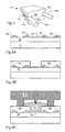
- FIG. 1 represents a perspective view of a chip element 10 secured to two parallel wires 12 a and 12 b, as described in Patent application WO2009112644.
- Element 10 is of general parallelepipedic shape and two of its opposite side surfaces are provided with respective parallel grooves 14 a and 14 b which extend over the whole length of element 10 . Each of these grooves respectively receives one of wires 12 a and 12 b.
- Wires 12 a and 12 b generally have a role of electric connection, for example to supply electric current to a light-emitting diode formed in the chip of element 10 .
- Wires 12 a and 12 b are thus conducting and are in electric connection with the chip by means of a conducting bump 16 formed on the side wall of each groove.
- the width of the grooves and the height of bumps 16 are selected according to the diameter of wires 12 so that each wire is pinched between the bump and the opposite side wall of groove 14 .
- An element of the type of FIG. 1 is generally made up of two parts.
- a first part 18 a corresponding to the bottom third of the element, is formed by the chip.
- a second part 18 b corresponding to the remaining top part of the element, forms a protective cover.
- the active surface of the chip, facing cover 18 b, comprises bumps 16 and forms a first side wall of grooves 14 .
- Cover 18 b has a T-shaped cross-section so that it is able to form the second side wall and the bottom of the grooves.
- a fabrication method is therefore provided to fabricate chip elements ( 10 ) provided with a groove ( 14 ) from devices ( 22 ) formed on a wafer ( 20 ).
- the method comprises the steps consisting in depositing a sacrificial film ( 26 ) on wafer ( 20 ) so as to leave a central part of each device ( 22 ) exposed and to cover an edge of the device at the level of which the groove is to be formed; applying a mold ( 28 ) on the sacrificial film; injecting a hardenable material ( 30 ) into the mold; hardening the hardenable material; dicing the wafer between the devices; and eliminating the sacrificial film.
- FIG. 1 represents a perspective view of a chip element secured to two wires
- FIGS. 2A to 2F represent various steps of a method whereby chip elements with grooves of precise and reproducible width can be fabricated.
- FIG. 2A represents a partial cross-sectional view of a wafer 20 on which a set of integrated devices 22 has been formed corresponding to chips 18 a of the chip elements to be achieved. Each of these devices 22 is provided, on two of the edges thereof, with conducting bumps 16 subsequently serving the purpose of establishing contact with wires 12 .
- Wafer 20 for example made from silicon, has in this example been thinned so that the thickness of the latter is compatible with the required dimensions of the final chip elements.
- the latter has been secured via its rear surface to a support plate, or “handle” 24 , giving the assembly the required rigidity for the various steps of the fabrication method. Assembly of the wafer 20 on support plate 24 must as a general rule withstand the high temperatures encountered during the various fabrication operations of devices 22 .
- a sacrificial film 26 is deposited in a thick layer, for example 100 ⁇ m, on the top surface of wafer 20 .
- This film 26 is made from a material able to be patterned, planarized, and eliminated by usual techniques in the semiconductors field.
- the material is for example a resin, a polyimide, or a metal.
- the thickness of this film 26 defines the width of future grooves 14 .
- the usual deposition techniques enable an amply sufficient precision of the thickness of the film to be obtained.
- the distance that is required to be precise is in fact that separating the top of each bump 16 from the opposite wall of the groove.
- the techniques for fabricating bumps 16 also enable the required precision to be obtained.
- film 26 is patterned, for example by photolithography, to leave the central parts of devices 22 exposed, while covering the edges provided with bumps 16 (the areas designed t o formed the first side walls o f the future grooves). Patterning is preferably anisotropic so that the openings in film 26 present walls perpendicular to the wafer, these walls defining the bottoms of the future grooves.
- a mold 28 comprising cavities in correspondence with devices 22 is applied on film 26 .
- the cavities of mold 28 together with the holes in film 26 , define the shape of the future covers 18 b of the chip elements, for example covers with a T-shaped cross-section.
- a hardenable liquid 30 presenting the desired properties for the covers for example a transparent epoxy resin in the case where devices 22 are light-emitting diodes, is injected into each cavity of mold 28 .
- FIG. 2D represents the result obtained after resin 30 has hardened and mold 28 has been removed. Resin 30 , overlying devices 22 , forms covers 18 b and leaves film 26 exposed in areas surrounding devices 22 .
- dicing is performed via the top surface to separate devices 22 and form chips 18 a.
- the dicing cuts 32 pass in the spaces left by the mold between covers 18 b, pass through film 26 , and start to cut wafer 20 without passing through the latter.
- Elimination of sacrificial film 26 is preferably performed after dicing. By proceeding in this order, the dicing shavings are prevented from depositing in grooves 14 and from hindering establishment of the subsequent electric contact between wires 12 and bumps 16 .
- Removal of support plate 24 is then performed, followed by grinding of wafer 20 on the rear surface up to a plane P at the level of the bottoms of the dicing cuts to obtain individual chip elements 10 .
- covers 18 b can for example by pressed on a removable adhesive support, not shown. After grinding, individual chip elements 10 remain stuck to the adhesive support and are then in a conditioning similar to that of conventional chips after wafer dicing. The chip elements can then be exploited by conventional chip-handling tools.
- support plate 24 is removed before the dicing step of FIG. 2E and wafer 20 is secured via its rear surface to a removable adhesive support. Dicing cuts 32 then pass through wafer 20 and cut into the adhesive support.
- One advantage of this variant is that it avoids the grinding step of the rear surface of wafer 20 and a risk of the shavings due to grinding depositing in grooves 14 .
- the mold illustrated in FIG. 2C does not comprise an individualized cavity for each device 22 , but a single cavity extending over the whole set of devices 22 .
- the mold illustrated in FIG. 2C does not comprise an individualized cavity for each device 22 , but a single cavity extending over the whole set of devices 22 .
- Individual covers 18 b are then formed in the step of FIG. 2E by dicing cuts 32 .
Landscapes
- Dicing (AREA)
- Encapsulation Of And Coatings For Semiconductor Or Solid State Devices (AREA)
- Micromachines (AREA)
Abstract
Description
Claims (5)
Applications Claiming Priority (2)
| Application Number | Priority Date | Filing Date | Title |
|---|---|---|---|
| FR1002080 | 2010-05-18 | ||
| FR1002080A FR2960339B1 (en) | 2010-05-18 | 2010-05-18 | METHOD FOR PRODUCING CHIP ELEMENTS WITH WIRE INSERTION GROOVES |
Publications (2)
| Publication Number | Publication Date |
|---|---|
| US20110287606A1 US20110287606A1 (en) | 2011-11-24 |
| US8258044B2 true US8258044B2 (en) | 2012-09-04 |
Family
ID=43430883
Family Applications (1)
| Application Number | Title | Priority Date | Filing Date |
|---|---|---|---|
| US13/103,533 Expired - Fee Related US8258044B2 (en) | 2010-05-18 | 2011-05-09 | Method for fabricating chip elements provided with wire insertion grooves |
Country Status (5)
| Country | Link |
|---|---|
| US (1) | US8258044B2 (en) |
| EP (1) | EP2388806B1 (en) |
| JP (1) | JP5829047B2 (en) |
| CN (1) | CN102254868B (en) |
| FR (1) | FR2960339B1 (en) |
Cited By (26)
| Publication number | Priority date | Publication date | Assignee | Title |
|---|---|---|---|---|
| US20110198735A1 (en) * | 2008-10-21 | 2011-08-18 | Commissariat A L'energie Atomique Et Aux Energies Alternatives | Assembly of a microelectronic chip having a groove with a wire element in the form of a strand, and method for assembly |
| US9888573B2 (en) | 2012-09-17 | 2018-02-06 | Commissariat A L'energie Atomique Et Aux Energies Alternatives | Cap for a chip device having a groove, device provided with said cap, assembly consisting of the device and a wire element, and manufacturing method thereof |
| US10431648B2 (en) | 2014-05-02 | 2019-10-01 | Invensas Corporation | Making electrical components in handle wafers of integrated circuit packages |
| US11201265B2 (en) | 2018-09-27 | 2021-12-14 | Lumileds Llc | Micro light emitting devices |
| US11569415B2 (en) | 2020-03-11 | 2023-01-31 | Lumileds Llc | Light emitting diode devices with defined hard mask opening |
| US11600656B2 (en) | 2020-12-14 | 2023-03-07 | Lumileds Llc | Light emitting diode device |
| US11626538B2 (en) | 2020-10-29 | 2023-04-11 | Lumileds Llc | Light emitting diode device with tunable emission |
| US11705534B2 (en) | 2020-12-01 | 2023-07-18 | Lumileds Llc | Methods of making flip chip micro light emitting diodes |
| US11735695B2 (en) | 2020-03-11 | 2023-08-22 | Lumileds Llc | Light emitting diode devices with current spreading layer |
| US11777059B2 (en) | 2019-11-20 | 2023-10-03 | Lumileds Llc | Pixelated light-emitting diode for self-aligned photoresist patterning |
| US11848402B2 (en) | 2020-03-11 | 2023-12-19 | Lumileds Llc | Light emitting diode devices with multilayer composite film including current spreading layer |
| US11901491B2 (en) | 2020-10-29 | 2024-02-13 | Lumileds Llc | Light emitting diode devices |
| US11935987B2 (en) | 2021-11-03 | 2024-03-19 | Lumileds Llc | Light emitting diode arrays with a light-emitting pixel area |
| US11942507B2 (en) | 2020-03-11 | 2024-03-26 | Lumileds Llc | Light emitting diode devices |
| US11955583B2 (en) | 2020-12-01 | 2024-04-09 | Lumileds Llc | Flip chip micro light emitting diodes |
| US11961875B2 (en) | 2017-12-20 | 2024-04-16 | Lumileds Llc | Monolithic segmented LED array architecture with islanded epitaxial growth |
| US12040432B2 (en) | 2020-10-30 | 2024-07-16 | Lumileds Llc | Light emitting diode devices with patterned TCO layer including different thicknesses |
| US12402440B2 (en) | 2021-09-03 | 2025-08-26 | Lumileds Llc | Light emitting diode devices with bonding and/or ohmic contact-reflective material |
| US12419137B2 (en) | 2021-09-10 | 2025-09-16 | Lumileds Llc | Light emitting diodes with segmented anodes by pixel |
| US12431478B2 (en) | 2021-09-29 | 2025-09-30 | Lumileds Singapore Pte. Ltd. | Hybrid CMOS micro-LED display layout |
| US12433080B2 (en) | 2021-09-29 | 2025-09-30 | Lumileds Singapore Pte. Ltd. | Hybrid CMOS micro-LED display layout |
| US12484346B2 (en) | 2021-09-03 | 2025-11-25 | Lumileds Singapore Pte. Ltd. | Light emitting diode devices with bonding and/or ohmic contact-reflective material |
| US12490570B2 (en) | 2021-11-12 | 2025-12-02 | Lumileds Singapore Pte. Ltd. | Thin-film LED array with low refractive index patterned structures |
| US12532594B2 (en) | 2017-12-20 | 2026-01-20 | Adeia Semiconductor Inc. | Monolithic segmented LED array architecture with islanded epitaxial growth |
| US12568728B2 (en) | 2021-09-29 | 2026-03-03 | Lumileds Singapore Pte. Ltd. | Hybrid CMOS micro-LED display layout |
| US12588326B2 (en) | 2022-11-07 | 2026-03-24 | Lumileds Singapore Pte. Ltd. | Composite cathode contact for monolithically integrated micro-LEDs, mini-LEDs and LED arrays |
Families Citing this family (10)
| Publication number | Priority date | Publication date | Assignee | Title |
|---|---|---|---|---|
| FR2928491A1 (en) * | 2008-03-06 | 2009-09-11 | Commissariat Energie Atomique | METHOD AND DEVICE FOR MANUFACTURING AN ASSEMBLY OF AT LEAST TWO MICROELECTRONIC CHIPS |
| NL2011512C2 (en) | 2013-09-26 | 2015-03-30 | Besi Netherlands B V | Method for moulding and surface processing electronic components and electronic component produced with this method. |
| US9355997B2 (en) | 2014-03-12 | 2016-05-31 | Invensas Corporation | Integrated circuit assemblies with reinforcement frames, and methods of manufacture |
| US20150262902A1 (en) | 2014-03-12 | 2015-09-17 | Invensas Corporation | Integrated circuits protected by substrates with cavities, and methods of manufacture |
| US9741649B2 (en) | 2014-06-04 | 2017-08-22 | Invensas Corporation | Integrated interposer solutions for 2D and 3D IC packaging |
| US9412806B2 (en) | 2014-06-13 | 2016-08-09 | Invensas Corporation | Making multilayer 3D capacitors using arrays of upstanding rods or ridges |
| US9252127B1 (en) | 2014-07-10 | 2016-02-02 | Invensas Corporation | Microelectronic assemblies with integrated circuits and interposers with cavities, and methods of manufacture |
| US9478504B1 (en) | 2015-06-19 | 2016-10-25 | Invensas Corporation | Microelectronic assemblies with cavities, and methods of fabrication |
| FR3053157B1 (en) | 2016-06-22 | 2018-10-12 | Commissariat A L'energie Atomique Et Aux Energies Alternatives | MICROELECTRONIC DEVICE HOUSING |
| FR3065578B1 (en) * | 2017-04-19 | 2019-05-03 | Primo1D | METHOD FOR ASSEMBLING A MICROELECTRONIC CHIP ON A WIRED ELEMENT |
Citations (10)
| Publication number | Priority date | Publication date | Assignee | Title |
|---|---|---|---|---|
| EP0360660A1 (en) | 1988-09-23 | 1990-03-28 | Valeo Vision | Light-emitting diode array |
| US5501784A (en) * | 1993-03-12 | 1996-03-26 | Microparts Gmbh | Process for producing microstructure metallic elements |
| US20030162324A1 (en) | 2002-02-25 | 2003-08-28 | Seiko Epson Corporation | Semiconductor wafer with spacer and its manufacturing method, semiconductor device and its manufacturing method, and circuit substrate and electronic device |
| US20050223552A1 (en) | 2004-04-08 | 2005-10-13 | Neal Meyer | Bonding an interconnect to a circuit device and related devices |
| US7160429B2 (en) * | 2002-05-07 | 2007-01-09 | Microfabrica Inc. | Electrochemically fabricated hermetically sealed microstructures and methods of and apparatus for producing such structures |
| US7229542B2 (en) * | 2002-05-07 | 2007-06-12 | Microfabrica Inc. | Methods of and apparatus for molding structures using sacrificial metal patterns |
| US20070178666A1 (en) | 2006-01-31 | 2007-08-02 | Stats Chippac Ltd. | Integrated circuit system with waferscale spacer system |
| US7252861B2 (en) * | 2002-05-07 | 2007-08-07 | Microfabrica Inc. | Methods of and apparatus for electrochemically fabricating structures via interlaced layers or via selective etching and filling of voids |
| EP2099060A1 (en) | 2008-03-06 | 2009-09-09 | Commissariat à l'Energie Atomique | Method and device for manufacturing an assembly with at least two microelectronic chips |
| FR2937464A1 (en) | 2008-10-21 | 2010-04-23 | Commissariat Energie Atomique | ASSEMBLY OF A GROOVED MICROELECTRONIC CHIP WITH A TORON-WIRED ELEMENT AND METHOD OF ASSEMBLY |
Family Cites Families (7)
| Publication number | Priority date | Publication date | Assignee | Title |
|---|---|---|---|---|
| JPH07256763A (en) * | 1994-03-24 | 1995-10-09 | Olympus Optical Co Ltd | Manufacture of structural body, manufacturing device and structural body manufactured by that method |
| JP3832353B2 (en) * | 2002-02-15 | 2006-10-11 | 松下電器産業株式会社 | Manufacturing method of semiconductor device |
| US6805433B1 (en) * | 2003-05-19 | 2004-10-19 | Xerox Corporation | Integrated side shooter inkjet architecture with round nozzles |
| JP5024047B2 (en) * | 2005-10-07 | 2012-09-12 | 株式会社ニコン | Manufacturing method of microstructure |
| TWI313501B (en) * | 2006-03-22 | 2009-08-11 | Ind Tech Res Inst | A process for manufacture plastic package of mems devices and the structure for the same |
| US20080079150A1 (en) * | 2006-09-28 | 2008-04-03 | Juergen Simon | Die arrangement and method for producing a die arrangement |
| JP4538764B2 (en) * | 2008-07-24 | 2010-09-08 | カシオ計算機株式会社 | Semiconductor device and manufacturing method thereof |
-
2010
- 2010-05-18 FR FR1002080A patent/FR2960339B1/en not_active Expired - Fee Related
-
2011
- 2011-05-05 EP EP11354017.3A patent/EP2388806B1/en not_active Not-in-force
- 2011-05-09 US US13/103,533 patent/US8258044B2/en not_active Expired - Fee Related
- 2011-05-17 JP JP2011110054A patent/JP5829047B2/en not_active Expired - Fee Related
- 2011-05-18 CN CN201110132957.8A patent/CN102254868B/en not_active Expired - Fee Related
Patent Citations (14)
| Publication number | Priority date | Publication date | Assignee | Title |
|---|---|---|---|---|
| EP0360660A1 (en) | 1988-09-23 | 1990-03-28 | Valeo Vision | Light-emitting diode array |
| US4990971A (en) | 1988-09-23 | 1991-02-05 | Valeo Vision | Light emiting diode network |
| US5501784A (en) * | 1993-03-12 | 1996-03-26 | Microparts Gmbh | Process for producing microstructure metallic elements |
| US20030162324A1 (en) | 2002-02-25 | 2003-08-28 | Seiko Epson Corporation | Semiconductor wafer with spacer and its manufacturing method, semiconductor device and its manufacturing method, and circuit substrate and electronic device |
| US7229542B2 (en) * | 2002-05-07 | 2007-06-12 | Microfabrica Inc. | Methods of and apparatus for molding structures using sacrificial metal patterns |
| US7160429B2 (en) * | 2002-05-07 | 2007-01-09 | Microfabrica Inc. | Electrochemically fabricated hermetically sealed microstructures and methods of and apparatus for producing such structures |
| US7252861B2 (en) * | 2002-05-07 | 2007-08-07 | Microfabrica Inc. | Methods of and apparatus for electrochemically fabricating structures via interlaced layers or via selective etching and filling of voids |
| US20050223552A1 (en) | 2004-04-08 | 2005-10-13 | Neal Meyer | Bonding an interconnect to a circuit device and related devices |
| US20070178666A1 (en) | 2006-01-31 | 2007-08-02 | Stats Chippac Ltd. | Integrated circuit system with waferscale spacer system |
| EP2099060A1 (en) | 2008-03-06 | 2009-09-09 | Commissariat à l'Energie Atomique | Method and device for manufacturing an assembly with at least two microelectronic chips |
| US20090227069A1 (en) | 2008-03-06 | 2009-09-10 | Commissariat A L'energie Atomique | Method and device for fabricating an assembly of at least two microelectronic chips |
| WO2009112644A1 (en) | 2008-03-06 | 2009-09-17 | Commissariat A L'energie Atomique | Assembly including a wire member and a microelectronic chip with a notch, including at least one stud for holding the wire member |
| US20110001237A1 (en) | 2008-03-06 | 2011-01-06 | Commissariat A L'energie Atomique Et Aux Energies Alternatives | Assembly of a wire element with a microelectronic chip with a groove comprising at least one bump securing the wire element |
| FR2937464A1 (en) | 2008-10-21 | 2010-04-23 | Commissariat Energie Atomique | ASSEMBLY OF A GROOVED MICROELECTRONIC CHIP WITH A TORON-WIRED ELEMENT AND METHOD OF ASSEMBLY |
Cited By (33)
| Publication number | Priority date | Publication date | Assignee | Title |
|---|---|---|---|---|
| US8611101B2 (en) * | 2008-10-21 | 2013-12-17 | Commissariat A L'energie Atomique Et Aux Energies Alternatives | Assembly of a microelectronic chip having a groove with a wire element in the form of a strand, and method for assembly |
| US20110198735A1 (en) * | 2008-10-21 | 2011-08-18 | Commissariat A L'energie Atomique Et Aux Energies Alternatives | Assembly of a microelectronic chip having a groove with a wire element in the form of a strand, and method for assembly |
| US9888573B2 (en) | 2012-09-17 | 2018-02-06 | Commissariat A L'energie Atomique Et Aux Energies Alternatives | Cap for a chip device having a groove, device provided with said cap, assembly consisting of the device and a wire element, and manufacturing method thereof |
| US10431648B2 (en) | 2014-05-02 | 2019-10-01 | Invensas Corporation | Making electrical components in handle wafers of integrated circuit packages |
| US12532594B2 (en) | 2017-12-20 | 2026-01-20 | Adeia Semiconductor Inc. | Monolithic segmented LED array architecture with islanded epitaxial growth |
| US11961875B2 (en) | 2017-12-20 | 2024-04-16 | Lumileds Llc | Monolithic segmented LED array architecture with islanded epitaxial growth |
| US11735691B2 (en) | 2018-09-27 | 2023-08-22 | Lumileds Llc | Micro light emitting devices |
| US11201265B2 (en) | 2018-09-27 | 2021-12-14 | Lumileds Llc | Micro light emitting devices |
| US11271033B2 (en) | 2018-09-27 | 2022-03-08 | Lumileds Llc | Micro light emitting devices |
| US11777059B2 (en) | 2019-11-20 | 2023-10-03 | Lumileds Llc | Pixelated light-emitting diode for self-aligned photoresist patterning |
| US11569415B2 (en) | 2020-03-11 | 2023-01-31 | Lumileds Llc | Light emitting diode devices with defined hard mask opening |
| US11735695B2 (en) | 2020-03-11 | 2023-08-22 | Lumileds Llc | Light emitting diode devices with current spreading layer |
| US11942507B2 (en) | 2020-03-11 | 2024-03-26 | Lumileds Llc | Light emitting diode devices |
| US11848402B2 (en) | 2020-03-11 | 2023-12-19 | Lumileds Llc | Light emitting diode devices with multilayer composite film including current spreading layer |
| US11784286B2 (en) | 2020-03-11 | 2023-10-10 | Lumileds Llc | Light emitting diode devices with defined hard mask opening |
| US11901491B2 (en) | 2020-10-29 | 2024-02-13 | Lumileds Llc | Light emitting diode devices |
| US11777061B2 (en) | 2020-10-29 | 2023-10-03 | Lumileds Llc | Light emitting diode device with tunable emission |
| US11626538B2 (en) | 2020-10-29 | 2023-04-11 | Lumileds Llc | Light emitting diode device with tunable emission |
| US12040432B2 (en) | 2020-10-30 | 2024-07-16 | Lumileds Llc | Light emitting diode devices with patterned TCO layer including different thicknesses |
| US11705534B2 (en) | 2020-12-01 | 2023-07-18 | Lumileds Llc | Methods of making flip chip micro light emitting diodes |
| US11955583B2 (en) | 2020-12-01 | 2024-04-09 | Lumileds Llc | Flip chip micro light emitting diodes |
| US12040423B2 (en) | 2020-12-01 | 2024-07-16 | Lumileds Llc | Methods of making flip chip micro light emitting diodes |
| US11923402B2 (en) | 2020-12-14 | 2024-03-05 | Lumileds Llc | Light emitting diode device |
| US11600656B2 (en) | 2020-12-14 | 2023-03-07 | Lumileds Llc | Light emitting diode device |
| US12402440B2 (en) | 2021-09-03 | 2025-08-26 | Lumileds Llc | Light emitting diode devices with bonding and/or ohmic contact-reflective material |
| US12484346B2 (en) | 2021-09-03 | 2025-11-25 | Lumileds Singapore Pte. Ltd. | Light emitting diode devices with bonding and/or ohmic contact-reflective material |
| US12419137B2 (en) | 2021-09-10 | 2025-09-16 | Lumileds Llc | Light emitting diodes with segmented anodes by pixel |
| US12431478B2 (en) | 2021-09-29 | 2025-09-30 | Lumileds Singapore Pte. Ltd. | Hybrid CMOS micro-LED display layout |
| US12433080B2 (en) | 2021-09-29 | 2025-09-30 | Lumileds Singapore Pte. Ltd. | Hybrid CMOS micro-LED display layout |
| US12568728B2 (en) | 2021-09-29 | 2026-03-03 | Lumileds Singapore Pte. Ltd. | Hybrid CMOS micro-LED display layout |
| US11935987B2 (en) | 2021-11-03 | 2024-03-19 | Lumileds Llc | Light emitting diode arrays with a light-emitting pixel area |
| US12490570B2 (en) | 2021-11-12 | 2025-12-02 | Lumileds Singapore Pte. Ltd. | Thin-film LED array with low refractive index patterned structures |
| US12588326B2 (en) | 2022-11-07 | 2026-03-24 | Lumileds Singapore Pte. Ltd. | Composite cathode contact for monolithically integrated micro-LEDs, mini-LEDs and LED arrays |
Also Published As
| Publication number | Publication date |
|---|---|
| US20110287606A1 (en) | 2011-11-24 |
| CN102254868B (en) | 2016-07-06 |
| FR2960339A1 (en) | 2011-11-25 |
| EP2388806A1 (en) | 2011-11-23 |
| EP2388806B1 (en) | 2018-12-19 |
| JP2011240481A (en) | 2011-12-01 |
| JP5829047B2 (en) | 2015-12-09 |
| FR2960339B1 (en) | 2012-05-18 |
| CN102254868A (en) | 2011-11-23 |
Similar Documents
| Publication | Publication Date | Title |
|---|---|---|
| US8258044B2 (en) | Method for fabricating chip elements provided with wire insertion grooves | |
| US11302579B2 (en) | Composite wafer, semiconductor device and electronic component | |
| JP5637333B1 (en) | Semiconductor piece manufacturing method, circuit board and electronic device including semiconductor piece, and substrate dicing method | |
| US8072044B2 (en) | Semiconductor die containing lateral edge shapes and textures | |
| US10923460B2 (en) | Device and methods for the transfer of chips from a source substrate onto a destination substrate | |
| CN109411369B (en) | Semiconductor package and method of forming same | |
| US20090061595A1 (en) | Method for dividing a semiconductor substrate and a method for producing a semiconductor circuit arrangement | |
| CN103972170B (en) | Semiconductor devices and its production method | |
| CN114730716A (en) | Method for manufacturing functional chip suitable for assembling to wire element | |
| US20250149449A1 (en) | Thinned semiconductor package and related methods | |
| US8058736B2 (en) | Semiconductor device having heat spreader with center opening | |
| US7179720B2 (en) | Pre-fabrication scribing | |
| JP5115295B2 (en) | Semiconductor device and manufacturing method thereof | |
| JP2008235723A (en) | Wafer structure and manufacturing method thereof | |
| JP2004349550A (en) | Semiconductor device and manufacturing method thereof | |
| JP4589536B2 (en) | Method for manufacturing thermoelectric element | |
| JP4507889B2 (en) | Manufacturing method of semiconductor device | |
| CN103871974B (en) | Semiconductor device and production method thereof | |
| CN103871974A (en) | Semiconductor Device and Method of Producing the Same | |
| CN107154360A (en) | Optical electronic device and its manufacture method |
Legal Events
| Date | Code | Title | Description |
|---|---|---|---|
| AS | Assignment |
Owner name: COMMISSARIAT A L'ENERGIE ATOMIQUE ET AUX ENERGIES Free format text: ASSIGNMENT OF ASSIGNORS INTEREST;ASSIGNORS:BRUN, JEAN;VICARD, DOMINIQUE;REEL/FRAME:026256/0508 Effective date: 20110414 |
|
| STCF | Information on status: patent grant |
Free format text: PATENTED CASE |
|
| FPAY | Fee payment |
Year of fee payment: 4 |
|
| AS | Assignment |
Owner name: CONTECH ENGINEERED SOLUTIONS, LLC, GEORGIA Free format text: RELEASE BY SECURED PARTY;ASSIGNOR:WELLS FARGO CAPITAL FINANCE, LLC;REEL/FRAME:040797/0343 Effective date: 20161115 |
|
| FEPP | Fee payment procedure |
Free format text: MAINTENANCE FEE REMINDER MAILED (ORIGINAL EVENT CODE: REM.); ENTITY STATUS OF PATENT OWNER: LARGE ENTITY |
|
| LAPS | Lapse for failure to pay maintenance fees |
Free format text: PATENT EXPIRED FOR FAILURE TO PAY MAINTENANCE FEES (ORIGINAL EVENT CODE: EXP.); ENTITY STATUS OF PATENT OWNER: LARGE ENTITY |
|
| STCH | Information on status: patent discontinuation |
Free format text: PATENT EXPIRED DUE TO NONPAYMENT OF MAINTENANCE FEES UNDER 37 CFR 1.362 |
|
| FP | Lapsed due to failure to pay maintenance fee |
Effective date: 20200904 |