US8217722B2 - Power amplifier - Google Patents
Power amplifier Download PDFInfo
- Publication number
- US8217722B2 US8217722B2 US13/079,046 US201113079046A US8217722B2 US 8217722 B2 US8217722 B2 US 8217722B2 US 201113079046 A US201113079046 A US 201113079046A US 8217722 B2 US8217722 B2 US 8217722B2
- Authority
- US
- United States
- Prior art keywords
- fet
- transistor
- voltage
- electrode
- gate electrode
- Prior art date
- Legal status (The legal status is an assumption and is not a legal conclusion. Google has not performed a legal analysis and makes no representation as to the accuracy of the status listed.)
- Active
Links
Images


Classifications
-
- H—ELECTRICITY
- H03—ELECTRONIC CIRCUITRY
- H03F—AMPLIFIERS
- H03F1/00—Details of amplifiers with only discharge tubes, only semiconductor devices or only unspecified devices as amplifying elements
- H03F1/30—Modifications of amplifiers to reduce influence of variations of temperature or supply voltage or other physical parameters
-
- H—ELECTRICITY
- H03—ELECTRONIC CIRCUITRY
- H03F—AMPLIFIERS
- H03F3/00—Amplifiers with only discharge tubes or only semiconductor devices as amplifying elements
- H03F3/189—High-frequency amplifiers, e.g. radio frequency amplifiers
- H03F3/19—High-frequency amplifiers, e.g. radio frequency amplifiers with semiconductor devices only
- H03F3/195—High-frequency amplifiers, e.g. radio frequency amplifiers with semiconductor devices only in integrated circuits
-
- H—ELECTRICITY
- H03—ELECTRONIC CIRCUITRY
- H03F—AMPLIFIERS
- H03F1/00—Details of amplifiers with only discharge tubes, only semiconductor devices or only unspecified devices as amplifying elements
- H03F1/02—Modifications of amplifiers to raise the efficiency, e.g. gliding Class A stages, use of an auxiliary oscillation
- H03F1/0205—Modifications of amplifiers to raise the efficiency, e.g. gliding Class A stages, use of an auxiliary oscillation in transistor amplifiers
- H03F1/0277—Selecting one or more amplifiers from a plurality of amplifiers
-
- H—ELECTRICITY
- H03—ELECTRONIC CIRCUITRY
- H03F—AMPLIFIERS
- H03F3/00—Amplifiers with only discharge tubes or only semiconductor devices as amplifying elements
- H03F3/189—High-frequency amplifiers, e.g. radio frequency amplifiers
-
- H—ELECTRICITY
- H03—ELECTRONIC CIRCUITRY
- H03F—AMPLIFIERS
- H03F3/00—Amplifiers with only discharge tubes or only semiconductor devices as amplifying elements
- H03F3/20—Power amplifiers, e.g. Class B amplifiers, Class C amplifiers
-
- H—ELECTRICITY
- H03—ELECTRONIC CIRCUITRY
- H03F—AMPLIFIERS
- H03F3/00—Amplifiers with only discharge tubes or only semiconductor devices as amplifying elements
- H03F3/20—Power amplifiers, e.g. Class B amplifiers, Class C amplifiers
- H03F3/24—Power amplifiers, e.g. Class B amplifiers, Class C amplifiers of transmitter output stages
- H03F3/245—Power amplifiers, e.g. Class B amplifiers, Class C amplifiers of transmitter output stages with semiconductor devices only
-
- H—ELECTRICITY
- H03—ELECTRONIC CIRCUITRY
- H03F—AMPLIFIERS
- H03F3/00—Amplifiers with only discharge tubes or only semiconductor devices as amplifying elements
- H03F3/72—Gated amplifiers, i.e. amplifiers which are rendered operative or inoperative by means of a control signal
-
- H—ELECTRICITY
- H03—ELECTRONIC CIRCUITRY
- H03G—CONTROL OF AMPLIFICATION
- H03G1/00—Details of arrangements for controlling amplification
- H03G1/0005—Circuits characterised by the type of controlling devices operated by a controlling current or voltage signal
- H03G1/0088—Circuits characterised by the type of controlling devices operated by a controlling current or voltage signal using discontinuously variable devices, e.g. switch-operated
-
- H—ELECTRICITY
- H03—ELECTRONIC CIRCUITRY
- H03F—AMPLIFIERS
- H03F2200/00—Indexing scheme relating to amplifiers
- H03F2200/27—A biasing circuit node being switched in an amplifier circuit
-
- H—ELECTRICITY
- H03—ELECTRONIC CIRCUITRY
- H03F—AMPLIFIERS
- H03F2200/00—Indexing scheme relating to amplifiers
- H03F2200/411—Indexing scheme relating to amplifiers the output amplifying stage of an amplifier comprising two power stages
-
- H—ELECTRICITY
- H03—ELECTRONIC CIRCUITRY
- H03F—AMPLIFIERS
- H03F2203/00—Indexing scheme relating to amplifiers with only discharge tubes or only semiconductor devices as amplifying elements covered by H03F3/00
- H03F2203/72—Indexing scheme relating to gated amplifiers, i.e. amplifiers which are rendered operative or inoperative by means of a control signal
- H03F2203/7206—Indexing scheme relating to gated amplifiers, i.e. amplifiers which are rendered operative or inoperative by means of a control signal the gated amplifier being switched on or off by a switch in the bias circuit of the amplifier controlling a bias voltage in the amplifier
-
- H—ELECTRICITY
- H03—ELECTRONIC CIRCUITRY
- H03F—AMPLIFIERS
- H03F2203/00—Indexing scheme relating to amplifiers with only discharge tubes or only semiconductor devices as amplifying elements covered by H03F3/00
- H03F2203/72—Indexing scheme relating to gated amplifiers, i.e. amplifiers which are rendered operative or inoperative by means of a control signal
- H03F2203/7236—Indexing scheme relating to gated amplifiers, i.e. amplifiers which are rendered operative or inoperative by means of a control signal the gated amplifier being switched on or off by putting into parallel or not, by choosing between amplifiers by (a ) switch(es)
Definitions
- the present invention relates to a power amplifier formed using a BiFET process. More specifically, the present invention relates to a power amplifier capable of suppressing leakage current without increasing chip areas and manufacturing costs.
- GaAs-FET field-effect transistor
- a GaAs-HBT hetero junction bipolar transistor
- a GaAs-HBT power amplifier does not require negative gate bias voltage, enables single power source operation, and has more even bias characteristics than the FET type. In recent years, therefore, a GaAs-HBT power amplifier has been actively used in mobile telephones such as CDMA or wireless LANs.
- a reference voltage generating circuit wherein the gain variation due to process variation is suppressed, has been proposed (for example, refer to FIG. 1 in Japanese Patent Application Laid-Open No. 2010-124408). Furthermore, a reference voltage generating circuit, wherein the ON voltage of the enable voltage using a depletion mode FET has also been proposed (for example, refer to FIG. 3 in Japanese Patent Application Laid-Open No. 2010-124408).
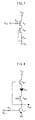
- FIG. 44 is a diagram showing the relation between the enable voltage and the leakage current of a power amplifier according to the first reference example.
- the power amplifier is formed by applying the circuit in FIG. 3 of Japanese Patent Application Laid-Open No. 2010-124408 to the reference voltage generating circuit of the power amplifier circuit in FIG. 12 of Japanese Patent Application Laid-Open No. 2010-124408.
- the first reference example operates with a low enable voltage (higher than 1.3 V) by using a low enable voltage type reference voltage generating circuit.
- FIG. 45 is a diagram showing the relation between the enable voltage and the leakage current of a power amplifier according to the second reference example.
- the power amplifier is formed by applying the circuit in FIG. 1 of Japanese Patent Application Laid-Open No. 2010-124408 to the reference voltage generating circuit of the power amplifier circuit in FIG. 12 of Japanese Patent Application Laid-Open No. 2010-124408, and forming a two-step inverter in the front stage of the reference voltage generating circuit. Since the reference voltage generating circuit according to the second reference example corresponds to the enable voltage higher than 2.1 V, the second reference example can be operated with an elevated low enable voltage (higher than 1.3 V) by the inverter.
- the current capacity of an enable terminal is 0.1 mA or less; that the power amplifier is turned OFF (shutdown) when the enable voltage is Low (0 to 0.5 V); and that the power amplifier is turned ON when the enable voltage is High (higher than 1.3 V) and the bias current flows to be an amplification enable state.
- the leakage current when the enable voltage is 0 V is good
- the leakage current when the enable voltage is 0.5 V becomes larger than in the example shown in FIG. 45 . Therefore, if the operation current of an inverter having no shutdown functions is 10 ⁇ A and the leakage current of other blocks is sufficiently low, the second reference example is suitable for satisfying the specifications of the enable voltage. In particular, even when the enable voltage is 0.5 V, the leakage current specification for the normally required entire power amplifier at the time of shutdown (lower than 10 ⁇ A) can be easily satisfied. However, even at the time of shutdown, the reduction of the current consumed by the continuously operating inverter is important.
- the collector load of the transistor if the collector load of the transistor is enlarged, the current can be reduced.
- the threshold voltage of the transistor is about ⁇ 0.8 V, it is required to make the collector load be about 100 k ⁇ to suppress consumed current to several microamperes.
- a thin metal film resistor is normally utilized for a Bi-FET power amplifier for mobile telephones, the sheet resistance thereof is as low as about 30 to 60 ⁇ . Therefore, a significantly large layout area is required for fabricating a thin metal film resistor of 100 k ⁇ , and the chip size expands.
- a metal resistor of k ⁇ order can be utilized, the process step is correspondingly lengthened, and the manufacturing costs elevate.
- an object of the present invention is to provide a power amplifier capable of suppressing leakage current without increasing chip areas and manufacturing costs.
- a power amplifier comprises: an amplifying transistor for amplifying an input signal; a reference voltage generating circuit which generates a reference voltage; a bias circuit generating a bias voltage on the basis of the reference voltage and supplying the bias voltage to the amplifying transistor; and a booster elevating an enable voltage inputted from the exterior and outputting the enable voltage, wherein the reference voltage generating circuit is turned ON/OFF corresponding to an output voltage of the booster, the booster includes: an enable terminal to which the enable voltage is applied; a power source terminal connected to a power source; a transistor having a control electrode connected to the enable terminal, a first electrode connected to the power source terminal, and a second electrode grounded; and a FET resistor connected between the first electrode of the transistor and the power source terminal, wherein a gate electrode of the FET resistor is open.
- the present invention makes it possible to suppress leakage current without increasing chip areas and manufacturing costs.
- FIG. 1 is a block diagram showing a power amplifier according to the first embodiment.
- FIG. 2 is a circuit diagram showing a reference voltage generating circuit according to the first embodiment.
- FIG. 3 is a circuit diagram showing a bias circuit according to the first embodiment.
- FIG. 4 is a circuit diagram showing an inverter according to the first embodiment.
- FIG. 5 is a top view showing a FET resistor according to the first embodiment.
- FIG. 6 is a diagram showing the DC characteristics of the FET resistor according to the first embodiment.
- FIG. 7 is a circuit diagram showing an input circuit according to the first embodiment.
- FIG. 8 is a circuit diagram showing an inverter according to the second embodiment.
- FIG. 9 is a circuit diagram showing an inverter according to the third embodiment.
- FIG. 10 is a diagram showing the DC characteristics of two FET resistors connected in series according to the third embodiment.
- FIG. 11 is a circuit diagram showing an inverter according to the fourth embodiment.
- FIG. 12 is a top view showing a FET resistor according to the fourth embodiment.
- FIG. 13 is a top view showing a FET resistor according to the fifth embodiment.
- FIG. 14 is a top view showing the FET resistor according to the comparative example.
- FIG. 15 is a circuit diagram showing an inverter according to the sixth embodiment.
- FIG. 16 is a circuit diagram showing an inverter according to the seventh embodiment.
- FIG. 17 is a circuit diagram showing an inverter according to the eighth embodiment.
- FIG. 18 is a circuit diagram showing an inverter according to the ninth embodiment.
- FIG. 19 is a top view showing a FET resistor according to the ninth embodiment.
- FIG. 20 is a sectional view showing the FET resistor according to the ninth embodiment.
- FIG. 21 is a diagram showing the DC characteristics of the FET resistor according to the ninth embodiment.
- FIG. 22 is a circuit diagram showing an modified form of the inverter according to the eighth embodiment.
- FIG. 23 is a circuit diagram showing an inverter according to the tenth embodiment.
- FIG. 24 is a diagram showing the relationship between the output voltage and the enable voltage of the inverter according to the tenth embodiment.
- FIG. 25 is a diagram showing the relationship between the current and the enable voltage of the inverter according to the tenth embodiment.
- FIG. 26 is a circuit diagram showing an inverter according to the eleventh embodiment.
- FIG. 27 is a diagram showing the relationship between the output voltage and the enable voltage of the inverter according to the eleventh embodiment.
- FIG. 28 is a diagram showing the relationship between the current of the inverter and the enable voltage according to the eleventh embodiment.
- FIG. 29 is a circuit diagram showing an inverter according to the twelfth embodiment.
- FIG. 30 is a top view showing a FET resistor according to the twelfth embodiment.
- FIG. 31 is a sectional diagram showing the FET resistor according to the twelfth embodiment.
- FIG. 32 is a diagram showing the DC characteristics of the FET resistor according to the twelfth embodiment.
- FIG. 33 is a circuit diagram showing a modified example of the inverter according to the twelfth embodiment.
- FIG. 34 is a circuit diagram showing an inverter according to the thirteenth embodiment.
- FIG. 35 is a circuit diagram showing an inverter according to the fourteenth embodiment.
- FIG. 36 is a circuit diagram showing an inverter according to the fifteenth embodiment.
- FIG. 37 is a circuit, diagram showing a modified example of the inverter according to the fifteenth embodiment.
- FIG. 38 is a block diagram showing a power amplifier according to the sixteenth embodiment.
- FIG. 39 is a circuit diagram showing a reference voltage generating circuit according to the sixteenth embodiment.
- FIG. 40 is a circuit diagram showing a bias circuit according to the sixteenth embodiment.
- FIG. 41 is a diagram showing the relationship between the output voltage and the enable voltage of the reference voltage generating circuit according to the sixteenth embodiment.
- FIG. 42 is a circuit diagram showing a modified example of the reference voltage generating circuit according to the sixteenth embodiment.
- FIG. 43 is a circuit diagram showing a modified example of the bias circuit according to the sixteenth embodiment.
- FIG. 44 is a diagram showing the relation between the enable voltage and the leakage current of a power amplifier according to the first reference example.
- FIG. 45 is a diagram showing the relation between the enable voltage and the leakage current of a power amplifier according to the second reference example.
- FIG. 1 is a block diagram showing a power amplifier according to the first embodiment.
- the power amplifier is formed using a BiFET process for fabricating a FET on the same substrate as the GaAs-HBT, and is equipped with a function for shutdown by an enable voltage inputted from the exterior.
- a first-stage amplifying transistor A 1 and a second-stage amplifying transistor A 2 for amplifying input signals are connected in series.
- a reference voltage generating circuit VG generates a reference voltage.
- a first bias circuit B 1 and a second bias circuit B 2 generate bias voltages on the basis of the reference voltage supplied via a terminal V ref from the reference voltage generating circuit VG, and supply bias voltages to the first-stage amplifying transistor A 1 and the second-stage amplifying transistor A 2 , respectively.
- the gate of a switch F for bypassing the second-stage amplifying transistor A 2 is connected to a control terminal V con via a resistor Rg; the drain thereof is connected to the input side of the second-stage amplifying transistor A 2 via a capacitor Cc 1 ; and the source thereof is connected to the output side of the second-stage amplifying transistor A 2 via a capacitor Cc 2 .
- a resistor Rd is connected between the source and the drain of the switch F.
- An inverter INV elevates the enable voltage inputted from the exterior via an enable terminal V en and outputs it from a terminal V inv .
- the reference voltage generating circuit VG is turned ON/OFF corresponding to the output voltage of the inverter INV.
- the first-stage amplifying transistor A 1 and the second-stage amplifying transistor A 2 are composed of GaAs-HBT.
- FETs are utilized in the first bias circuit B 1 , the second bias circuit B 2 , the reference voltage generating circuit VG, the inverter INV, and the switch F. These are formed on the same GaAs substrate.
- FIG. 2 is a circuit diagram showing a reference voltage generating circuit according to the first embodiment.
- V cb denotes a power source terminal connected to the power source
- V en denotes an enable terminal to which an enable voltage is applied
- V ref denotes a reference voltage terminal to which a reference voltage is applied.
- F dv1 to F dv3 denote depression mode FETs
- Tr v1 to Tr v4 denote HBTs
- R v1 to R v6 denote resistors.
- FIG. 3 is a circuit diagram showing a bias circuit according to the first embodiment.
- V c denotes a power terminal connected to the power source; Tr, and Tr b1 to Tr b5 denote HBTs; R b1 to R b7 denote resistors; and C denotes a capacitor.
- FIG. 4 is a circuit diagram showing an inverter according to the first embodiment. Symbols F di1 and F di2 depression mode FETs, Tr i1 denotes an HBT, and R i1 denotes a resistor. The base of T ri1 is connected to the enable terminal V en via R i1 . The collector of Tr i1 is connected to the power source terminal V cb . The emitter of Tr i1 is grounded. Output signals are outputted from the collector side of Tr i1 via the terminal V inv .
- F di1 and F di2 are connected in series between the collector of Tr i1 and the power source terminal V cb .
- the gate of F di1 is connected to the source of F di2 .
- F di2 is a FET resistor whose gate electrode G is open.
- FIG. 5 is a top view showing a FET resistor according to the first embodiment.
- a source electrode S and a drain electrode D are ohmically connected to the impurity diffused region 10
- a gate electrode G is Schottky connected to the impurity diffused region 10 between them.
- the FET resistor F di2 is a long channel, and the gate width and the gate length thereof are about 3 to 4 ⁇ m and at least 40 ⁇ m, respectively.
- the gate electrode G is not electrically connected to other circuits or wirings, and is kept open.
- FIG. 6 is a diagram showing the DC characteristics of the FET resistor according to the first embodiment.
- the DC characteristics of the FET resistor have a significantly strong nonlinearity and the linear region is as narrow as about ⁇ 0.3V.
- the sheet resistance of the linear region is as high as 700 ⁇ to 1 k ⁇ . Therefore, when the FET resistor is used, a high resistance of about 100 k ⁇ can be realized in a chip area several tens of times smaller than the case where a thin metal film resistor having a sheet resistance of several ohms is used. Since the addition of steps for forming the high sheet metal resistor to the normal BiFET process, the manufacturing costs are not increased.
- a gate open long-channel FET resistor that can be fabricated without adding process steps is used as the resistor of the inverter.
- the leakage current of the entire power amplifier can be suppressed to several ⁇ A or less (about 0.1 ⁇ A to 5 ⁇ A) at a wide Low level of the enable voltage of 0 to 0.8 V without increasing the chip area and manufacturing costs.
- FIG. 7 is a circuit diagram showing an input circuit according to the first embodiment.
- V en ′ denotes a terminal to which the enable voltage is inputted
- F s1 and F s2 denote depression mode FETs
- R s1 and R s2 denote resistors. Since the Tr i1 of the inverter INV is HBT, it is not turned ON without applying the enable voltage higher than 1.4 V to the base. In order to turn it ON by the enable voltage of 0.8 V or higher and 1.4 V or lower, normally the input circuit shown in FIG. 7 is connected to the front stage of the terminal V en of the inverter INV to elevate the enable voltage. This is identical to the inverter INV in other embodiments.
- FIG. 8 is a circuit diagram showing an inverter according to the second embodiment.
- a diode D i1 is added to the inverter in the first embodiment.
- the diode D i1 is connected between F di1 and F di2 .
- the diode D i1 is a Schottky diode formed between the gate and source, and between the gate and drain of a FET, and the ON voltage thereof is about 0.6 to 0.7V.
- the resistance value of F di2 can be reduced by the ON voltage (to about 1 ⁇ 2).
- the threshold voltage of the depletion mode FET is deeper than the ON voltage of the diode D i1 (for example, when the threshold voltage is ⁇ 0.8 V), the circuit is effectively operated.
- the effect in the first embodiment can also be achieved.
- FIG. 9 is a circuit diagram showing an inverter according to the third embodiment.
- a FET resistor F di3 formed by opening the gate of the depletion mode FET is added to the inverter in the second embodiment.
- F di2 and F di3 are connected in series.
- FIG. 10 is a diagram showing the DC characteristics of two FET resistors connected in series according to the third embodiment. Since the range of linear operation is expanded to about 1.2 V, as described above, this embodiment is especially effective when the FET resistor is used in line in a wide voltage range. In addition, the effect in the second embodiment can also be achieved.
- FIG. 11 is a circuit diagram showing an inverter according to the fourth embodiment.
- FIG. 12 is a top view showing a FET resistor according to the fourth embodiment.
- the linear operation range is expanded to about 1.2 V.
- the installation of the source electrode S and the drain electrode D is not required between two gate electrodes G, the size can be reduced compared to the third embodiment.
- the effect in the second embodiment can also be achieved.
- FIG. 13 is a top view showing a FET resistor according to the fifth embodiment.
- Three impurity diffused regions 10 a , 10 b , and 10 c are formed in parallel on a GaAs substrate.
- Gate electrodes G are Schottky-connected to the impurity diffused regions 10 a , 10 b , and 10 c to form three FET resistors. These FET resistors are connected in series.
- the gate electrodes G of the three FET resistors are joined to one another. In the present invention, since the gate electrodes of the FET resistors are opened, the gate electrodes G of the FET resistors can be joined.
- FIG. 14 is a top view showing the FET resistor according to the comparative example.
- the gate electrodes G of three FET resistors are separated. Therefore, the process standard of the distance of the gate electrodes G limits the pattern miniaturization in the time of layout.
- the distance between the gate electrodes G does not limit the pattern miniaturization, and only the distance between the impurity diffused regions limits the pattern miniaturization. Therefore, the layout of the FET resistors can be miniaturized.
- FIG. 15 is a circuit diagram showing an inverter according to the sixth embodiment.
- Tr 1 of the inverter in the sixth embodiment is replaced by F ei1 , which is an enhancement-mode FET, and a Schottky diode D i2 .
- D i2 is connected between the source and the grounding point.
- D i2 is effective for the leakage current in the time when F ei1 is turned OFF.
- the effect in the second embodiment can also be achieved.
- FIG. 16 is a circuit diagram showing an inverter according to the seventh embodiment.
- the Schottky diode D i1 of the inverter in the sixth embodiment is replaced with D ei1 that is a diode-connected enhancement-mode FET. Since the threshold voltage of the enhancement-mode FET is normally as low as 0.2 to 0.3 V, delicate voltage design compared with the Schottky diode becomes feasible.
- the present embodiment is particularly effective for reducing current consumption and resistance value.
- the effect in the sixth embodiment can also be achieved.
- FIG. 17 is a circuit diagram showing an inverter according to the eighth embodiment.
- the Schottky diode D i1 of the inverter in the sixth embodiment is replaced with two diode-connected enhancement-mode FETs D ei1 and D ei2 connected in series.
- the threshold voltage of a depletion-mode FET F di2 is about ⁇ 0.6 V
- the present embodiment is particularly effective for reducing current consumption and resistance values.
- the effect in the sixth embodiment can also be achieved.
- FIG. 18 is a circuit diagram showing an inverter according to the ninth embodiment.
- a grounded back-gate electrode BG 1 is connected immediately under the FET resistor F di2 of the inverter in the second embodiment.
- FIG. 19 is a top view showing a FET resistor according to the ninth embodiment.
- FIG. 20 is a sectional view showing the FET resistor according to the ninth embodiment.
- a GaAs buffer layer 14 is formed on a semi-insulating GaAs substrate 12 . In the vicinity of the surface of the GaAs buffer layer 14 , n-type impurity diffused regions 10 and 16 are formed.
- a p+-type layer 18 is formed immediately under the impurity diffused region 10 in the GaAs buffer layer 14 , and the p+-type layer 18 is connected to the impurity diffused region 16 .
- a source electrode S, a drain electrode D, and a gate electrode G are formed on the impurity diffused region 10 .
- a back-gate electrode BG 1 is formed on the impurity diffused region 16 .
- the back-gate electrode BG 1 is connected to the p+-type layer 18 immediately under the FET resistor F di2 via the impurity diffused region 16 .
- a back-surface electrode of the chip may be the back-gate electrode BG 1 .
- FIG. 21 is a diagram showing the DC characteristics of the FET resistor according to the ninth embodiment. It is known that the resistance value of the FET resistor is different between when the back-gate voltages applied to the back-gate electrode BG 1 is 0 V and when it is ⁇ 3 V. In the process for the epitaxial growth of the GaAs buffer layer 14 on the semi-insulating GaAs substrate 12 , crystal defects are introduced. The channel resistor of the FET is affected by the back-gate voltage via the level of the crystal defects. Therefore, the resistance value of the FET resistor is different corresponding to the back-gate voltage as described above.
- the resistance value of the FET resistor can be elevated, and the layout of the FET resistor can be correspondingly reduced.
- the effect for elevating the resistance value is about 10 to 30% within the normal voltage range (about 0 to ⁇ 3 V).
- the effect in the second embodiment can also be achieved.
- FIG. 22 is a circuit diagram showing an modified form of the inverter according to the eighth embodiment.
- the back-gate voltage is made to be variable. Thereby, the resistance value of the FET resistor can be controlled to a desired value after fabricating the chip.
- FIG. 23 is a circuit diagram showing an inverter according to the tenth embodiment. Two stages of inverters are formed. F di5 and F di6 denote depletion-mode FETs; T ri2 denotes a HBT; R i2 to R i4 denote resistors; and D i3 denotes a Schottky diode.
- the base of Tr i2 is connected to the collector of Tr i1 via R i2 .
- the collector of T ri2 is connected to a power terminal V cb .
- the emitter of T ri2 is grounded. Output signals are outputted from the collector side of Tr i2 via a terminal V inv .
- F di5 and F di6 are connected in series between the collector of T ri2 and the power terminal V cb .
- the gate of F di5 is connected to the source of F di6 .
- F di6 is a FET resistor having an open gate electrode G.
- the diode D i3 is connected between F di5 and F di6 .
- a back-gate electrode BG 1 is connected immediately under a FET resistor F di2
- a back-gate electrode BG 2 is connected immediately under the FET resistor F di6 .
- the collector of Tr i1 is connected to the back-gate electrode BG 2 via a resistor R i3
- the collector of Tr i2 is connected to the back-gate electrode BG 1 via a resistor R i4 .
- the back-gate voltage can be applied to the FET resistors F di2 and F di6 without preparing separate power sources.
- FIG. 24 is a diagram showing the relationship between the output voltage and the enable voltage of the inverter according to the tenth embodiment.
- FIG. 25 is a diagram showing the relationship between the current and the enable voltage of the inverter according to the tenth embodiment. Since a low back-gate voltage is applied to the FET resistor of the inverter in the OFF state, the FET resistance when the enable voltage is changed from Low to High is slightly elevated. Therefore, although the response time is longer compared with the case where no back-gate voltage is applied, current consumption can be reduced.
- FIG. 26 is a circuit diagram showing an inverter according to the eleventh embodiment.
- the collector of Tr i1 is connected to a back-gate electrode BG 1 via a resistor R i3
- the collector of Tr i2 is connected to a back-gate electrode BG 2 via a resistor R i4 .
- the back-gate voltage can be applied to FET resistors F di2 and F di6 without preparing the separate power source.
- FIG. 27 is a diagram showing the relationship between the output voltage and the enable voltage of the inverter according to the eleventh embodiment.
- FIG. 28 is a diagram showing the relationship between the current of the inverter and the enable voltage according to the eleventh embodiment. Since a low back-gate voltage is supplied to the FET resistor of the inverter in the ON state, the FET resistance when the enable voltage is changed from Low to High is slightly lowered. Therefore, although current consumption is increased compared with the case where no back-gate voltage is applied, response time can be shortened.
- FIG. 29 is a circuit diagram showing an inverter according to the twelfth embodiment.
- a side-gate electrode is connected in the vicinity of the FET resistor F di2 of the inverter in the second embodiment.
- FIG. 30 is a top view showing a FET resistor according to the twelfth embodiment.
- FIG. 31 is a sectional diagram showing the FET resistor according to the twelfth embodiment. In the vicinity of the FET resistor F di2 , the side-gate electrode SG 1 is connected.
- FIG. 32 is a diagram showing the DC characteristics of the FET resistor according to the twelfth embodiment. It is known that the resistance value of the FET resistor is different between when the side-gate voltages applied to the side-gate electrode SG 1 is 0 V and when it is ⁇ 3 V. In the process for the epitaxial growth of GaAs buffer layer 14 on a semi-insulating GaAs substrate 12 , crystal defects are introduced. The channel resistor of the FET is affected by the side-gate voltage via the level of the crystal defects. Therefore, the resistance value of the FET resistor is different corresponding to the side-gate voltage as described above.
- the resistance value of the FET resistor can be elevated, and the layout of the FET resistor can be correspondingly reduced.
- the effect for elevating the resistance value is about 10 to 30% within the normal voltage range (about 0 to ⁇ 3 V).
- the effect in the second embodiment can also be achieved.
- FIG. 33 is a circuit diagram showing a modified example of the inverter according to the twelfth embodiment.
- the side-gate voltage is made to be variable. Thereby, the resistance value of the FET resistor can be controlled to a desired value after fabricating the chip.
- FIG. 34 is a circuit diagram showing an inverter according to the thirteenth embodiment. Two stages of inverters are formed. A side-gate electrode SG 1 is connected to the vicinity of a FET resistor F di2 , and a side-gate electrode SG 2 is connected to the vicinity of a FET resistor F di6 . The collector of Tr i1 is connected to the side-gate electrode SG 2 via a resistor R i3 , and the collector of Tr i2 is connected to the side-gate electrode SG 1 via a resistor R i4 . Thereby, the side-gate voltage can be applied to the FET resistors F di2 and F di6 without preparing the separate power source.
- FIG. 35 is a circuit diagram showing an inverter according to the fourteenth embodiment.
- the collector of T ri1 is connected to a side-gate electrode SG 1 via a resistor R i3
- the collector of T ri2 is connected to the side-gate electrode SG 2 via a resistor R i4 .
- the side-gate voltage can be applied to FET resistors F di2 and F di6 without preparing the separate power source.
- FIG. 36 is a circuit diagram showing an inverter according to the fifteenth embodiment.
- Two-stage inverters INV 1 and INV 2 are surrounded by a impurity diffused region 16 .
- a side-gate electrode (not shown) is formed on the impurity diffused region 16 , and a constant potential is supplied to the impurity diffused region 16 .
- the effect of the side-gate voltage from the parts other than the inverters INV 1 and INV 2 can be prevented. Therefore, operation failure can be prevented, and the effects of manufacturing variation or the chip layout can be reduced.
- FIG. 37 is a circuit diagram showing a modified example of the inverter according to the fifteenth embodiment.
- the potential supplied to the impurity diffused region 16 is made variable. Thereby, the adequate side-gate voltage corresponding to the power source voltage can be applied to the impurity diffused region 16 .
- the potential of the impurity diffused region 16 is equalized to the highest potential in the circuit (this potential is varied by the external power source voltage).
- FIG. 38 is a block diagram showing a power amplifier according to the sixteenth embodiment.
- An inverter INV is any inverter in the first to fifteenth embodiments. Corresponding to the output voltage of the inverter INV, not only a reference voltage generating circuit VG, but also a first bias circuit B 1 and a second bias circuit B 2 are turned ON or OFF.
- FIG. 39 is a circuit diagram showing a reference voltage generating circuit according to the sixteenth embodiment.
- a transistor Tr v5 and a resistor R v7 are added to the reference voltage generating circuit shown in FIG. 2 as a tail-current-switch.
- Tr v5 switches whether the reference voltage generating circuit VG is separated from the grounding point or not corresponding to the output voltage in the inverter INV inputted from a terminal V inv via R v7 .
- the leakage current of the reference voltage generating circuit when the enable voltage is Low (0 to 0.5 V) is reduced from several tens to several hundreds nA order.
- FIG. 40 is a circuit diagram showing a bias circuit according to the sixteenth embodiment.
- a transistor Tr b6 composed of the HBT and a resistor r b8 are added to the bias circuit shown in FIG. 3 as a current-switch. Tr b6 switches whether the bias circuit is separated from the grounding point or not corresponding to the output voltage in the inverter INV inputted from the terminal V inv via the resistor R b8 .
- FIG. 41 is a diagram showing the relationship between the output voltage and the enable voltage of the reference voltage generating circuit according to the sixteenth embodiment.
- Tr v5 When Tr v5 is absent in the reference voltage generating circuit, the remaining reference voltage at the time of OFF is 1.0 V. However, the remaining reference voltage when Tr v5 is installed is elevated to about 1.5 V. The elevation of the remaining reference voltage at the time of OFF generates the collector leakage current of T rb3 in the bias circuit. Therefore, the base potential of Tr b6 when the enable voltage is low is made to be about 0 to 0.3 V to turn OFF, the leakage current in the bias circuit can be suppressed.
- FIG. 42 is a circuit diagram showing a modified example of the reference voltage generating circuit according to the sixteenth embodiment.
- Tr v5 of the reference voltage generating circuit shown in FIG. 39 is replaced with an enhancement-mode FET F ev1 and a Schottky diode D v1 .
- the identical effects can be obtained.
- FIG. 43 is a circuit diagram showing a modified example of the bias circuit according to the sixteenth embodiment.
- the Tr b6 of the bias circuit shown in FIG. 40 is replaced with an enhancement-mode FET F eb1 and a Schottky diode D b1 .
- F eb1 enhancement-mode FET F eb1
- D b1 Schottky diode
Landscapes
- Engineering & Computer Science (AREA)
- Power Engineering (AREA)
- Microelectronics & Electronic Packaging (AREA)
- Amplifiers (AREA)
- Junction Field-Effect Transistors (AREA)
- Semiconductor Integrated Circuits (AREA)
Abstract
Description
Claims (16)
Applications Claiming Priority (2)
| Application Number | Priority Date | Filing Date | Title |
|---|---|---|---|
| JP2010203968A JP2012060550A (en) | 2010-09-13 | 2010-09-13 | Power amplifier |
| JP2010-203968 | 2010-09-13 |
Publications (2)
| Publication Number | Publication Date |
|---|---|
| US20120062321A1 US20120062321A1 (en) | 2012-03-15 |
| US8217722B2 true US8217722B2 (en) | 2012-07-10 |
Family
ID=45806097
Family Applications (1)
| Application Number | Title | Priority Date | Filing Date |
|---|---|---|---|
| US13/079,046 Active US8217722B2 (en) | 2010-09-13 | 2011-04-04 | Power amplifier |
Country Status (4)
| Country | Link |
|---|---|
| US (1) | US8217722B2 (en) |
| JP (1) | JP2012060550A (en) |
| KR (1) | KR101216563B1 (en) |
| CN (1) | CN102403963A (en) |
Cited By (1)
| Publication number | Priority date | Publication date | Assignee | Title |
|---|---|---|---|---|
| US20220158588A1 (en) * | 2019-02-11 | 2022-05-19 | Samsung Electronics Co., Ltd. | Electronic circuit and power amplifier comprising same |
Families Citing this family (8)
| Publication number | Priority date | Publication date | Assignee | Title |
|---|---|---|---|---|
| JP5701381B2 (en) * | 2010-07-07 | 2015-04-15 | エプコス アクチエンゲゼルシャフトEpcos Ag | Voltage regulator and method for reducing the effects of threshold voltage fluctuations |
| US8666339B2 (en) * | 2012-03-29 | 2014-03-04 | Triquint Semiconductor, Inc. | Radio frequency power amplifier with low dynamic error vector magnitude |
| JP2013219724A (en) * | 2012-04-12 | 2013-10-24 | Mitsubishi Electric Corp | Power amplifier module |
| KR101420967B1 (en) * | 2013-01-28 | 2014-07-17 | 경희대학교 산학협력단 | Inverter used for light emitting element driving circuit and method for manufacturing the same |
| JP6187444B2 (en) * | 2014-03-20 | 2017-08-30 | 株式会社村田製作所 | Power amplification module |
| CN105245099A (en) * | 2015-09-25 | 2016-01-13 | 无锡华润矽科微电子有限公司 | Voltage source circuit |
| KR102920260B1 (en) * | 2021-05-12 | 2026-01-29 | 주식회사 디비하이텍 | Rf swith device |
| CN113783540B (en) * | 2021-08-17 | 2022-09-23 | 深圳飞骧科技股份有限公司 | Power amplifier circuit and bias circuit thereof |
Citations (5)
| Publication number | Priority date | Publication date | Assignee | Title |
|---|---|---|---|---|
| JP2004343244A (en) | 2003-05-13 | 2004-12-02 | Mitsubishi Electric Corp | High frequency amplifier circuit |
| US20070159145A1 (en) | 2006-01-11 | 2007-07-12 | Anadigics, Inc. | Compact voltage regulator |
| US20100127689A1 (en) | 2008-11-21 | 2010-05-27 | Mitsubishi Electric Corporation | Reference voltage generation circuit and bias circuit |
| US7869775B2 (en) * | 2006-10-30 | 2011-01-11 | Skyworks Solutions, Inc. | Circuit and method for biasing a gallium arsenide (GaAs) power amplifier |
| US8138836B2 (en) * | 2010-02-02 | 2012-03-20 | Mitsubishi Electric Corporation | Emitter-follower type bias circuit |
Family Cites Families (11)
| Publication number | Priority date | Publication date | Assignee | Title |
|---|---|---|---|---|
| JPH0222855A (en) * | 1988-07-11 | 1990-01-25 | Mitsubishi Electric Corp | Semiconductor device |
| DE69222144T2 (en) * | 1992-03-12 | 1998-02-05 | St Microelectronics Srl | Drivers, especially for power MOS half bridges |
| JPH06350353A (en) * | 1993-06-12 | 1994-12-22 | Hitachi Ltd | Amplifier circuit |
| JP3516111B2 (en) * | 1996-03-27 | 2004-04-05 | オムロン株式会社 | Microcurrent amplifier circuit and color identification sensor circuit using it |
| JP2001284974A (en) * | 2000-03-30 | 2001-10-12 | Nec Corp | Fet amplifier |
| CN2475211Y (en) * | 2001-02-16 | 2002-01-30 | 亚力电机股份有限公司 | overcurrent protection device |
| JP3510228B2 (en) | 2001-04-04 | 2004-03-22 | 沖電気工業株式会社 | Voltage comparison circuit |
| JP2005057972A (en) * | 2003-08-07 | 2005-03-03 | Sanyo Electric Co Ltd | Constant current circuit and charge pump circuit being utilized in ring oscillator |
| JP4465283B2 (en) * | 2005-01-25 | 2010-05-19 | Okiセミコンダクタ株式会社 | Differential amplifier circuit |
| JP5006580B2 (en) * | 2006-05-31 | 2012-08-22 | ルネサスエレクトロニクス株式会社 | Semiconductor device provided with protection circuit |
| US8427206B2 (en) * | 2007-12-20 | 2013-04-23 | Sharp Kabushiki Kaisha | Buffer and display device |
-
2010
- 2010-09-13 JP JP2010203968A patent/JP2012060550A/en active Pending
-
2011
- 2011-04-04 US US13/079,046 patent/US8217722B2/en active Active
- 2011-06-10 CN CN201110155562XA patent/CN102403963A/en active Pending
- 2011-09-01 KR KR1020110088293A patent/KR101216563B1/en not_active Expired - Fee Related
Patent Citations (7)
| Publication number | Priority date | Publication date | Assignee | Title |
|---|---|---|---|---|
| JP2004343244A (en) | 2003-05-13 | 2004-12-02 | Mitsubishi Electric Corp | High frequency amplifier circuit |
| US6946913B2 (en) | 2003-05-13 | 2005-09-20 | Mitsubishi Denki Kabushiki Kaisha | High frequency amplifier circuit |
| US20070159145A1 (en) | 2006-01-11 | 2007-07-12 | Anadigics, Inc. | Compact voltage regulator |
| US7869775B2 (en) * | 2006-10-30 | 2011-01-11 | Skyworks Solutions, Inc. | Circuit and method for biasing a gallium arsenide (GaAs) power amplifier |
| US20100127689A1 (en) | 2008-11-21 | 2010-05-27 | Mitsubishi Electric Corporation | Reference voltage generation circuit and bias circuit |
| JP2010124408A (en) | 2008-11-21 | 2010-06-03 | Mitsubishi Electric Corp | Reference voltage generating circuit and bias circuit |
| US8138836B2 (en) * | 2010-02-02 | 2012-03-20 | Mitsubishi Electric Corporation | Emitter-follower type bias circuit |
Cited By (2)
| Publication number | Priority date | Publication date | Assignee | Title |
|---|---|---|---|---|
| US20220158588A1 (en) * | 2019-02-11 | 2022-05-19 | Samsung Electronics Co., Ltd. | Electronic circuit and power amplifier comprising same |
| US12149208B2 (en) * | 2019-02-11 | 2024-11-19 | Samsung Electronics Co., Ltd. | Electronic circuit and power amplifier comprising same |
Also Published As
| Publication number | Publication date |
|---|---|
| KR20120028226A (en) | 2012-03-22 |
| US20120062321A1 (en) | 2012-03-15 |
| KR101216563B1 (en) | 2012-12-31 |
| JP2012060550A (en) | 2012-03-22 |
| CN102403963A (en) | 2012-04-04 |
Similar Documents
| Publication | Publication Date | Title |
|---|---|---|
| US8217722B2 (en) | Power amplifier | |
| CN108512515B (en) | Power amplifying circuit | |
| KR100231590B1 (en) | Semiconductor amplifier circuit | |
| US7936219B2 (en) | Power amplifier bias circuit | |
| US11012036B2 (en) | Current reuse type field effect transistor amplifier | |
| JP7171950B2 (en) | power amplifier | |
| KR101413200B1 (en) | Power amplifier | |
| US8917144B2 (en) | Power amplifier | |
| CN103248325B (en) | Power amplifier | |
| US20020113656A1 (en) | Amplifier | |
| US11588450B2 (en) | Amplification circuit and communication device | |
| US11031914B2 (en) | Diode linearizer | |
| US9800210B2 (en) | Power amplifier including a plurality of FET cells connected in parallel | |
| JP5448044B2 (en) | High frequency amplifier circuit and communication equipment | |
| US20230308059A1 (en) | Power amplifier circuit | |
| US8659352B2 (en) | Power amplifier | |
| US10651796B2 (en) | Resistorless power amplifier | |
| JP3864477B2 (en) | High frequency circuit | |
| US10944363B2 (en) | Power amplifier | |
| KR20250073659A (en) | Power amplifier | |
| US20190187733A1 (en) | HIGH-VOLTAGE, HIGH-SPEED GaN DRIVER CIRCUIT | |
| JP2006262518A (en) | High frequency power amplifier module and wireless communication apparatus | |
| JP2002246850A (en) | Power amplifier |
Legal Events
| Date | Code | Title | Description |
|---|---|---|---|
| AS | Assignment |
Owner name: MITSUBISHI ELECTRIC CORPORATION, JAPAN Free format text: ASSIGNMENT OF ASSIGNORS INTEREST;ASSIGNORS:YAMAMOTO, KAZUYA;MIYASHITA, MIYO;SUZUKI, SATOSHI;AND OTHERS;REEL/FRAME:026133/0140 Effective date: 20110302 |
|
| STCF | Information on status: patent grant |
Free format text: PATENTED CASE |
|
| FEPP | Fee payment procedure |
Free format text: PAYOR NUMBER ASSIGNED (ORIGINAL EVENT CODE: ASPN); ENTITY STATUS OF PATENT OWNER: LARGE ENTITY |
|
| FEPP | Fee payment procedure |
Free format text: PAYOR NUMBER ASSIGNED (ORIGINAL EVENT CODE: ASPN); ENTITY STATUS OF PATENT OWNER: LARGE ENTITY Free format text: PAYER NUMBER DE-ASSIGNED (ORIGINAL EVENT CODE: RMPN); ENTITY STATUS OF PATENT OWNER: LARGE ENTITY |
|
| FPAY | Fee payment |
Year of fee payment: 4 |
|
| SULP | Surcharge for late payment | ||
| AS | Assignment |
Owner name: MURATA MANUFACTURING CO., LTD., JAPAN Free format text: ASSIGNMENT OF ASSIGNORS INTEREST;ASSIGNOR:MITSUBISHI ELECTRIC CORPORATION;REEL/FRAME:040839/0688 Effective date: 20161206 |
|
| MAFP | Maintenance fee payment |
Free format text: PAYMENT OF MAINTENANCE FEE, 8TH YEAR, LARGE ENTITY (ORIGINAL EVENT CODE: M1552); ENTITY STATUS OF PATENT OWNER: LARGE ENTITY Year of fee payment: 8 |
|
| MAFP | Maintenance fee payment |
Free format text: PAYMENT OF MAINTENANCE FEE, 12TH YEAR, LARGE ENTITY (ORIGINAL EVENT CODE: M1553); ENTITY STATUS OF PATENT OWNER: LARGE ENTITY Year of fee payment: 12 |