US9800210B2 - Power amplifier including a plurality of FET cells connected in parallel - Google Patents
Power amplifier including a plurality of FET cells connected in parallel Download PDFInfo
- Publication number
- US9800210B2 US9800210B2 US15/249,680 US201615249680A US9800210B2 US 9800210 B2 US9800210 B2 US 9800210B2 US 201615249680 A US201615249680 A US 201615249680A US 9800210 B2 US9800210 B2 US 9800210B2
- Authority
- US
- United States
- Prior art keywords
- resistors
- fet cells
- fet
- resistor
- parallel
- Prior art date
- Legal status (The legal status is an assumption and is not a legal conclusion. Google has not performed a legal analysis and makes no representation as to the accuracy of the status listed.)
- Active
Links
Images


Classifications
-
- H—ELECTRICITY
- H03—ELECTRONIC CIRCUITRY
- H03F—AMPLIFIERS
- H03F1/00—Details of amplifiers with only discharge tubes, only semiconductor devices or only unspecified devices as amplifying elements
- H03F1/30—Modifications of amplifiers to reduce influence of variations of temperature or supply voltage or other physical parameters
- H03F1/301—Modifications of amplifiers to reduce influence of variations of temperature or supply voltage or other physical parameters in MOSFET amplifiers
-
- H—ELECTRICITY
- H03—ELECTRONIC CIRCUITRY
- H03F—AMPLIFIERS
- H03F3/00—Amplifiers with only discharge tubes or only semiconductor devices as amplifying elements
- H03F3/189—High frequency amplifiers, e.g. radio frequency amplifiers
- H03F3/19—High frequency amplifiers, e.g. radio frequency amplifiers with semiconductor devices only
- H03F3/193—High frequency amplifiers, e.g. radio frequency amplifiers with semiconductor devices only with field-effect devices
-
- H—ELECTRICITY
- H03—ELECTRONIC CIRCUITRY
- H03F—AMPLIFIERS
- H03F3/00—Amplifiers with only discharge tubes or only semiconductor devices as amplifying elements
- H03F3/189—High frequency amplifiers, e.g. radio frequency amplifiers
- H03F3/19—High frequency amplifiers, e.g. radio frequency amplifiers with semiconductor devices only
- H03F3/195—High frequency amplifiers, e.g. radio frequency amplifiers with semiconductor devices only in integrated circuits
-
- H—ELECTRICITY
- H03—ELECTRONIC CIRCUITRY
- H03F—AMPLIFIERS
- H03F3/00—Amplifiers with only discharge tubes or only semiconductor devices as amplifying elements
- H03F3/20—Power amplifiers, e.g. Class B amplifiers, Class C amplifiers
- H03F3/21—Power amplifiers, e.g. Class B amplifiers, Class C amplifiers with semiconductor devices only
- H03F3/211—Power amplifiers, e.g. Class B amplifiers, Class C amplifiers with semiconductor devices only using a combination of several amplifiers
-
- H—ELECTRICITY
- H03—ELECTRONIC CIRCUITRY
- H03F—AMPLIFIERS
- H03F3/00—Amplifiers with only discharge tubes or only semiconductor devices as amplifying elements
- H03F3/20—Power amplifiers, e.g. Class B amplifiers, Class C amplifiers
- H03F3/21—Power amplifiers, e.g. Class B amplifiers, Class C amplifiers with semiconductor devices only
- H03F3/213—Power amplifiers, e.g. Class B amplifiers, Class C amplifiers with semiconductor devices only in integrated circuits
-
- H—ELECTRICITY
- H03—ELECTRONIC CIRCUITRY
- H03F—AMPLIFIERS
- H03F3/00—Amplifiers with only discharge tubes or only semiconductor devices as amplifying elements
- H03F3/45—Differential amplifiers
- H03F3/45071—Differential amplifiers with semiconductor devices only
- H03F3/45076—Differential amplifiers with semiconductor devices only characterised by the way of implementation of the active amplifying circuit in the differential amplifier
- H03F3/45179—Differential amplifiers with semiconductor devices only characterised by the way of implementation of the active amplifying circuit in the differential amplifier using MOSFET transistors as the active amplifying circuit
-
- H—ELECTRICITY
- H03—ELECTRONIC CIRCUITRY
- H03F—AMPLIFIERS
- H03F3/00—Amplifiers with only discharge tubes or only semiconductor devices as amplifying elements
- H03F3/45—Differential amplifiers
- H03F3/45071—Differential amplifiers with semiconductor devices only
- H03F3/45479—Differential amplifiers with semiconductor devices only characterised by the way of common mode signal rejection
- H03F3/45632—Differential amplifiers with semiconductor devices only characterised by the way of common mode signal rejection in differential amplifiers with FET transistors as the active amplifying circuit
-
- H—ELECTRICITY
- H03—ELECTRONIC CIRCUITRY
- H03F—AMPLIFIERS
- H03F2200/00—Indexing scheme relating to amplifiers
- H03F2200/447—Indexing scheme relating to amplifiers the amplifier being protected to temperature influence
-
- H—ELECTRICITY
- H03—ELECTRONIC CIRCUITRY
- H03F—AMPLIFIERS
- H03F2200/00—Indexing scheme relating to amplifiers
- H03F2200/451—Indexing scheme relating to amplifiers the amplifier being a radio frequency amplifier
-
- H—ELECTRICITY
- H03—ELECTRONIC CIRCUITRY
- H03F—AMPLIFIERS
- H03F2203/00—Indexing scheme relating to amplifiers with only discharge tubes or only semiconductor devices as amplifying elements covered by H03F3/00
- H03F2203/45—Indexing scheme relating to differential amplifiers
- H03F2203/45031—Indexing scheme relating to differential amplifiers the differential amplifier amplifying transistors are compositions of multiple transistors
-
- H—ELECTRICITY
- H03—ELECTRONIC CIRCUITRY
- H03F—AMPLIFIERS
- H03F2203/00—Indexing scheme relating to amplifiers with only discharge tubes or only semiconductor devices as amplifying elements covered by H03F3/00
- H03F2203/45—Indexing scheme relating to differential amplifiers
- H03F2203/45151—At least one resistor being added at the input of a dif amp
Abstract
A power amplifier includes: a plurality of FET cells connected in parallel to each other; a plurality of first resistors connected between gate terminals of the plurality of FET cells and grounding terminals respectively; a plurality of second resistors having one ends connected to the gate terminals of the plurality of FET cells respectively and other ends connected to each other; a plurality of capacitors connected in parallel to the plurality of second resistors respectively; and a third resistor connected between a connection point of the other ends of the plurality of second resistors and a power supply terminal, wherein the first resistors have temperature coefficients of resistance greater than those of the second and third resistors and are arranged closer to the corresponding FET cells than the third resistor.
Description
Field
The present invention relates to a power amplifier capable of suppressing thermal runaway even when a plurality of FET cells are connected in parallel.
Background
Power amplifiers used for radio communication or the like are required to operate stably over a wide range of ambient temperatures. Furthermore, operating power exceeding 40 W is required for mobile communication base stations, and since large power is consumed at power amplifiers, it is particularly important that the power amplifiers should operate stably even at high temperatures.
With FETs often used for power amplifiers, the source is grounded, a negative voltage is applied to the gate terminal and a positive voltage is applied to the drain terminal. A drain current is controlled by a gate voltage, and as the gate voltage increases, the drain current also increases. With actual devices, a leakage current flows backward from the gate terminal, often causing thermal runaway at high temperatures.
A mechanism of thermal runaway is as follows. Since the gate leakage current increases as the operating temperature increases, the gate voltage at the gate terminal increases at high temperatures and the drain current increases. As a result, power consumption at the FET increases, causing the power amplifier to fall into a state in which positive feedback is established with the amount of heat generated increasing and the operating temperature increasing. For this reason, there is a demand for preventing thermal runaway during high temperature operation and it is preferable that a compensation circuit be provided in the power amplifier for downsizing of a transceiver.
In response to such requirements, there is a proposal to use a resistor with a large temperature coefficient for a resistor connected between a gate terminal and a grounding terminal in a bias circuit that supplies a gate bias obtained by dividing a supply voltage by two resistors in a conventional power amplifier (e.g., see JP 2000-349563 A). Since a resistance value of the resistor increases at a high temperature, a voltage applied to the gate terminal decreases. Therefore, it is possible to suppress an increase in a drain current due to an increase in a gate leakage current at a high temperature and thereby suppress thermal runaway.
With a power amplifier in which a plurality of FET cells are connected in parallel, operating temperatures vary depending on the positions of the FET cells due to low heat dissipation of FET cells arranged in the vicinity of the center. For this reason, the prior art involves a problem of reducing the effect of suppressing thermal runaway.
The present invention has been implemented to solve the above-described problem and it is an object of the present invention to provide a power amplifier capable of suppressing thermal runaway even when a plurality of FET cells are connected in parallel.
According to the present invention, a power amplifier includes: a plurality of FET cells connected in parallel to each other; a plurality of first resistors connected between gate terminals of the plurality of FET cells and grounding terminals respectively; a plurality of second resistors having one ends connected to the gate terminals of the plurality of FET cells respectively and other ends connected to each other; a plurality of capacitors connected in parallel to the plurality of second resistors respectively; and a third resistor connected between a connection point of the other ends of the plurality of second resistors and a power supply terminal, wherein the first resistors have temperature coefficients of resistance greater than those of the second and third resistors and are arranged closer to the corresponding FET cells than the third resistor.
In the present invention, the first resistors having greater temperature coefficients of resistance than the second and third resistors are connected between the gate terminals of the plurality of FET cells and their respective grounding terminals correspondingly, and arranged closer to the corresponding FET cells than the third resistor. This makes it possible to appropriately set the gate voltages in accordance with the temperatures of the respective FET cells, and thereby suppress thermal runaway even when the plurality of FET cells are connected in parallel.
Other and further objects, features and advantages of the invention will appear more fully from the following description.
A power amplifier according to the embodiments of the present invention will be described with reference to the drawings. The same components will be denoted by the same symbols, and the repeated description thereof may be omitted.
First Embodiment
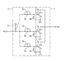
In the gate bias circuit 2, each resistor 4 a, 4 b or 4 c is connected between gate terminals of the FET cell 3 a, 3 b or 3 c and grounding terminals, respectively. The grounding terminals are terminals to ground the power amplifier according to the present first embodiment. One ends of resistors 5 a, 5 b and 5 c are connected to the gate terminals of the FET cells 3 a, 3 b and 3 c, respectively and other ends thereof are connected to each other. A connection point of the other ends of the resistors 5 a, 5 b and 5 c is connected to an input terminal IN to which an RF signal is inputted. Capacitors 6 a, 6 b and 6 c are connected in parallel to the resistors 5 a, 5 b and 5 c, respectively. The capacitors 6 a, 6 b and 6 c have capacitance values close to those of short circuit at their operating frequencies and bypass an RF signal.
A resistor 7 is connected between the connection point of the other ends of the resistors 5 a, 5 b and 5 c, and a power supply terminal 8. Here, the power supply terminal 8 is a terminal to connect the power amplifiers according to the present first embodiment to an external power supply, and when a negative voltage Vgg is applied to the power supply terminal 8, a gate voltage is supplied to the gate terminal of each FET cell 3 a, 3 b or 3 c. The resistors are made up of metal resistors, the capacitors are made up of MIMs, and these are integrated as an MMIC.
The resistors 4 a, 4 b and 4 c have temperature coefficients of resistance greater than those of the resistors 5 a, 5 b and 5 c and the resistor 7, and are arranged closer to the corresponding FET cells 3 a, 3 b and 3 c than the resistor 7.
Next, the effects of the present embodiment will be described in comparison with a comparative example. FIG. 2 is a circuit diagram illustrating a power amplifier according to a comparative example. In the comparative example, one resistor 4 is connected between a combination of gate terminals of a plurality of FET cells 3 a, 3 b and 3 c and a grounding terminal. The resistor 4 is disposed spaced apart from the FET cells 3 a, 3 b and 3 c as in the case of the resistor 7.
In the comparative example, the resistor 4 connected between the gate terminals and the grounding terminal compensates gate voltages with respect to temperatures, but the gate voltages with respect to the respective FET cells 3 a, 3 b and 3 c are the same. Therefore, setting a large amount of reduction of the gate voltage with respect to a temperature rise is set to suppress thermal runaway of the center FET cell 3 b results in excessive compensation for the FET cells 3 a and 3 c at both ends.
In contrast, in the present embodiment, since the resistors 4 a, 4 b and 4 c are arranged at points closest to the respective FET cells 3 a, 3 b and 3 c, the resistance values of the resistors 4 a, 4 b and 4 c change according to heat generation of the respective FET cells 3 a, 3 b and 3 c. Therefore, the resistor 4 b corresponding to the FET cell 3 b at the center that results in a high temperature exhibits a relatively large resistance value, whereas the resistors 4 a and 4 c corresponding to the FET cells 3 a and 3 c at both ends exhibit relatively small resistance values. On the other hand, since the resistor 7 is disposed spaced apart from the FET cells 3 a, 3 b and 3 c, it is hardly susceptible to heat generated at the FET cells 3 a, 3 b and 3 c. Furthermore, since the resistors 5 a, 5 b and 5 c are connected in series to the gate terminals of the respective FET cells 3 a, 3 b and 3 c, different gate voltages are applied to the respective FET cells 3 a, 3 b and 3 c. At this time, the gate voltages applied to the respective FET cells 3 a, 3 b and 3 c depend on the resistance values of the resistors 4 a, 4 b and 4 c. For this reason, the gate voltage of the FET cell 3 b at the center is set to be relatively low and the gate voltages of the FET cells 3 a and 3 c at both ends are set to be relatively high.
As described above, in the present embodiment, the resistors 4 a, 4 b and 4 c having greater temperature coefficients of resistance than the resistors 5 a, 5 b and 5 c, and the resistor 7 are connected between the gate terminals of the FET cells 3 a, 3 b, and 3 c, and their respective grounding terminals correspondingly, and arranged closer to the corresponding FET cells 3 a, 3 b and 3 c than the resistor 7. This makes it possible to appropriately set the gate voltages in accordance with the temperatures of the respective FET cells 3 a, 3 b and 3 c, and thereby suppress thermal runaway even when the plurality of FET cells 3 a, 3 b and 3 c are connected in parallel.
Note that the temperature coefficients of the resistors 4 a, 4 b and 4 c are preferably set in accordance with the temperature dependency of the gate leakage current of the FET 1. When the temperature dependency of the gate leakage current of the FET 1 is large, the gate voltage rise due to a temperature rise is also large, and therefore the temperature coefficient among the resistors 4 a, 4 b and 4 c needs also be set to a large value. Furthermore, when the temperature difference according to the positions of the FET cells 3 a, 3 b and 3 c is large, the gate voltage difference among the respective FET cells 3 a, 3 b and 3 c needs to be set to a large value. In this case, by setting the resistance values of the resistors 5 a, 5 b and 5 c to be greater than the resistance values of the resistors 4 a, 4 b and 4 c, it is possible to increase the potential difference among the gate terminals of the respective FET cells 3 a, 3 b and 3 c.
Second Embodiment
In the first embodiment, only the resistors 4 a, 4 b and 4 c are arranged at positions closest to the FET cells 3 a, 3 b and 3 c. In contrast, in the present embodiment, the resistors 5 a, 5 b and 5 c are epitaxial layer resistors that have negative temperature coefficients of resistance smaller than the temperature coefficient of the resistor 7 and are arranged closer to the corresponding FET cells 3 a, 3 b and 3 c than the resistor 7.
At a high temperature, the gate leakage current increases and flows into the resistors 5 a, 5 b and 5 c, causing the gate voltages of the FET cells 3 a, 3 b and 3 c to increase. However, in the present embodiment, since the resistance values of the resistors 5 a, 5 b and 5 c decrease at a high temperature, it is possible to suppress increases in the gate voltages. Furthermore, when there is a temperature difference among the FET cells 3 a, 3 b and 3 c, the resistor 5 b connected to the FET cell 3 b which has a higher temperature exhibits a smaller resistance value than those of the resistors 5 a and 5 c, and therefore the gate voltage of the FET cell 3 b is set to be lower than those of the FET cells 3 a and 3 c. As a result, it is possible to suppress thermal runaway more reliably than the first embodiment.
Furthermore, the resistors 5 a, 5 b and 5 c are epitaxial layer resistors. While a temperature coefficient of a metal resistor is determined substantially by its material, the temperature coefficient of resistance of the epitaxial layer resistor is changed according to an epitaxial layer concentration, and it is thereby possible to obtain a desired temperature coefficient. Therefore, it is possible to widen a range of adjustment of the gate voltages of the respective FET cells 3 a, 3 b and 3 c with respect to the temperature changes of the FET cells 3 a, 3 b and 3 c.
Note that the resistors 5 a, 5 b and 5 c may be configured to include metal resistors having positive temperature coefficients of resistance and epitaxial layer resistors connected in series to the metal resistors and having negative temperature coefficients of resistance. This makes it possible to obtain a desired temperature coefficient by changing the respective resistance ratios.
Third Embodiment
As the temperature of the FET 1 increases, the gate leakage current increases accordingly, but the resistance values of the resistors 5 a, 5 b and 5 c connected to the gate terminals decrease, causing the gate voltage to decrease. For this reason, it is possible to suppress thermal runaway at a high temperature. Furthermore, since the gate voltages can be set appropriately in accordance with the temperatures of the respective FET cells 3 a, 3 b and 3 c, it is possible to suppress thermal runaway even when a plurality of FET cells 3 a, 3 b and 3 c are connected in parallel. Furthermore, since the resistors 4 a, 4 b and 4 c become unnecessary, it is possible to downsize the apparatus more than in the first embodiment.
Obviously many modifications and variations of the present invention are possible in the light of the above teachings. It is therefore to be understood that within the scope of the appended claims the invention may be practiced otherwise than as specifically described.
The entire disclosure of Japanese Patent Application No. 2016-006192, filed on Jan. 15, 2016 including specification, claims, drawings and summary, on which the Convention priority of the present application is based, is incorporated herein by reference in its entirety.
Claims (4)
1. A power amplifier comprising:
a plurality of FET cells connected in parallel to each other;
a plurality of first resistors connected between gate terminals of the plurality of FET cells and grounding terminals respectively;
a plurality of second resistors having one ends connected to the gate terminals of the plurality of FET cells respectively and other ends connected to each other;
a plurality of capacitors connected in parallel to the plurality of second resistors respectively; and
a third resistor connected between a connection point of the other ends of the plurality of second resistors and a power supply terminal,
wherein the first resistors have temperature coefficients of resistance greater than those of the second and third resistors and are arranged closer to the corresponding FET cells than the third resistor.
2. The power amplifier of claim 1 , wherein the second resistors have negative temperature coefficients of resistance and are arranged closer to the corresponding FET cells than the third resistor.
3. The power amplifier of claim 2 , wherein the second resistors include metal resistors having positive temperature coefficients of resistance and epitaxial layer resistors connected in series to the metal resistors and having negative temperature coefficients of resistance.
4. A power amplifier comprising:
a plurality of FET cells connected in parallel to each other;
a plurality of first resistors having one ends connected to gate terminals of the plurality of FET cells respectively and other ends connected to each other;
a plurality of capacitors connected in parallel to the plurality of first resistors respectively; and
a second resistor connected between a connection point of the other ends of the plurality of first resistors and a power supply terminal,
wherein the first resistors have temperature coefficients of resistance greater than that of the second resistor and are arranged closer to the corresponding FET cells than the second resistor.
Applications Claiming Priority (2)
| Application Number | Priority Date | Filing Date | Title |
|---|---|---|---|
| JP2016006192A JP6547636B2 (en) | 2016-01-15 | 2016-01-15 | Power amplifier |
| JP2016-006192 | 2016-01-15 |
Publications (2)
| Publication Number | Publication Date |
|---|---|
| US20170207753A1 US20170207753A1 (en) | 2017-07-20 |
| US9800210B2 true US9800210B2 (en) | 2017-10-24 |
Family
ID=59256059
Family Applications (1)
| Application Number | Title | Priority Date | Filing Date |
|---|---|---|---|
| US15/249,680 Active US9800210B2 (en) | 2016-01-15 | 2016-08-29 | Power amplifier including a plurality of FET cells connected in parallel |
Country Status (4)
| Country | Link |
|---|---|
| US (1) | US9800210B2 (en) |
| JP (1) | JP6547636B2 (en) |
| CN (1) | CN107026623B (en) |
| DE (1) | DE102017200247B4 (en) |
Families Citing this family (2)
| Publication number | Priority date | Publication date | Assignee | Title |
|---|---|---|---|---|
| CN110553747A (en) * | 2019-08-30 | 2019-12-10 | 华为技术有限公司 | device, method and system for detecting thermal runaway of electrical equipment |
| JP7384318B1 (en) | 2022-11-10 | 2023-11-21 | 三菱電機株式会社 | power amplifier |
Citations (10)
| Publication number | Priority date | Publication date | Assignee | Title |
|---|---|---|---|---|
| JPH0832087A (en) | 1994-07-21 | 1996-02-02 | Toshiba Corp | Integrated circuit |
| JPH11297941A (en) | 1998-04-09 | 1999-10-29 | Nec Corp | Semiconductor device |
| US6018270A (en) * | 1993-07-12 | 2000-01-25 | Intersil Corporation | Low voltage RF amplifier and mixed with single bias block and method |
| JP2000209038A (en) | 1998-11-12 | 2000-07-28 | Hitachi Ltd | High frequency power amplifier and radio communication equipment |
| JP2000349563A (en) | 1999-06-02 | 2000-12-15 | Matsushita Electric Ind Co Ltd | Power amplifier |
| US6329879B1 (en) | 1998-11-12 | 2001-12-11 | Hitachi, Ltd. | High frequency power amplifier system and wireless communication system |
| WO2006057104A1 (en) | 2004-11-29 | 2006-06-01 | Murata Manufacturing Co., Ltd. | Semiconductor device and power amplifier |
| US20070222033A1 (en) | 2004-11-29 | 2007-09-27 | Murata Manufacturing Co., Ltd. | Semiconductor device and power amplifier |
| US20110018639A1 (en) | 2009-07-27 | 2011-01-27 | Mitsubishi Electric Corporation | Power amplifier bias circuit |
| JP2013207408A (en) | 2012-03-27 | 2013-10-07 | Panasonic Corp | Power amplifier |
Family Cites Families (4)
| Publication number | Priority date | Publication date | Assignee | Title |
|---|---|---|---|---|
| US6147481A (en) * | 1996-12-27 | 2000-11-14 | Emc Technology Llc | Termination for RF circuit which senses changes in power and which is not temperature sensitive |
| CN100488062C (en) * | 2000-10-18 | 2009-05-13 | 中兴通讯股份有限公司 | Gain temperature compensator for transceiver |
| JP2005216943A (en) * | 2004-01-27 | 2005-08-11 | Murata Mfg Co Ltd | Semiconductor device and power amplifier using it |
| JP6036937B2 (en) | 2015-08-03 | 2016-11-30 | セイコーエプソン株式会社 | Method for producing metal powder, method for producing ultraviolet curable ink jet composition, and method for producing recorded matter |
-
2016
- 2016-01-15 JP JP2016006192A patent/JP6547636B2/en active Active
- 2016-08-29 US US15/249,680 patent/US9800210B2/en active Active
-
2017
- 2017-01-10 DE DE102017200247.6A patent/DE102017200247B4/en active Active
- 2017-01-13 CN CN201710024873.XA patent/CN107026623B/en active Active
Patent Citations (12)
| Publication number | Priority date | Publication date | Assignee | Title |
|---|---|---|---|---|
| US6018270A (en) * | 1993-07-12 | 2000-01-25 | Intersil Corporation | Low voltage RF amplifier and mixed with single bias block and method |
| JPH0832087A (en) | 1994-07-21 | 1996-02-02 | Toshiba Corp | Integrated circuit |
| JPH11297941A (en) | 1998-04-09 | 1999-10-29 | Nec Corp | Semiconductor device |
| US6046481A (en) | 1998-04-09 | 2000-04-04 | Nec Corporation | Transistor for preventing a thermal runaway caused by temperature rise in a bias circuit of the transistor |
| JP2000209038A (en) | 1998-11-12 | 2000-07-28 | Hitachi Ltd | High frequency power amplifier and radio communication equipment |
| US6329879B1 (en) | 1998-11-12 | 2001-12-11 | Hitachi, Ltd. | High frequency power amplifier system and wireless communication system |
| JP2000349563A (en) | 1999-06-02 | 2000-12-15 | Matsushita Electric Ind Co Ltd | Power amplifier |
| WO2006057104A1 (en) | 2004-11-29 | 2006-06-01 | Murata Manufacturing Co., Ltd. | Semiconductor device and power amplifier |
| US20070222033A1 (en) | 2004-11-29 | 2007-09-27 | Murata Manufacturing Co., Ltd. | Semiconductor device and power amplifier |
| US20110018639A1 (en) | 2009-07-27 | 2011-01-27 | Mitsubishi Electric Corporation | Power amplifier bias circuit |
| JP2011030006A (en) | 2009-07-27 | 2011-02-10 | Mitsubishi Electric Corp | Bias circuit for power amplifier |
| JP2013207408A (en) | 2012-03-27 | 2013-10-07 | Panasonic Corp | Power amplifier |
Also Published As
| Publication number | Publication date |
|---|---|
| JP6547636B2 (en) | 2019-07-24 |
| CN107026623A (en) | 2017-08-08 |
| JP2017126950A (en) | 2017-07-20 |
| DE102017200247A1 (en) | 2017-07-20 |
| US20170207753A1 (en) | 2017-07-20 |
| CN107026623B (en) | 2020-08-07 |
| DE102017200247B4 (en) | 2022-05-05 |
Similar Documents
| Publication | Publication Date | Title |
|---|---|---|
| US20110127849A1 (en) | high-power tunable capacitor | |
| CN108933574B (en) | Power amplifying circuit | |
| US9344044B2 (en) | High-frequency power amplifier | |
| US8217722B2 (en) | Power amplifier | |
| US20220006427A1 (en) | Amplifier circuit and amplifier device | |
| US11038465B2 (en) | Amplifier linearity boost circuits and methods for post distortion feedback cancelation | |
| US11290060B2 (en) | Bias circuit | |
| US20200266763A1 (en) | Bias circuit | |
| US9800210B2 (en) | Power amplifier including a plurality of FET cells connected in parallel | |
| US11469718B2 (en) | Amplifier circuit | |
| US11489495B2 (en) | Cascode gain boosting and linear gain control using gate resistor | |
| US11652451B2 (en) | Power amplifier device | |
| US10033333B2 (en) | Universal RF amplifier controller | |
| CN110739917A (en) | Temperature compensation circuit based on radio frequency power amplifier | |
| US11614759B2 (en) | Leakage compensation circuit | |
| CN107070439B (en) | Semiconductor device with a plurality of semiconductor chips | |
| US10862435B2 (en) | Impedance circuit and bias circuit | |
| US20200050230A1 (en) | Circuit arrangement for compensating current variations in current mirror circuit | |
| US8044720B2 (en) | Amplification circuit | |
| CN113748598B (en) | Amplifying circuit and amplifying device | |
| US9297840B2 (en) | Power detection circuit | |
| US20240072731A1 (en) | Over temperature protection with soft shutdown for power amplifier | |
| KR20150058932A (en) | Bias circuit using negative voltage |
Legal Events
| Date | Code | Title | Description |
|---|---|---|---|
| AS | Assignment |
Owner name: MITSUBISHI ELECTRIC CORPORATION, JAPAN Free format text: ASSIGNMENT OF ASSIGNORS INTEREST;ASSIGNORS:KATO, KATSUYA;KOSAKA, NAOKI;FUKUDA, ERI;AND OTHERS;SIGNING DATES FROM 20160615 TO 20160617;REEL/FRAME:039610/0761 |
|
| STCF | Information on status: patent grant |
Free format text: PATENTED CASE |
|
| MAFP | Maintenance fee payment |
Free format text: PAYMENT OF MAINTENANCE FEE, 4TH YEAR, LARGE ENTITY (ORIGINAL EVENT CODE: M1551); ENTITY STATUS OF PATENT OWNER: LARGE ENTITY Year of fee payment: 4 |