US8212886B2 - Interface converting circuit - Google Patents
Interface converting circuit Download PDFInfo
- Publication number
- US8212886B2 US8212886B2 US12/045,918 US4591808A US8212886B2 US 8212886 B2 US8212886 B2 US 8212886B2 US 4591808 A US4591808 A US 4591808A US 8212886 B2 US8212886 B2 US 8212886B2
- Authority
- US
- United States
- Prior art keywords
- signal
- pixel clock
- data
- synchronization signal
- flop
- Prior art date
- Legal status (The legal status is an assumption and is not a legal conclusion. Google has not performed a legal analysis and makes no representation as to the accuracy of the status listed.)
- Active, expires
Links
- 230000006835 compression Effects 0.000 claims abstract description 22
- 238000007906 compression Methods 0.000 claims abstract description 22
- 230000000873 masking effect Effects 0.000 claims abstract description 4
- 239000000872 buffer Substances 0.000 claims description 3
- 230000003111 delayed effect Effects 0.000 claims description 3
- 238000010586 diagram Methods 0.000 description 16
- 230000000630 rising effect Effects 0.000 description 4
- 238000000034 method Methods 0.000 description 2
- 238000012986 modification Methods 0.000 description 2
- 230000004048 modification Effects 0.000 description 2
- 239000004973 liquid crystal related substance Substances 0.000 description 1
Images


Classifications
-
- H—ELECTRICITY
- H04—ELECTRIC COMMUNICATION TECHNIQUE
- H04N—PICTORIAL COMMUNICATION, e.g. TELEVISION
- H04N7/00—Television systems
- H04N7/01—Conversion of standards, e.g. involving analogue television standards or digital television standards processed at pixel level
- H04N7/0117—Conversion of standards, e.g. involving analogue television standards or digital television standards processed at pixel level involving conversion of the spatial resolution of the incoming video signal
- H04N7/012—Conversion between an interlaced and a progressive signal
-
- H—ELECTRICITY
- H04—ELECTRIC COMMUNICATION TECHNIQUE
- H04N—PICTORIAL COMMUNICATION, e.g. TELEVISION
- H04N25/00—Circuitry of solid-state image sensors [SSIS]; Control thereof
-
- H—ELECTRICITY
- H04—ELECTRIC COMMUNICATION TECHNIQUE
- H04N—PICTORIAL COMMUNICATION, e.g. TELEVISION
- H04N23/00—Cameras or camera modules comprising electronic image sensors; Control thereof
- H04N23/80—Camera processing pipelines; Components thereof
- H04N23/81—Camera processing pipelines; Components thereof for suppressing or minimising disturbance in the image signal generation
Definitions
- the present invention relates to an interface converting circuit, and more particularly to an interface converting circuit applied between a 3D de-interlace chip and a rear-end image compression chip.
- FIG. 1 is a block diagram showing a conventional image processing system of an IP CAM.
- the IP CAM image processing system comprises: an image-capturing module 10 and a rear-end image compression chip 14 .
- the image-capturing module 10 further comprises a charge coupled device (CCD) and a digital signal processor (not shown).
- CCD charge coupled device
- the capturing signals When the CCD of the image-capturing module 10 is capturing an object, the capturing signals, generated by the CCD, is transmitted to the digital signal processor.
- the capturing signals are then transferred to pixel-format signals (i.e., resolution 720 ⁇ 480) by the digital signal processor.
- the digital signal processor then sequentially outputs an odd-field signal (resolution 720 ⁇ 240) and an even-field signal (resolution 720 ⁇ 240) according to the transferred pixel-format signals, wherein the odd-field signal is defined as the odd scanning lines of the CCD transmitted to the digital signal processor, and the even-field signal is defined as the even scanning lines of the CCD transmitted to the digital signal processor.
- the odd-field signal and the even-field signal derived from the image-capturing module 10 are then received and mixed to a complete frame (resolution 720 ⁇ 480) by the rear-end image compression chip 14 (i.e., MPEG-4/H.264 encoder).
- the generated frame is then further encoded and compressed by the rear-end image compression chip 14 .
- FIG. 3A shows an odd-field signal (resolution 10 ⁇ 4), which is constituted by odd scanning lines (scanning lines 1 , 3 , 5 , 7 ).
- FIG. 3B shows an even-field signal (resolution 10 ⁇ 4), which is constituted by even scanning lines (scanning lines 2 , 4 , 6 , 8 ).
- the odd-field signal and the even-field signal are sequentially received by the rear-end image compression chip 14 at time point t 1 and t 2 , respectively.
- the odd-field signal and the even-field signal are then mixed to a complete frame (resolution 10 ⁇ 8, depicted in FIG. 3C ), and the rear-end image compression chip 14 further encodes and compresses the complete frame.
- the image-capturing module 10 outputs the odd-field signal and the even-field signal with the same frame rate of 30 frames per second (30 FPS).
- a saw tooth type edge distortion may be resulted in due to each complete frame is mixed by two field signals.
- an odd-field signal (resolution 10 ⁇ 4, depicted in FIG. 4A ) is derived from the image-capturing module 10 at time point t 1 ; and an even-field signal (resolution 10 ⁇ 4, depicted in FIG. 4B ) is derived from the image-capturing module 10 at time point t 2 .
- the saw tooth type edge distortion is occurred in the complete frame (resolution 10 ⁇ 8, depicted in FIG. 4C ) if the odd-filed signal (depicted in FIG. 4A ) and the even-field signal (depicted in FIG. 4B ) are mixed (or interlaced) to a complete frame.
- the saw tooth type edge distortion resulted from an interlace CCD scanning a fast-moving object, can be avoided by introducing a 3D de-interlace chip in the image processing system. Instead of mixing the odd-filed signal and the even-field signal, the image processing system with the 3D de-interlace chip generates a complete frame through executing dynamic prediction compensation to each odd-filed signal and each even-field signal. In another word, when the odd-field signal (resolution 720 ⁇ 240) is generated at time point t 1 , the 3D de-interlace chip generates a complete frame (resolution 720 ⁇ 480) through executing the dynamic prediction compensation to the odd-field signal.
- the 3D de-interlace chip when the even-field signal (resolution 720 ⁇ 240) is generated at time point t 2 , the 3D de-interlace chip generates another complete frame (resolution 720 ⁇ 480) through executing the dynamic prediction compensation to the even-field signal.
- the image processing system with the 3D de-interlace chip not only the saw tooth type edge distortion resulted from the mixing procedure is avoided, but also the number of the generated frames is doubled.
- the output specification of the 3D de-interlace chip must be compatible of the input specification of the LCDTV.
- the 3D de-interlace chip is designed to output data with 16 bits data width and output data with a frame rate of 60 frames per second (60 FPS).
- the input specification of the rear-end image compression chip i.e., MPEG-4/H.264 encoder
- MPEG-4/H.264 encoder is designed to receive 8 bits data width and receives data with a frame rate of 30 frames per second (30 FPS). Therefore, designing an interface converting circuit for the compatibility between the 3D de-interlace chip and the rear-end image compression chip is the main purpose of the present invention.
- the object of the present invention is to provide an interface converting circuit for the compatibility between the 3D de-interlace chip and the rear-end image compression chip
- the present invention provides an interface converting circuit, applied between a 3D de-interlace chip and a rear-end image compression chip, comprising: a reducing FPS circuit, for dividing a first vertical synchronization signal to generate a second vertical synchronization signal, and converting a first horizontal synchronization signal to a second horizontal synchronization signal by masking the first horizontal synchronization signal according to the second vertical synchronization signal; a pixel clock multiplier, for multiplying a first pixel clock signal to generate a second pixel clock signal; and, a data-width converter, for converting an input signal with M bits data width, which is transmitted at a frequency of the first pixel clock signal by the 3D de-interlace chip, to an output signal with M/2 bits data width, which is transmitted at a frequency of the second pixel clock signal.
- a reducing FPS circuit for dividing a first vertical synchronization signal to generate a second vertical synchronization signal, and converting a first horizontal synchronization signal to a second horizontal synchronization
- FIG. 1 is a block diagram showing a conventional image processing system of an IP CAM.
- FIG. 2 illustrates a still object captured by CCD.
- FIG. 3A shows an odd-field signal of FIG. 2 .
- FIG. 3B shows an even-field signal of FIG. 2 .
- FIG. 3C shows a complete frame
- FIG. 4A shows an odd-field signal of a moving object.
- FIG. 4B shows an even-field signal of the moving object.
- FIG. 4C shows a combination frame of the odd-field signal and the even field signal.
- FIG. 5 is a block diagram showing an image processing system.
- FIG. 6 is a schematic diagram showing a circuit configuration of the reducing FPS circuit.
- FIG. 7A is a timing diagram showing the relationship of Vsync_in and Vsync_out.
- FIG. 7B is a timing diagram showing the relationships of the Vsync_in, Hsync_in, and Hsync_out.
- FIG. 8 is a schematic diagram showing the circuit configuration of the pixel clock multiplier.
- FIG. 9 is a timing diagram showing the relationships of the PixelClock_in, the delayed pixel clock signal, and the outputted pixel clock signal an inputted pixel clock signal (PixelClock_out)
- FIG. 10 is a schematic diagram showing the circuit configuration of the data-width converter.
- FIG. 5 is a block diagram showing an image processing system.
- the image processing system comprises: a 3D de-interlace chip 16 (CCIR601 specification), a rear-end image compression chip 14 (i.e., MPEG-4/H.264 encoder), and an interface converting circuit 18 of the present invention.
- the interface converting circuit 18 further comprises: a reducing FPS circuit 182 , a pixel clock multiplier 184 , and a data-width converter 186 .
- the CbCr signal is transmitted from the lower eight bits [D 0 :D 7 ], and the Y signal is transmitted from the higher eight bits [D 8 :D 15 ].
- an inputted vertical synchronization signal (Vsync_in), an inputted horizontal synchronization signal (Hsync_in), and an inputted pixel clock signal (PixelClock_in) are also derived from the 3D de-interlace chip 16 .
- the frequency of the inputted vertical synchronization signal (Vsync_in) is 60 Hz standing for the 3D de-interlace chip 16 to transmit 60 frames per second (60 FPS).
- the inputted horizontal synchronization signal (Hsync_in) stands for the number of the horizontal-scanning lines contained in each image.
- the frequency of the horizontal synchronization signal (Hsync_in) is 28800(60 ⁇ 480) Hz if an image is with a resolution 720 ⁇ 480.
- the inputted pixel clock signal (PixelClock_in) stands for the sample numbers in each scanning line. In the embodiment, the frequency of the inputted pixel clock signal (PixelClock_in) is 27 MHz.
- the main function of the reducing FPS circuit 182 in the interface converting circuit 18 of the present invention is to reduce the frame rate of the 3D de-interlace chip 16 (CCIR601 specification) from 60 FPS to 30 FPS.
- FIG. 6 is a schematic diagram showing a circuit configuration of the reducing FPS circuit 182 in the interface converting circuit 18 of the present invention.
- the reducing FPS circuit 182 comprises: a T-type Flip-Flop (FTC) and an AND gate (AND_G).
- a data-input terminal (T) of the T-type Flip-Flop (FTC) is connected to a voltage source (Vcc); a clock terminal (C) of the T-type Flip-Flop (FTC) serves to receive the inputted vertical synchronization signal (Vsync_in) which is derived from the 3D de-interlace chip 16 ; a clear terminal (CLR) of the T-type Flip-Flop (FTC) is connected to ground (GND); a first input terminal of the AND gate (AND_G) is connected to a data output terminal (Q) of the T-type Flip-Flop (FTC), a second input terminal of the AND gate (AND_G) serves to receive the inputted horizontal synchronization signal (Hsync_in) which is derived from the 3D de-interlace chip 16 .
- the output terminal (Q) of the T-type Flip-Flop (FTC) can change its level at the rising edges of the inputted vertical synchronization signal (Vsync_in). That means the inputted vertical synchronization signal (Vsync_in) is divided by two to generate the outputted vertical synchronization signal (Vsync_out).
- FIG. 7A is a timing diagram showing the relationship of inputted vertical synchronization signal (Vsync_in) and the outputted vertical synchronization signal (Vsync_out).
- the frequency of the inputted vertical synchronization signal (Vsync_in) is 60 Hz and the outputted vertical synchronization signal (Vsync_out) is 30 Hz.
- FIG. 7B is a timing diagram showing the relationships of the outputted vertical synchronization signal Vsync_out, the inputted horizontal synchronization signal (Hsync_in), and the outputted horizontal synchronization signal (Hsync_out). Because the outputted vertical synchronization signal (Vsync_out) and the inputted horizontal synchronization signal (Hsync_in) are received by the AND gate (AND_G), the outputted horizontal synchronization signal (Hsync_out) is generated by masking half pulses of the inputted horizontal synchronization signal (Hsync_in) and derived from the output terminal of the AND gate (AND_G).
- the pixel clock is 27 MHz and the output data width is 16 bits.
- the rear-end image compression chip 14 i.e., MPEG-4/H.264 encoder
- the pixel clock multiplier 184 has to increase the pixel clock (54 MHz) and the data-width converter 186 has to decrease the 16 bits data width to the 8 bits data width, so as the data derived from the 3D de-interlace chip 16 (CCIR601 specification) can be completely processed by the rear-end image compression chip 14 (i.e., MPEG-4/H.264 encoder) in time.
- FIG. 8 is a schematic diagram showing the circuit configuration of the pixel clock multiplier 184 in the interface converting circuit 18 of the present invention.
- the pixel clock multiplier 184 comprises: a XOR gate (XOR_G) and a delay component 188 .
- the inputted pixel clock signal (PixelClock_in) with 27 MHz derived from the 3D de-interlace chip 16 is derived to a first input terminal of the XOR gate (XOR_G) and an input terminal of the delay component 188 ; an output terminal of the delay component 188 is connected to a second input terminal of the XOR gate (XOR_G);
- the delay component 188 constituted by a plurality of buffers (BUF) coupled in series, serves to delay the inputted pixel clock signal (PixelClock_in) 1 ⁇ 4 clock cycle.
- FIG. 9 is a timing diagram showing the relationships of the inputted pixel clock signal (PixelClock_in), the delayed pixel clock signal, and the outputted pixel clock signal (PixelClock_out) derived from the XOR gate (XOR_G).
- the frequency of the pixel clock signal (27 MHz) derived to the pixel clock multiplier 184 is doubled to 54 MHz and derived from the output terminal of the XOR gate (XOR_G).
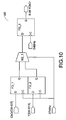
- FIG. 10 is a schematic diagram showing the circuit configuration of the data-width converter 186 .
- the data-width converter 186 comprises: a first D-type Flip-Flop (FD_ 1 ), a second D-type Flip-Flop (FD_ 2 ), a third D-type Flip-Flop (FD_ 3 ), and a multiplexer (M 2 _ 1 ).
- a data input terminal (D) of the first D-type Flip-Flop (FD_ 1 ) serves to receive lower eight bits data (8-bit CbCr signal [D 0 :D 7 ]); a clock terminal (C) of the first D-type Flip-Flop (FD_ 1 ) serves to receive the inputted pixel clock signal (PixelClock_in, 27 MHz); a data input terminal (D) of the second D-type Flip-Flop (FD_ 2 ) serves to receive higher eight bits data (8-bit Y signal [D 8 :D 15 ]); a clock terminal (C) of the second D-type Flip-Flop (FD_ 2 ) serves to receive the inputted pixel clock signal (PixelClock_in, 27 MHz); a first input terminal of the multiplexer (M 2 _ 1 ) is connected to an output terminal (Q) of the first D-type Flip-Flop (FD_ 1 ); a second input terminal of the multiplexer
- the lower eight bits data (8-bit CbCr signal [D 0 :D 7 ]) is further transmitted to the output terminal of the multiplexer (M 2 _ 1 ) and received by the third D-type Flip-Flop (FD_ 3 ) when the inputted pixel clock signal (PixelClock_in, 27 MHz) is at the high-level.
- the higher eight bits data (8-bit Y signal [D 8 :D 15 ]) is further transmitted to the output terminal of the multiplexer (M 2 _ 1 ) and received by the third D-type Flip-Flop (FD_ 3 ) when the inputted pixel clock signal (PixelClock_in, 27 MHz) is at the low-level.
- the lower eight bits data (8-bit CbCr signal [D 0 :D 7 ]) and the higher eight bits data (8-bit Y signal [D 0 :D 7 ]) are sequentially derived to the data input terminal (D) of the third Flip-Flop (FD_ 3 ) in one cycle of the inputted pixel clock signal (PixelClock_in).
- the lower eight bits data (8-bit CbCr signal [D 0 :D 7 ]) is further derived from the output terminal (Q) of the third Flip-Flop (FD_ 3 ) at the first rising edge of the outputted pixel clock signal (PixelClock_out, 54 MHz).
- the higher eight bits data (8-bit Y signal [D 8 :D 15 ]) is further derived from the output terminal (Q) of the third Flip-Flop (FD_ 3 ) at the second rising edge of the outputted pixel clock signal (PixelClock_out, 54 MHz).
- the lower eight bits data (8-bit CbCr signal [D 0 :D 7 ]) and the higher eight bits data (8-bit Y signal [D 0 :D 7 ]) are sequentially derived from the output terminal (Q) of the third Flip-Flop (FD_ 3 ) in two cycles of the outputted pixel clock signal (PixelClock_out).
- all the data derived from the 3D de-interlace chip 16 can be guaranteed to be delivered to the rear-end image compression chip 14 (i.e., MPEG-4/H.264 encoder) in time, so as the real-time performance can be achieved.
- the incompatible problem between the signals derived from the 3D de-interlace chip 16 (16 bits data width, 60 FPS) and the signals derived in the rear-end image compression chip 14 (8 bits data width, 30 FPS) can be solved by the interface converting circuit 18 of the present invention.
Abstract
Description
Claims (19)
Applications Claiming Priority (3)
| Application Number | Priority Date | Filing Date | Title |
|---|---|---|---|
| TW096129271 | 2007-08-08 | ||
| TW096129271A TWI348821B (en) | 2007-08-08 | 2007-08-08 | Interface converting circuit |
| TW96129271A | 2007-08-08 |
Publications (2)
| Publication Number | Publication Date |
|---|---|
| US20090040373A1 US20090040373A1 (en) | 2009-02-12 |
| US8212886B2 true US8212886B2 (en) | 2012-07-03 |
Family
ID=40346119
Family Applications (1)
| Application Number | Title | Priority Date | Filing Date |
|---|---|---|---|
| US12/045,918 Active 2031-05-04 US8212886B2 (en) | 2007-08-08 | 2008-03-11 | Interface converting circuit |
Country Status (3)
| Country | Link |
|---|---|
| US (1) | US8212886B2 (en) |
| JP (1) | JP4756060B2 (en) |
| TW (1) | TWI348821B (en) |
Families Citing this family (7)
| Publication number | Priority date | Publication date | Assignee | Title |
|---|---|---|---|---|
| JP2018028559A (en) * | 2015-01-07 | 2018-02-22 | シャープ株式会社 | Image data output device, image data output method, image display device, and integrated circuit |
| CN107526024B (en) * | 2017-08-17 | 2020-07-31 | 上海华岭集成电路技术股份有限公司 | Detection interface simplification conversion device |
| CN107888863B (en) * | 2017-11-29 | 2020-02-14 | 中国航空工业集团公司洛阳电光设备研究所 | Frame extraction method for converting ultrahigh frame frequency image stream into standard analog video stream |
| US10601425B2 (en) | 2018-05-30 | 2020-03-24 | Intel Corporation | Width and frequency conversion with PHY layer devices in PCI-express |
| US11467999B2 (en) | 2018-06-29 | 2022-10-11 | Intel Corporation | Negotiating asymmetric link widths dynamically in a multi-lane link |
| US10846247B2 (en) | 2019-03-05 | 2020-11-24 | Intel Corporation | Controlling partial link width states for multilane links |
| US11836101B2 (en) | 2019-11-27 | 2023-12-05 | Intel Corporation | Partial link width states for bidirectional multilane links |
Citations (8)
| Publication number | Priority date | Publication date | Assignee | Title |
|---|---|---|---|---|
| US6580461B2 (en) * | 1997-09-30 | 2003-06-17 | Koninklijke Philips Electronics N.V. | Line-quadrupler in home theater uses line-doubler of AV-part and scaler in graphics controller of PC-part |
| JP2003189262A (en) | 2001-10-20 | 2003-07-04 | Trident Microsystems Inc | Method for integrating three-dimensional y/c comb line filter and interlace/progressive converter into single chip and system thereof |
| CN2819683Y (en) | 2005-09-01 | 2006-09-20 | 上海欣泰通信技术有限公司 | Digital video conversion interface module |
| US20060285010A1 (en) * | 2005-06-17 | 2006-12-21 | Lsi Logic Corporation | Systems and methods for deinterlacing video signals |
| US20080211959A1 (en) * | 2007-01-05 | 2008-09-04 | Nikhil Balram | Methods and systems for improving low-resolution video |
| US7468754B2 (en) * | 2002-07-05 | 2008-12-23 | Thomson Licensing | High-definition de-interlacing and frame doubling circuit and method |
| US20110032331A1 (en) * | 2009-08-07 | 2011-02-10 | Xuemin Chen | Method and system for 3d video format conversion |
| US20110181691A1 (en) * | 2010-01-27 | 2011-07-28 | Sunplus Technology Co., Ltd. | System and method for decoding and de-interlacing CVBS signal |
Family Cites Families (2)
| Publication number | Priority date | Publication date | Assignee | Title |
|---|---|---|---|---|
| TWI223960B (en) * | 2003-05-02 | 2004-11-11 | Avermedia Tech Inc | Method and apparatus for equipping personal digital product with functions of recording and displaying of the digital video/audio multi-media |
| JP2006157720A (en) * | 2004-11-30 | 2006-06-15 | Toshiba Corp | Digital camera apparatus |
-
2007
- 2007-08-08 TW TW096129271A patent/TWI348821B/en active
-
2008
- 2008-03-11 US US12/045,918 patent/US8212886B2/en active Active
- 2008-07-08 JP JP2008178393A patent/JP4756060B2/en active Active
Patent Citations (8)
| Publication number | Priority date | Publication date | Assignee | Title |
|---|---|---|---|---|
| US6580461B2 (en) * | 1997-09-30 | 2003-06-17 | Koninklijke Philips Electronics N.V. | Line-quadrupler in home theater uses line-doubler of AV-part and scaler in graphics controller of PC-part |
| JP2003189262A (en) | 2001-10-20 | 2003-07-04 | Trident Microsystems Inc | Method for integrating three-dimensional y/c comb line filter and interlace/progressive converter into single chip and system thereof |
| US7468754B2 (en) * | 2002-07-05 | 2008-12-23 | Thomson Licensing | High-definition de-interlacing and frame doubling circuit and method |
| US20060285010A1 (en) * | 2005-06-17 | 2006-12-21 | Lsi Logic Corporation | Systems and methods for deinterlacing video signals |
| CN2819683Y (en) | 2005-09-01 | 2006-09-20 | 上海欣泰通信技术有限公司 | Digital video conversion interface module |
| US20080211959A1 (en) * | 2007-01-05 | 2008-09-04 | Nikhil Balram | Methods and systems for improving low-resolution video |
| US20110032331A1 (en) * | 2009-08-07 | 2011-02-10 | Xuemin Chen | Method and system for 3d video format conversion |
| US20110181691A1 (en) * | 2010-01-27 | 2011-07-28 | Sunplus Technology Co., Ltd. | System and method for decoding and de-interlacing CVBS signal |
Also Published As
| Publication number | Publication date |
|---|---|
| JP4756060B2 (en) | 2011-08-24 |
| TWI348821B (en) | 2011-09-11 |
| TW200908555A (en) | 2009-02-16 |
| US20090040373A1 (en) | 2009-02-12 |
| JP2009044729A (en) | 2009-02-26 |
Similar Documents
| Publication | Publication Date | Title |
|---|---|---|
| US8212886B2 (en) | Interface converting circuit | |
| KR100765880B1 (en) | High frame rate high definition imaging system and method | |
| JP5008826B2 (en) | High-definition deinterlacing / frame doubling circuit and method thereof | |
| TW201501074A (en) | Image display system and image processing method | |
| CN1225120C (en) | Image processing device, image processing method, recording medium and program | |
| US6919929B1 (en) | Method and system for implementing a video and graphics interface signaling protocol | |
| CN1210947C (en) | Cemera device and electronic device having the cemera device | |
| US5850257A (en) | Noise reduction device employing a sample and hold circuit, and an image pickup device using the noise reduction device | |
| CN1698372A (en) | Image data conversion method, conversion circuit, and digital camera | |
| EP2131584A1 (en) | Interface converting circuit | |
| CN1332574A (en) | Signal processing apparatus and method | |
| US5047849A (en) | Image display apparatus with image turbulence suppression | |
| EP2495963A2 (en) | Video display apparatus and video processing method | |
| EP1401203B1 (en) | Method of realizing combination of multi-sets of multiple digital images and bus interface technique | |
| CN113612938A (en) | Multi-type adaptive resolution image conversion method and device | |
| CN101102490A (en) | Interface conversion circuit | |
| CN100484194C (en) | Interlaced image signal frequency multiplication method and device | |
| TW200839693A (en) | Video circuit and head-mounted lcos display device | |
| US9077841B2 (en) | Video processing apparatus and video processing method | |
| KR20050094445A (en) | Frame conversion method, frame conversion circuit, and electronic camera | |
| KR100933171B1 (en) | Non-memory semiconductor embodied graphic display function | |
| US5117286A (en) | Video signal and output device for freeze-frame video telephone | |
| WO2000065565A1 (en) | High resolution display controller with reduced working frequency requirement for the display data handling circuitry | |
| He et al. | De-interlacing and YUV 4: 2: 2 to 4: 2: 0 conversion on TMS320DM6446 using the resizer | |
| CN102118598B (en) | Device and method for processing videos |
Legal Events
| Date | Code | Title | Description |
|---|---|---|---|
| AS | Assignment |
Owner name: WPAT.,P.C., VIRGINIA Free format text: ASSIGNMENT OF ASSIGNORS INTEREST;ASSIGNOR:LO, CHUNG-MING;REEL/FRAME:020631/0188 Effective date: 20080218 |
|
| AS | Assignment |
Owner name: ALPHA NETWORKS INC., TAIWAN Free format text: CORRECTIVE ASSIGNMENT TO CORRECT THE CORRECT RECEIVING PARTY PREVIOUSLY RECORDED ON REEL 020631 FRAME 0188;ASSIGNOR:LO, CHUNG-MING;REEL/FRAME:020893/0345 Effective date: 20080218 Owner name: ALPHA NETWORKS INC., TAIWAN Free format text: CORRECTIVE ASSIGNMENT TO CORRECT THE CORRECT RECEIVING PARTY PREVIOUSLY RECORDED ON REEL 020631 FRAME 0188. ASSIGNOR(S) HEREBY CONFIRMS THE ASSIGNMENT;ASSIGNOR:LO, CHUNG-MING;REEL/FRAME:020893/0345 Effective date: 20080218 |
|
| FEPP | Fee payment procedure |
Free format text: PAYOR NUMBER ASSIGNED (ORIGINAL EVENT CODE: ASPN); ENTITY STATUS OF PATENT OWNER: LARGE ENTITY |
|
| STCF | Information on status: patent grant |
Free format text: PATENTED CASE |
|
| FPAY | Fee payment |
Year of fee payment: 4 |
|
| MAFP | Maintenance fee payment |
Free format text: PAYMENT OF MAINTENANCE FEE, 8TH YEAR, LARGE ENTITY (ORIGINAL EVENT CODE: M1552); ENTITY STATUS OF PATENT OWNER: LARGE ENTITY Year of fee payment: 8 |
|
| MAFP | Maintenance fee payment |
Free format text: PAYMENT OF MAINTENANCE FEE, 12TH YEAR, LARGE ENTITY (ORIGINAL EVENT CODE: M1553); ENTITY STATUS OF PATENT OWNER: LARGE ENTITY Year of fee payment: 12 |