US8206839B2 - Organic electroluminescent element - Google Patents
Organic electroluminescent element Download PDFInfo
- Publication number
- US8206839B2 US8206839B2 US11/542,550 US54255006A US8206839B2 US 8206839 B2 US8206839 B2 US 8206839B2 US 54255006 A US54255006 A US 54255006A US 8206839 B2 US8206839 B2 US 8206839B2
- Authority
- US
- United States
- Prior art keywords
- group
- light
- formula
- compound
- electroluminescent element
- Prior art date
- Legal status (The legal status is an assumption and is not a legal conclusion. Google has not performed a legal analysis and makes no representation as to the accuracy of the status listed.)
- Active, expires
Links
- 0 c1ccc(C(c2cccc2)c2cccc2)c1 Chemical compound c1ccc(C(c2cccc2)c2cccc2)c1 0.000 description 8
- ACRHROGYQQHDLK-UHFFFAOYSA-N CC(C)=O.CC(C)=S.CP(C)(C)=O.CS(C)(=O)=O.CS(C)=O.C[Ge](C)=O Chemical compound CC(C)=O.CC(C)=S.CP(C)(C)=O.CS(C)(=O)=O.CS(C)=O.C[Ge](C)=O ACRHROGYQQHDLK-UHFFFAOYSA-N 0.000 description 4
- AAAQKTZKLRYKHR-UHFFFAOYSA-N c1ccc(C(c2ccccc2)c2ccccc2)cc1 Chemical compound c1ccc(C(c2ccccc2)c2ccccc2)cc1 AAAQKTZKLRYKHR-UHFFFAOYSA-N 0.000 description 2
- YWJKRZQEGFEJDF-YWQSAXMBSA-N B.C.C.C.C1=CC=C([Si](C2=CC=CC=C2)(C2=CC=CC=C2)C2=CC=CC(C(OC3CCCCO3)C3=CC=CC([Si](C4=CC=CC=C4)(C4=CC=CC=C4)C4=CC=CC=C4)=C3)=C2)C=C1.C1=COCCC1.CO.ClCCl.Cl[Si](C1=CC=CC=C1)(C1=CC=CC=C1)C1=CC=CC=C1.IC1=CC=CC(C(OC2CCCCO2)C2=CC=CC(I)=C2)=C1.O=C(C1=CC=CC(I)=C1)C1=CC(I)=CC=C1.O=C(C1=CC=CC(I)=C1)C1=CC(I)=CC=C1.O=C(C1=CC=CC([Si](C2=CC=CC=C2)(C2=CC=CC=C2)C2=CC=CC=C2)=C1)C1=CC([Si](C2=CC=CC=C2)(C2=CC=CC=C2)C2=CC=CC=C2)=CC=C1.O=C(O)C(F)(F)F.OB(O)C1=C(C2=CC=CC=C2)C=CC=C1.OC(C1=CC=CC(I)=C1)C1=CC(I)=CC=C1.OC(C1=CC=CC([Si](C2=CC=CC=C2)(C2=CC=CC=C2)C2=CC=CC=C2)=C1)C1=CC([Si](C2=CC=CC=C2)(C2=CC=CC=C2)C2=CC=CC=C2)=CC=C1.[2HH] Chemical compound B.C.C.C.C1=CC=C([Si](C2=CC=CC=C2)(C2=CC=CC=C2)C2=CC=CC(C(OC3CCCCO3)C3=CC=CC([Si](C4=CC=CC=C4)(C4=CC=CC=C4)C4=CC=CC=C4)=C3)=C2)C=C1.C1=COCCC1.CO.ClCCl.Cl[Si](C1=CC=CC=C1)(C1=CC=CC=C1)C1=CC=CC=C1.IC1=CC=CC(C(OC2CCCCO2)C2=CC=CC(I)=C2)=C1.O=C(C1=CC=CC(I)=C1)C1=CC(I)=CC=C1.O=C(C1=CC=CC(I)=C1)C1=CC(I)=CC=C1.O=C(C1=CC=CC([Si](C2=CC=CC=C2)(C2=CC=CC=C2)C2=CC=CC=C2)=C1)C1=CC([Si](C2=CC=CC=C2)(C2=CC=CC=C2)C2=CC=CC=C2)=CC=C1.O=C(O)C(F)(F)F.OB(O)C1=C(C2=CC=CC=C2)C=CC=C1.OC(C1=CC=CC(I)=C1)C1=CC(I)=CC=C1.OC(C1=CC=CC([Si](C2=CC=CC=C2)(C2=CC=CC=C2)C2=CC=CC=C2)=C1)C1=CC([Si](C2=CC=CC=C2)(C2=CC=CC=C2)C2=CC=CC=C2)=CC=C1.[2HH] YWJKRZQEGFEJDF-YWQSAXMBSA-N 0.000 description 1
- KDYOULWFRSAOLF-DYCDLGHISA-K BCP.C1=CC2=C(C=C1)N(C1=CC=C(C3=CC=C(N4C5=C(C=CC=C5)C5=C4/C=C\C=C/5)C=C3)C=C1)C1=C2C=CC=C1.C1=CC2=CC=CN3=C2C(=C1)O[AlH]3.C1=CC=C(N(C2=CC=C(C3=CC=C(N(C4=CC=CC=C4)C4=CC=CC5=C4C=CC=C5)C=C3)C=C2)C2=CC=CC3=C2C=CC=C3)C=C1.CC1(C)C2=CC=CC3=N2[Pt@]2(C4=CC=CC=C43)C3=C(C=CC=C3)C3=CC=CC1=N32.CC1=CC=C2C=CC=C3O[Al](OC4=CC=C(C5=CC=CC=C5)C=C4)N1=C23.[2H]N=P Chemical compound BCP.C1=CC2=C(C=C1)N(C1=CC=C(C3=CC=C(N4C5=C(C=CC=C5)C5=C4/C=C\C=C/5)C=C3)C=C1)C1=C2C=CC=C1.C1=CC2=CC=CN3=C2C(=C1)O[AlH]3.C1=CC=C(N(C2=CC=C(C3=CC=C(N(C4=CC=CC=C4)C4=CC=CC5=C4C=CC=C5)C=C3)C=C2)C2=CC=CC3=C2C=CC=C3)C=C1.CC1(C)C2=CC=CC3=N2[Pt@]2(C4=CC=CC=C43)C3=C(C=CC=C3)C3=CC=CC1=N32.CC1=CC=C2C=CC=C3O[Al](OC4=CC=C(C5=CC=CC=C5)C=C4)N1=C23.[2H]N=P KDYOULWFRSAOLF-DYCDLGHISA-K 0.000 description 1
- ZMKNNCINXCXRIC-UHFFFAOYSA-N C1=CC=C(C2=CC(C3=CC=CC=C3)=C([Bi](C3=C(C4=CC=CC=C4)C=C(C4=CC=CC=C4)C=C3C3=CC=CC=C3)C3=C(C4=CC=CC=C4)C=C(C4=CC=CC=C4)C=C3C3=CC=CC=C3)C(C3=CC=CC=C3)=C2)C=C1.FC(F)(F)C1=CC(C(F)(F)F)=C(C(=S)C2=C(C(F)(F)F)C=C(C(F)(F)F)C=C2C(F)(F)F)C(C(F)(F)F)=C1.O=C(C1=C(C2=CC=CC=C2)C=CC=C1C1=CC=CC=C1)S(=O)C1=C(C2=CC=CC=C2)C=CC=C1C1=CC=CC=C1.O=[Se](C1=C(C2=CC=CC=C2)C=C(C2=CC=CC=C2)C=C1C1=CC=CC=C1)C1=C(C2=CC=CC=C2)C=C(C2=CC=CC=C2)C=C1C1=CC=CC=C1.S=C(C1=C(C2=CC=CC=C2)C=C(C2=CC=CC=C2)C=C1C1=CC=CC=C1)C1=C(C2=CC=CC=C2)C=C(C2=CC=CC=C2)C=C1C1=CC=CC=C1 Chemical compound C1=CC=C(C2=CC(C3=CC=CC=C3)=C([Bi](C3=C(C4=CC=CC=C4)C=C(C4=CC=CC=C4)C=C3C3=CC=CC=C3)C3=C(C4=CC=CC=C4)C=C(C4=CC=CC=C4)C=C3C3=CC=CC=C3)C(C3=CC=CC=C3)=C2)C=C1.FC(F)(F)C1=CC(C(F)(F)F)=C(C(=S)C2=C(C(F)(F)F)C=C(C(F)(F)F)C=C2C(F)(F)F)C(C(F)(F)F)=C1.O=C(C1=C(C2=CC=CC=C2)C=CC=C1C1=CC=CC=C1)S(=O)C1=C(C2=CC=CC=C2)C=CC=C1C1=CC=CC=C1.O=[Se](C1=C(C2=CC=CC=C2)C=C(C2=CC=CC=C2)C=C1C1=CC=CC=C1)C1=C(C2=CC=CC=C2)C=C(C2=CC=CC=C2)C=C1C1=CC=CC=C1.S=C(C1=C(C2=CC=CC=C2)C=C(C2=CC=CC=C2)C=C1C1=CC=CC=C1)C1=C(C2=CC=CC=C2)C=C(C2=CC=CC=C2)C=C1C1=CC=CC=C1 ZMKNNCINXCXRIC-UHFFFAOYSA-N 0.000 description 1
- ACHJMYNKULPGJV-UHFFFAOYSA-N C1=CC=C(C2=CC(C3=CC=CC=C3)=C([Te]C3=C(C4=CC=CC=C4)C=C(C4=CC=CC=C4)C=C3C3=CC=CC=C3)C(C3=CC=CC=C3)=C2)C=C1.CC1=CC(C)=C([Ge](=O)C2=C(C)C=C(C)C=C2C)C(C)=C1.CC1=CC=CC(C2=CC=CC=C2)=C1[As](C1=C(C2=CC=CC=C2)C=CC=C1C)C1=C(C2=CC=CC=C2)C=CC=C1C.O=S(C1=C(C2=CC=CC=C2)C=CC=C1C1=CC=CC=C1)S(=O)C1=C(C2=CC=CC=C2)C=CC=C1C1=CC=CC=C1.O=[Te](C1=C(C2=CC=CC=C2)C=C(C2=CC=CC=C2)C=C1C1=CC=CC=C1)C1=C(C2=CC=CC=C2)C=C(C2=CC=CC=C2)C=C1C1=CC=CC=C1 Chemical compound C1=CC=C(C2=CC(C3=CC=CC=C3)=C([Te]C3=C(C4=CC=CC=C4)C=C(C4=CC=CC=C4)C=C3C3=CC=CC=C3)C(C3=CC=CC=C3)=C2)C=C1.CC1=CC(C)=C([Ge](=O)C2=C(C)C=C(C)C=C2C)C(C)=C1.CC1=CC=CC(C2=CC=CC=C2)=C1[As](C1=C(C2=CC=CC=C2)C=CC=C1C)C1=C(C2=CC=CC=C2)C=CC=C1C.O=S(C1=C(C2=CC=CC=C2)C=CC=C1C1=CC=CC=C1)S(=O)C1=C(C2=CC=CC=C2)C=CC=C1C1=CC=CC=C1.O=[Te](C1=C(C2=CC=CC=C2)C=C(C2=CC=CC=C2)C=C1C1=CC=CC=C1)C1=C(C2=CC=CC=C2)C=C(C2=CC=CC=C2)C=C1C1=CC=CC=C1 ACHJMYNKULPGJV-UHFFFAOYSA-N 0.000 description 1
- BKENXIAERLFXIJ-UHFFFAOYSA-N C1=CC=C(C2=CC=CC(C3=CC=CC=C3)=C2P(C2=C(C3=CC=CC=C3)C=CC=C2C2=CC=CC=C2)C2=C(C3=CC=CC=C3)C=CC=C2C2=CC=CC=C2)C=C1.O=C(C(=O)C1=C(C2=CC=CC=C2)C=CC=C1C1=CC=CC=C1)C1=C(C2=CC=CC=C2)C=CC=C1C1=CC=CC=C1.O=C(C1=C(C2=CC=CC=C2)C=C(C2=CC=CC=C2)C=C1C1=CC=CC=C1)C1=C(C2=CC=CC=C2)C=C(C2=CC=CC=C2)C=C1C1=CC=CC=C1.O=C(C1=C(F)C=C(C2=CC=CC=C2)C=C1F)C1=C(F)C=C(C2=CC=CC=C2)C=C1F.O=C(C1=C(F)C=C(F)C=C1F)C1=C(F)C=C(F)C=C1F Chemical compound C1=CC=C(C2=CC=CC(C3=CC=CC=C3)=C2P(C2=C(C3=CC=CC=C3)C=CC=C2C2=CC=CC=C2)C2=C(C3=CC=CC=C3)C=CC=C2C2=CC=CC=C2)C=C1.O=C(C(=O)C1=C(C2=CC=CC=C2)C=CC=C1C1=CC=CC=C1)C1=C(C2=CC=CC=C2)C=CC=C1C1=CC=CC=C1.O=C(C1=C(C2=CC=CC=C2)C=C(C2=CC=CC=C2)C=C1C1=CC=CC=C1)C1=C(C2=CC=CC=C2)C=C(C2=CC=CC=C2)C=C1C1=CC=CC=C1.O=C(C1=C(F)C=C(C2=CC=CC=C2)C=C1F)C1=C(F)C=C(C2=CC=CC=C2)C=C1F.O=C(C1=C(F)C=C(F)C=C1F)C1=C(F)C=C(F)C=C1F BKENXIAERLFXIJ-UHFFFAOYSA-N 0.000 description 1
- VURSCSDOQFNIAM-UHFFFAOYSA-N CC(C)(C)C1=CC(C(=O)C2=CC=CC=C2C2=C(C3=CC=CC=C3)C=CC=C2)=C(C2=CC=CC=C2C2=CC=CC=C2)C=C1.CC1(C)C2=CC=C(C3=C(C4=CC=CC=C4)C=CC=C3)C=C2C(=O)C2=C1C=CC(C1=CC=CC=C1C1=CC=CC=C1)=C2.O=C(C1=CC=C(C2=CC=CC=C2C2=CC=CC=C2)C=C1)C1=CC=C(C2=C(C3=CC=CC=C3)C=CC=C2)C=C1.O=C(C1=CC=CC(C2=CC=CC=C2C2=CC=CC=C2)=C1)C1=CC(C2=C(C3=CC=CC=C3)C=CC=C2)=CC=C1.O=C(C1=CC=CC=C1C1=C(C2=CC=CC=C2)C=CC=C1)C1=C(C2=CC=CC=C2C2=CC=CC=C2)C=CC=C1.O=S(C1=CC=C([Si](C2=CC=CC=C2)(C2=CC=CC=C2)C2=CC=CC=C2)C=C1)C1=CC=C([Si](C2=CC=CC=C2)(C2=CC=CC=C2)C2=CC=CC=C2)C=C1 Chemical compound CC(C)(C)C1=CC(C(=O)C2=CC=CC=C2C2=C(C3=CC=CC=C3)C=CC=C2)=C(C2=CC=CC=C2C2=CC=CC=C2)C=C1.CC1(C)C2=CC=C(C3=C(C4=CC=CC=C4)C=CC=C3)C=C2C(=O)C2=C1C=CC(C1=CC=CC=C1C1=CC=CC=C1)=C2.O=C(C1=CC=C(C2=CC=CC=C2C2=CC=CC=C2)C=C1)C1=CC=C(C2=C(C3=CC=CC=C3)C=CC=C2)C=C1.O=C(C1=CC=CC(C2=CC=CC=C2C2=CC=CC=C2)=C1)C1=CC(C2=C(C3=CC=CC=C3)C=CC=C2)=CC=C1.O=C(C1=CC=CC=C1C1=C(C2=CC=CC=C2)C=CC=C1)C1=C(C2=CC=CC=C2C2=CC=CC=C2)C=CC=C1.O=S(C1=CC=C([Si](C2=CC=CC=C2)(C2=CC=CC=C2)C2=CC=CC=C2)C=C1)C1=CC=C([Si](C2=CC=CC=C2)(C2=CC=CC=C2)C2=CC=CC=C2)C=C1 VURSCSDOQFNIAM-UHFFFAOYSA-N 0.000 description 1
- ILGWCIAXCHJUGB-UHFFFAOYSA-N CC(C)=O.CC(C)=S.CP(C)(C)=O.CP(C)C.CS(C)(=O)=O.CS(C)=O.C[As](C)C.C[Bi](C)C.C[Ge](C)=O.C[Se](C)=O.C[Se]C.C[Te](C)=O.C[Te]C Chemical compound CC(C)=O.CC(C)=S.CP(C)(C)=O.CP(C)C.CS(C)(=O)=O.CS(C)=O.C[As](C)C.C[Bi](C)C.C[Ge](C)=O.C[Se](C)=O.C[Se]C.C[Te](C)=O.C[Te]C ILGWCIAXCHJUGB-UHFFFAOYSA-N 0.000 description 1
- UGHMUGHCTPDDAH-UHFFFAOYSA-N CC1(C)C2=CC(C3=C(C4=CC=CC=C4)C(C4=CC=CC=C4)=C(C4=CC=CC=C4)S3)=CC=C2C(=O)C2=C1C=C(C1=C(C3=CC=CC=C3)C(C3=CC=CC=C3)=C(C3=CC=CC=C3)S1)C=C2.CC1=CC=CC(C)=C1C1=CC=CC(C(=O)C2=CC=CC(C3=C(C)C=CC=C3C)=C2)=C1.O=C(C1=CC([Si](C2=CC=CC=C2)(C2=CC=CC=C2)C2=CC=CC=C2)=CC(C2=CC=CC=C2)=N1)C1=NC(C2=CC=CC=C2)=CC([Si](C2=CC=CC=C2)(C2=CC=CC=C2)C2=CC=CC=C2)=C1.O=C(C1=CC=C([Si](C2=CC=CC=C2)(C2=CC=CC=C2)C2=CC=CC=C2)C=N1)C1=NC=C([Si](C2=CC=CC=C2)(C2=CC=CC=C2)C2=CC=CC=C2)C=C1.O=C(C1=CC=CC([Si](C2=CC=CC=C2)(C2=CC=CC=C2)C2=CC=CC=C2)=N1)C1=NC([Si](C2=CC=CC=C2)(C2=CC=CC=C2)C2=CC=CC=C2)=CC=C1 Chemical compound CC1(C)C2=CC(C3=C(C4=CC=CC=C4)C(C4=CC=CC=C4)=C(C4=CC=CC=C4)S3)=CC=C2C(=O)C2=C1C=C(C1=C(C3=CC=CC=C3)C(C3=CC=CC=C3)=C(C3=CC=CC=C3)S1)C=C2.CC1=CC=CC(C)=C1C1=CC=CC(C(=O)C2=CC=CC(C3=C(C)C=CC=C3C)=C2)=C1.O=C(C1=CC([Si](C2=CC=CC=C2)(C2=CC=CC=C2)C2=CC=CC=C2)=CC(C2=CC=CC=C2)=N1)C1=NC(C2=CC=CC=C2)=CC([Si](C2=CC=CC=C2)(C2=CC=CC=C2)C2=CC=CC=C2)=C1.O=C(C1=CC=C([Si](C2=CC=CC=C2)(C2=CC=CC=C2)C2=CC=CC=C2)C=N1)C1=NC=C([Si](C2=CC=CC=C2)(C2=CC=CC=C2)C2=CC=CC=C2)C=C1.O=C(C1=CC=CC([Si](C2=CC=CC=C2)(C2=CC=CC=C2)C2=CC=CC=C2)=N1)C1=NC([Si](C2=CC=CC=C2)(C2=CC=CC=C2)C2=CC=CC=C2)=CC=C1 UGHMUGHCTPDDAH-UHFFFAOYSA-N 0.000 description 1
- YWUPDVBATQASAR-UHFFFAOYSA-N CC1(C)C2=CC=CC(=C2)C2=CC=CC(=C2)C(=O)C2=CC=CC(=C2)C2=CC=CC1=C2.CC1(C)C2=CC=CC(=C2)C2=CC=CC(=N2)C(=O)C2=CC=CC(=N2)C2=CC=CC1=C2.O=C1C2=C(C=CC=C2C2=C(C3=CC=CC=C3)C=CC=C2)OC2=CC=CC(C3=CC=CC=C3C3=CC=CC=C3)=C12.O=C1C2=CC=CC(=C2)C2=CC=CC(=C2)C(=O)C2=CC=CC(=C2)C2=CC=CC1=C2.O=C1C2=CC=CC(=N2)C2=CC=CC(=N2)C(=O)C2=CC=CC(=N2)C2=CC=CC1=N2 Chemical compound CC1(C)C2=CC=CC(=C2)C2=CC=CC(=C2)C(=O)C2=CC=CC(=C2)C2=CC=CC1=C2.CC1(C)C2=CC=CC(=C2)C2=CC=CC(=N2)C(=O)C2=CC=CC(=N2)C2=CC=CC1=C2.O=C1C2=C(C=CC=C2C2=C(C3=CC=CC=C3)C=CC=C2)OC2=CC=CC(C3=CC=CC=C3C3=CC=CC=C3)=C12.O=C1C2=CC=CC(=C2)C2=CC=CC(=C2)C(=O)C2=CC=CC(=C2)C2=CC=CC1=C2.O=C1C2=CC=CC(=N2)C2=CC=CC(=N2)C(=O)C2=CC=CC(=N2)C2=CC=CC1=N2 YWUPDVBATQASAR-UHFFFAOYSA-N 0.000 description 1
- AFAOQNTZWXOQTM-UHFFFAOYSA-N CC1=CC(C(C)(C)C)=C(C(=O)C2=C(C(C)(C)C)C=C(C)C=C2C(C)(C)C)C(C(C)(C)C)=C1.O=C(C1=C(C2=CC=CC=C2)N=C(C2=CC=CC=C2)N=C1C1=CC=CC=C1)C1=C(C2=CC=CC=C2)N=C(C2=CC=CC=C2)N=C1C1=CC=CC=C1.O=C(C1=CC=C([Si](C2=CC=CC=C2)(C2=CC=CC=C2)C2=CC=CC=C2)C=C1)C1=CC=C([Si](C2=CC=CC=C2)(C2=CC=CC=C2)C2=CC=CC=C2)C=C1.O=C(C1=CC=CC(C(C2=CC=CC=C2)(C2=CC=CC=C2)C2=CC=CC=C2)=C1)C1=CC(C(C2=CC=CC=C2)(C2=CC=CC=C2)C2=CC=CC=C2)=CC=C1.O=C(C1=CC=CC([Si](C2=CC=CC=C2)(C2=CC=CC=C2)C2=CC=CC=C2)=C1)C1=CC([Si](C2=CC=CC=C2)(C2=CC=CC=C2)C2=CC=CC=C2)=CC=C1.O=C(C1=NC(C2=CC=CC=C2)=C(C2=CC=CC=C2)N=C1C1=CC=CC=C1)C1=C(C2=CC=CC=C2)N=C(C2=CC=CC=C2)C(C2=CC=CC=C2)=N1 Chemical compound CC1=CC(C(C)(C)C)=C(C(=O)C2=C(C(C)(C)C)C=C(C)C=C2C(C)(C)C)C(C(C)(C)C)=C1.O=C(C1=C(C2=CC=CC=C2)N=C(C2=CC=CC=C2)N=C1C1=CC=CC=C1)C1=C(C2=CC=CC=C2)N=C(C2=CC=CC=C2)N=C1C1=CC=CC=C1.O=C(C1=CC=C([Si](C2=CC=CC=C2)(C2=CC=CC=C2)C2=CC=CC=C2)C=C1)C1=CC=C([Si](C2=CC=CC=C2)(C2=CC=CC=C2)C2=CC=CC=C2)C=C1.O=C(C1=CC=CC(C(C2=CC=CC=C2)(C2=CC=CC=C2)C2=CC=CC=C2)=C1)C1=CC(C(C2=CC=CC=C2)(C2=CC=CC=C2)C2=CC=CC=C2)=CC=C1.O=C(C1=CC=CC([Si](C2=CC=CC=C2)(C2=CC=CC=C2)C2=CC=CC=C2)=C1)C1=CC([Si](C2=CC=CC=C2)(C2=CC=CC=C2)C2=CC=CC=C2)=CC=C1.O=C(C1=NC(C2=CC=CC=C2)=C(C2=CC=CC=C2)N=C1C1=CC=CC=C1)C1=C(C2=CC=CC=C2)N=C(C2=CC=CC=C2)C(C2=CC=CC=C2)=N1 AFAOQNTZWXOQTM-UHFFFAOYSA-N 0.000 description 1
- YCNZRTFIBRNQDS-UHFFFAOYSA-N CC1=CC(C)=C(C(=O)C2=C(C)C=C(C)C=C2C)C(C)=C1.O=S(=O)(C1=C(C2=CC=CC=C2)C=C(C2=CC=CC=C2)C=C1C1=CC=CC=C1)C1=C(C2=CC=CC=C2)C=C(C2=CC=CC=C2)C=C1C1=CC=CC=C1.O=S(C1=C(C2=CC=CC=C2)C=C(C2=CC=CC=C2)C=C1C1=CC=CC=C1)C1=C(C2=CC=CC=C2)C=C(C2=CC=CC=C2)C=C1C1=CC=CC=C1.O=S(C1=C(C2=CC=CC=C2)C=CC=C1C1=CC=CC=C1)S(=O)C1=C(C2=CC=CC=C2)C=CC=C1C1=CC=CC=C1.O=[Ge](C1=C(C2=CC=CC=C2)C=C(C2=CC=CC=C2)C=C1C1=CC=CC=C1)C1=C(C2=CC=CC=C2)C=C(C2=CC=CC=C2)C=C1C1=CC=CC=C1 Chemical compound CC1=CC(C)=C(C(=O)C2=C(C)C=C(C)C=C2C)C(C)=C1.O=S(=O)(C1=C(C2=CC=CC=C2)C=C(C2=CC=CC=C2)C=C1C1=CC=CC=C1)C1=C(C2=CC=CC=C2)C=C(C2=CC=CC=C2)C=C1C1=CC=CC=C1.O=S(C1=C(C2=CC=CC=C2)C=C(C2=CC=CC=C2)C=C1C1=CC=CC=C1)C1=C(C2=CC=CC=C2)C=C(C2=CC=CC=C2)C=C1C1=CC=CC=C1.O=S(C1=C(C2=CC=CC=C2)C=CC=C1C1=CC=CC=C1)S(=O)C1=C(C2=CC=CC=C2)C=CC=C1C1=CC=CC=C1.O=[Ge](C1=C(C2=CC=CC=C2)C=C(C2=CC=CC=C2)C=C1C1=CC=CC=C1)C1=C(C2=CC=CC=C2)C=C(C2=CC=CC=C2)C=C1C1=CC=CC=C1 YCNZRTFIBRNQDS-UHFFFAOYSA-N 0.000 description 1
- KJCCQFLDBRVQLA-UHFFFAOYSA-N CC1=CC(C)=C(P)C(C)=C1.CC1=CC(C)=C(P=O)C(C)=C1.CC1=NC(C)=C(C)N=C1P=O.O=PN(C1=CC=CC=C1)C1=CC=CC=C1.O=PN1C(C2=CC=CC=C2)=C(C2=CC=CC=C2)C(C2=CC=CC=C2)=C1C1=CC=CC=C1.O=PN1C2=CC=CC=C2C2=C1C=CC=C2 Chemical compound CC1=CC(C)=C(P)C(C)=C1.CC1=CC(C)=C(P=O)C(C)=C1.CC1=NC(C)=C(C)N=C1P=O.O=PN(C1=CC=CC=C1)C1=CC=CC=C1.O=PN1C(C2=CC=CC=C2)=C(C2=CC=CC=C2)C(C2=CC=CC=C2)=C1C1=CC=CC=C1.O=PN1C2=CC=CC=C2C2=C1C=CC=C2 KJCCQFLDBRVQLA-UHFFFAOYSA-N 0.000 description 1
- BYSIYJDENVNHRY-UHFFFAOYSA-N CC1=CC(C)=C([AsH2])C(C)=C1.CC1=CC(C)=C([BiH2])C(C)=C1.O=C(C1=NC(C2=CC=CC=C2)=C(C2=CC=CC=C2)O1)C1=NC(C2=CC=CC=C2)=C(C2=CC=CC=C2)O1.O=C(C1=NC(C2=CC=CC=C2)=C(C2=CC=CC=C2)O1)C1=NC(C2=CC=CC=C2)=C(C2=CC=CC=C2)S1.O=C(C1=NC2=C(C=CC=C2)N1C1=CC=CC=C1)C1=NC2=C(C=CC=C2)N1C1=CC=CC=C1.O=C(N1C=C(C2=CC=CC=C2)N=C1C1=CC=CC=C1)N1C=C(C2=CC=CC=C2)N=C1C1=CC=CC=C1 Chemical compound CC1=CC(C)=C([AsH2])C(C)=C1.CC1=CC(C)=C([BiH2])C(C)=C1.O=C(C1=NC(C2=CC=CC=C2)=C(C2=CC=CC=C2)O1)C1=NC(C2=CC=CC=C2)=C(C2=CC=CC=C2)O1.O=C(C1=NC(C2=CC=CC=C2)=C(C2=CC=CC=C2)O1)C1=NC(C2=CC=CC=C2)=C(C2=CC=CC=C2)S1.O=C(C1=NC2=C(C=CC=C2)N1C1=CC=CC=C1)C1=NC2=C(C=CC=C2)N1C1=CC=CC=C1.O=C(N1C=C(C2=CC=CC=C2)N=C1C1=CC=CC=C1)N1C=C(C2=CC=CC=C2)N=C1C1=CC=CC=C1 BYSIYJDENVNHRY-UHFFFAOYSA-N 0.000 description 1
- CDEIGWSLVYITRZ-UHFFFAOYSA-N CC1=CC(C2=CC=CC=C2)=C(P=O)C(C2=CC=CC=C2)=C1.O=C(C1=C(C2=CC=CC=C2)C(C2=CC=CC=C2)=C(C2=CC=CC=C2)C(C2=CC=CC=C2)=C1C1=CC=CC=C1)C1=C(C2=CC=CC=C2)C(C2=CC=CC=C2)=C(C2=CC=CC=C2)C(C2=CC=CC=C2)=C1C1=CC=CC=C1.O=C(C1=C(C2=CC=CC=C2)C(C2=CC=CC=C2)=C(C2=CC=CC=C2)C(C2=CC=CC=C2)=C1C1=CC=CC=C1)C1=C(C2=NC=CC=C2)C(C2=NC=CC=C2)=C(C2=NC=CC=C2)C(C2=NC=CC=C2)=C1C1=NC=CC=C1.O=C(C1=C(C2=CN=CC=C2)C(C2=NC=CC=C2)=C(C2=NC=CC=C2)C(C2=NC=CC=C2)=C1C1=NC=CC=C1)C1=C(C2=NC=CC=C2)C(C2=NC=CC=C2)=C(C2=NC=CC=C2)C(C2=NC=CC=C2)=C1C1=NC=CC=C1.O=PC1=C(C2=CC=CC=C2)C=CC=C1 Chemical compound CC1=CC(C2=CC=CC=C2)=C(P=O)C(C2=CC=CC=C2)=C1.O=C(C1=C(C2=CC=CC=C2)C(C2=CC=CC=C2)=C(C2=CC=CC=C2)C(C2=CC=CC=C2)=C1C1=CC=CC=C1)C1=C(C2=CC=CC=C2)C(C2=CC=CC=C2)=C(C2=CC=CC=C2)C(C2=CC=CC=C2)=C1C1=CC=CC=C1.O=C(C1=C(C2=CC=CC=C2)C(C2=CC=CC=C2)=C(C2=CC=CC=C2)C(C2=CC=CC=C2)=C1C1=CC=CC=C1)C1=C(C2=NC=CC=C2)C(C2=NC=CC=C2)=C(C2=NC=CC=C2)C(C2=NC=CC=C2)=C1C1=NC=CC=C1.O=C(C1=C(C2=CN=CC=C2)C(C2=NC=CC=C2)=C(C2=NC=CC=C2)C(C2=NC=CC=C2)=C1C1=NC=CC=C1)C1=C(C2=NC=CC=C2)C(C2=NC=CC=C2)=C(C2=NC=CC=C2)C(C2=NC=CC=C2)=C1C1=NC=CC=C1.O=PC1=C(C2=CC=CC=C2)C=CC=C1 CDEIGWSLVYITRZ-UHFFFAOYSA-N 0.000 description 1
- COXURHUBRCSWPM-UHFFFAOYSA-N CC1=NN(C(=O)N2C=C(C3=CC=CC=C3)C(C)=N2)C=C1C1=CC=CC=C1.O=C(N1C=C(C2=CC=CC=C2)C(C(F)(F)F)=N1)N1C=C(C2=CC=CC=C2)C(C(F)(F)F)=N1.O=C(N1C=C(C2=CC=CC=C2)C(C2=CC=CC=C2)=N1)N1C=C(C2=CC=CC=C2)C(C2=CC=CC=C2)=N1.O=C(N1N=C(C2=CC=CC=C2)C=C1C1=CC=CC=C1)N1N=C(C2=CC=CC=C2)C=C1C1=CC=CC=C1.[C-]#[N+]C1=C([N+]#[C-])N(C2=CC=CC=C2)C(C(=O)C2=NC(C#N)=C(C#N)N2C2=CC=CC=C2)=N1.[C-]#[N+]C1=NN(C(=O)N2C=C(C3=CC=CC=C3)C(C#N)=N2)C=C1C1=CC=CC=C1 Chemical compound CC1=NN(C(=O)N2C=C(C3=CC=CC=C3)C(C)=N2)C=C1C1=CC=CC=C1.O=C(N1C=C(C2=CC=CC=C2)C(C(F)(F)F)=N1)N1C=C(C2=CC=CC=C2)C(C(F)(F)F)=N1.O=C(N1C=C(C2=CC=CC=C2)C(C2=CC=CC=C2)=N1)N1C=C(C2=CC=CC=C2)C(C2=CC=CC=C2)=N1.O=C(N1N=C(C2=CC=CC=C2)C=C1C1=CC=CC=C1)N1N=C(C2=CC=CC=C2)C=C1C1=CC=CC=C1.[C-]#[N+]C1=C([N+]#[C-])N(C2=CC=CC=C2)C(C(=O)C2=NC(C#N)=C(C#N)N2C2=CC=CC=C2)=N1.[C-]#[N+]C1=NN(C(=O)N2C=C(C3=CC=CC=C3)C(C#N)=N2)C=C1C1=CC=CC=C1 COXURHUBRCSWPM-UHFFFAOYSA-N 0.000 description 1
- RRTQYKQNWDLRHD-UHFFFAOYSA-N O=C(C1=C(C2=CC=CC=C2)C(C2=CC=CC=C2)=C(C2=CC=CC=C2)C(C2=CC=CC=C2)=N1)C1=C(C2=CC=CC=C2)C(C2=CC=CC=C2)=C(C2=CC=CC=C2)C(C2=CC=CC=C2)=N1.O=C(C1=C(C2=CC=CC=C2)C(C2=CC=CC=C2)=C(C2=NC=CC=C2)C(C2=NC=CC=C2)=C1C1=CC=CC=C1)C1=C(C2=CC=CC=C2)C(C2=CC=CC=N2)=C(C2=CC=CN=C2)C(C2=CC=CC=C2)=C1C1=CC=CC=C1.O=C(C1=C(C2=CC=CC=N2)C(C2=NC=CC=C2)=C(C2=NC=CC=C2)C(C2=CC=CC=N2)=C1C1=CC=CC=C1)C1=C(C2=NC=CC=C2)C(C2=CC=CC=N2)=C(C2=CC=CC=N2)C(C2=CC=CC=N2)=C1C1=CC=CC=C1.O=S(=O)(C1=C(C2=CC=CC=C2)C(C2=CC=CC=C2)=C(C2=CC=CC=C2)C(C2=CC=CC=C2)=C1C1=CC=CC=C1)C1=C(C2=CC=CC=C2)C(C2=CC=CC=C2)=C(C2=CC=CC=C2)C(C2=CC=CC=C2)=C1C1=CC=CC=C1.O=S(C1=C(C2=CC=CC=C2)C(C2=CC=CC=C2)=C(C2=CC=CC=C2)C(C2=CC=CC=C2)=C1C1=CC=CC=C1)C1=C(C2=CC=CC=C2)C(C2=CC=CC=C2)=C(C2=CC=CC=C2)C(C2=CC=CC=C2)=C1C1=CC=CC=C1 Chemical compound O=C(C1=C(C2=CC=CC=C2)C(C2=CC=CC=C2)=C(C2=CC=CC=C2)C(C2=CC=CC=C2)=N1)C1=C(C2=CC=CC=C2)C(C2=CC=CC=C2)=C(C2=CC=CC=C2)C(C2=CC=CC=C2)=N1.O=C(C1=C(C2=CC=CC=C2)C(C2=CC=CC=C2)=C(C2=NC=CC=C2)C(C2=NC=CC=C2)=C1C1=CC=CC=C1)C1=C(C2=CC=CC=C2)C(C2=CC=CC=N2)=C(C2=CC=CN=C2)C(C2=CC=CC=C2)=C1C1=CC=CC=C1.O=C(C1=C(C2=CC=CC=N2)C(C2=NC=CC=C2)=C(C2=NC=CC=C2)C(C2=CC=CC=N2)=C1C1=CC=CC=C1)C1=C(C2=NC=CC=C2)C(C2=CC=CC=N2)=C(C2=CC=CC=N2)C(C2=CC=CC=N2)=C1C1=CC=CC=C1.O=S(=O)(C1=C(C2=CC=CC=C2)C(C2=CC=CC=C2)=C(C2=CC=CC=C2)C(C2=CC=CC=C2)=C1C1=CC=CC=C1)C1=C(C2=CC=CC=C2)C(C2=CC=CC=C2)=C(C2=CC=CC=C2)C(C2=CC=CC=C2)=C1C1=CC=CC=C1.O=S(C1=C(C2=CC=CC=C2)C(C2=CC=CC=C2)=C(C2=CC=CC=C2)C(C2=CC=CC=C2)=C1C1=CC=CC=C1)C1=C(C2=CC=CC=C2)C(C2=CC=CC=C2)=C(C2=CC=CC=C2)C(C2=CC=CC=C2)=C1C1=CC=CC=C1 RRTQYKQNWDLRHD-UHFFFAOYSA-N 0.000 description 1
- QVWQVIBRSKTIGX-UHFFFAOYSA-N O=C(C1=CC=CC(C2=CC=CC=C2C2=CC=CC=C2)=C1)C1=CC(C2=C(C3=CC=CC=C3)C=CC=C2)=CC=C1 Chemical compound O=C(C1=CC=CC(C2=CC=CC=C2C2=CC=CC=C2)=C1)C1=CC(C2=C(C3=CC=CC=C3)C=CC=C2)=CC=C1 QVWQVIBRSKTIGX-UHFFFAOYSA-N 0.000 description 1
Classifications
-
- H—ELECTRICITY
- H10—SEMICONDUCTOR DEVICES; ELECTRIC SOLID-STATE DEVICES NOT OTHERWISE PROVIDED FOR
- H10K—ORGANIC ELECTRIC SOLID-STATE DEVICES
- H10K85/00—Organic materials used in the body or electrodes of devices covered by this subclass
- H10K85/60—Organic compounds having low molecular weight
-
- C—CHEMISTRY; METALLURGY
- C09—DYES; PAINTS; POLISHES; NATURAL RESINS; ADHESIVES; COMPOSITIONS NOT OTHERWISE PROVIDED FOR; APPLICATIONS OF MATERIALS NOT OTHERWISE PROVIDED FOR
- C09K—MATERIALS FOR MISCELLANEOUS APPLICATIONS, NOT PROVIDED FOR ELSEWHERE
- C09K11/00—Luminescent materials, e.g. electroluminescent or chemiluminescent
- C09K11/06—Luminescent materials, e.g. electroluminescent or chemiluminescent containing organic luminescent materials
-
- H—ELECTRICITY
- H05—ELECTRIC TECHNIQUES NOT OTHERWISE PROVIDED FOR
- H05B—ELECTRIC HEATING; ELECTRIC LIGHT SOURCES NOT OTHERWISE PROVIDED FOR; CIRCUIT ARRANGEMENTS FOR ELECTRIC LIGHT SOURCES, IN GENERAL
- H05B33/00—Electroluminescent light sources
- H05B33/12—Light sources with substantially two-dimensional [2D] radiating surfaces
- H05B33/14—Light sources with substantially two-dimensional [2D] radiating surfaces characterised by the chemical or physical composition or the arrangement of the electroluminescent material, or by the simultaneous addition of the electroluminescent material in or onto the light source
-
- H—ELECTRICITY
- H10—SEMICONDUCTOR DEVICES; ELECTRIC SOLID-STATE DEVICES NOT OTHERWISE PROVIDED FOR
- H10K—ORGANIC ELECTRIC SOLID-STATE DEVICES
- H10K85/00—Organic materials used in the body or electrodes of devices covered by this subclass
- H10K85/40—Organosilicon compounds, e.g. TIPS pentacene
-
- C—CHEMISTRY; METALLURGY
- C09—DYES; PAINTS; POLISHES; NATURAL RESINS; ADHESIVES; COMPOSITIONS NOT OTHERWISE PROVIDED FOR; APPLICATIONS OF MATERIALS NOT OTHERWISE PROVIDED FOR
- C09K—MATERIALS FOR MISCELLANEOUS APPLICATIONS, NOT PROVIDED FOR ELSEWHERE
- C09K2211/00—Chemical nature of organic luminescent or tenebrescent compounds
- C09K2211/10—Non-macromolecular compounds
- C09K2211/1018—Heterocyclic compounds
- C09K2211/1025—Heterocyclic compounds characterised by ligands
- C09K2211/1029—Heterocyclic compounds characterised by ligands containing one nitrogen atom as the heteroatom
-
- C—CHEMISTRY; METALLURGY
- C09—DYES; PAINTS; POLISHES; NATURAL RESINS; ADHESIVES; COMPOSITIONS NOT OTHERWISE PROVIDED FOR; APPLICATIONS OF MATERIALS NOT OTHERWISE PROVIDED FOR
- C09K—MATERIALS FOR MISCELLANEOUS APPLICATIONS, NOT PROVIDED FOR ELSEWHERE
- C09K2211/00—Chemical nature of organic luminescent or tenebrescent compounds
- C09K2211/18—Metal complexes
- C09K2211/186—Metal complexes of the light metals other than alkali metals and alkaline earth metals, i.e. Be, Al or Mg
-
- H—ELECTRICITY
- H10—SEMICONDUCTOR DEVICES; ELECTRIC SOLID-STATE DEVICES NOT OTHERWISE PROVIDED FOR
- H10K—ORGANIC ELECTRIC SOLID-STATE DEVICES
- H10K2102/00—Constructional details relating to the organic devices covered by this subclass
- H10K2102/10—Transparent electrodes, e.g. using graphene
- H10K2102/101—Transparent electrodes, e.g. using graphene comprising transparent conductive oxides [TCO]
- H10K2102/103—Transparent electrodes, e.g. using graphene comprising transparent conductive oxides [TCO] comprising indium oxides, e.g. ITO
-
- H—ELECTRICITY
- H10—SEMICONDUCTOR DEVICES; ELECTRIC SOLID-STATE DEVICES NOT OTHERWISE PROVIDED FOR
- H10K—ORGANIC ELECTRIC SOLID-STATE DEVICES
- H10K50/00—Organic light-emitting devices
- H10K50/10—OLEDs or polymer light-emitting diodes [PLED]
- H10K50/11—OLEDs or polymer light-emitting diodes [PLED] characterised by the electroluminescent [EL] layers
-
- H—ELECTRICITY
- H10—SEMICONDUCTOR DEVICES; ELECTRIC SOLID-STATE DEVICES NOT OTHERWISE PROVIDED FOR
- H10K—ORGANIC ELECTRIC SOLID-STATE DEVICES
- H10K85/00—Organic materials used in the body or electrodes of devices covered by this subclass
- H10K85/30—Coordination compounds
- H10K85/321—Metal complexes comprising a group IIIA element, e.g. Tris (8-hydroxyquinoline) gallium [Gaq3]
- H10K85/324—Metal complexes comprising a group IIIA element, e.g. Tris (8-hydroxyquinoline) gallium [Gaq3] comprising aluminium, e.g. Alq3
-
- H—ELECTRICITY
- H10—SEMICONDUCTOR DEVICES; ELECTRIC SOLID-STATE DEVICES NOT OTHERWISE PROVIDED FOR
- H10K—ORGANIC ELECTRIC SOLID-STATE DEVICES
- H10K85/00—Organic materials used in the body or electrodes of devices covered by this subclass
- H10K85/30—Coordination compounds
- H10K85/341—Transition metal complexes, e.g. Ru(II)polypyridine complexes
- H10K85/346—Transition metal complexes, e.g. Ru(II)polypyridine complexes comprising platinum
-
- H—ELECTRICITY
- H10—SEMICONDUCTOR DEVICES; ELECTRIC SOLID-STATE DEVICES NOT OTHERWISE PROVIDED FOR
- H10K—ORGANIC ELECTRIC SOLID-STATE DEVICES
- H10K85/00—Organic materials used in the body or electrodes of devices covered by this subclass
- H10K85/60—Organic compounds having low molecular weight
- H10K85/649—Aromatic compounds comprising a hetero atom
- H10K85/657—Polycyclic condensed heteroaromatic hydrocarbons
- H10K85/6572—Polycyclic condensed heteroaromatic hydrocarbons comprising only nitrogen in the heteroaromatic polycondensed ring system, e.g. phenanthroline or carbazole
-
- Y—GENERAL TAGGING OF NEW TECHNOLOGICAL DEVELOPMENTS; GENERAL TAGGING OF CROSS-SECTIONAL TECHNOLOGIES SPANNING OVER SEVERAL SECTIONS OF THE IPC; TECHNICAL SUBJECTS COVERED BY FORMER USPC CROSS-REFERENCE ART COLLECTIONS [XRACs] AND DIGESTS
- Y10—TECHNICAL SUBJECTS COVERED BY FORMER USPC
- Y10S—TECHNICAL SUBJECTS COVERED BY FORMER USPC CROSS-REFERENCE ART COLLECTIONS [XRACs] AND DIGESTS
- Y10S428/00—Stock material or miscellaneous articles
- Y10S428/917—Electroluminescent
Definitions
- the present invention relates to a light-emitting element capable of converting electrical energy to light to emit light and more particularly to an organic electroluminescent element.
- an organic electroluminescent (EL) element Due to its capability of emitting light with a high brightness at a low voltage, an organic electroluminescent (EL) element has been noted as a promising display element and thus has been under active research and development.
- the organic electroluminescent element leaves something to be desired in enhancement of durability and emission efficiency and reduction of required driving voltage and thus has been desired to have further improvement.
- Organic electroluminescent elements which comprise a compound having specific spirofluorene skeletons connected to each other with carbonyl group to enhance the emission efficiency thereof have been disclosed (see, e.g., International Patent Publication No. 05/054403 pamphlet and International Patent Publication No. 04/093207 pamphlet). However, these proposals leave something to be desired in durability and emission efficiency.
- elements containing a phosphorescent material such as tetradentate platinum complex (e.g., phenylpyridine-platinum complex, phenoxypyridine-platinum complex) have been found to attain a high emission efficiency and thus have been noted (see, e.g., International Patent Publication No. 05/042550 pamphlet, International Patent Publication No. 05/042444 pamphlet and International Patent Publication No. 04/108857 pamphlet).
- An aim of the invention is to provide a light-emitting element having a low required driving voltage.
- An organic electroluminescent element which comprises:
- At least one organic layer comprising a light-emitting layer between the pair of electrodes
- the at least one organic layer comprises at least one of compounds represented by formula (I): (R 1 ) m -(A 1 ) n (I) Compound group (I):
- R 1 represents a substituent
- n an integer of 2 or more
- n an integer of 1 or more
- a 1 represents a group selected from the group consisting of compound group (I), with the proviso that when m or n is 2 or more, a plurality of R 1 's or A 1 's may be the same or different.
- R 1 in formula (I) is a substituted or unsubstituted aryl group, a substituted or unsubstituted heterocyclic group or a substituted or unsubstituted amino group.
- Z 1 to Z 15 each independently represents an atomic group selected from the group consisting of carbon, nitrogen, oxygen, sulfur, silicon and phosphorus required to form an unsaturated 5-membered ring, with the proviso that when the atomic group constituting the unsaturated 5-membered ring formed by Z 1 to Z 15 can be substituted, the atomic group may have a substituent, and that bonds constituting the unsaturated 5-membered ring each may be a single bond or a double bond;
- p 0 or 1
- a 1 is as defined in formula (I).
- Z 16 to Z 33 each independently represents an atomic group selected from the group consisting of carbon, nitrogen, oxygen, sulfur, silicon and phosphorus required to form an unsaturated 6-membered ring, with the proviso that when the atomic group constituting the unsaturated 6-membered ring formed by Z 16 to Z 33 can be substituted, the atomic group may have a substituent, and that bonds constituting the unsaturated 6-membered ring each may be a single bond or a double bond;
- q 0 or 1
- a 1 is as defined in formula (I).
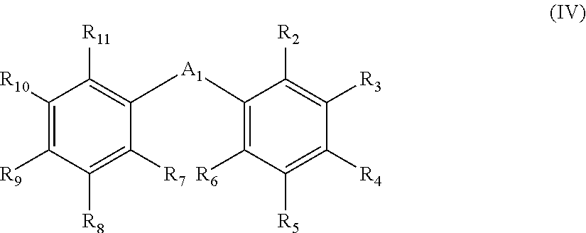
- R 2 , R 6 , R 7 and R 11 each independently represents a substituent
- R 3 , R 4 , R 5 , R 8 , R 9 and R 10 each independently represents a hydrogen atom or a substituent
- a 1 is as defined in formula (I).
- R 12 , R 13 , R 14 , R 15 , R 16 , R 17 , R 18 , R 19 , R 20 , R 21 , R 22 , R 23 , R 24 and R 25 each independently represents a hydrogen atom or a substituent
- a 1 is as defined in formula (I).
- a 1 in formulae (I) to (V) is a group selected from the group consisting of groups (a), (b), (c), (d), (e) and (h) among the compound group (I).
- a 1 in formulae (I) to (V) is a group (c) among the compound group (I).
- the light-emitting layer comprises at least one triplet light-emitting material.
- the at least one triplet light-emitting material contained in the light-emitting layer is a platinum complex or an iridium complex.
- the lowest excited triplet energy level T 1 of the compound represented by any of formulae (I) to (V) is from not lower than 65 kcal/mol (272.35 kJ/mol) to not higher than 95 kcal/mol (398.05 kJ/mol).
- a glass transition temperature Tg of the compound represented by any of formulae (I) to (V) is from not lower than 130° C. to not higher than 400° C.
- the compound represented by the formula (I), (II), (III), (IV) or (V) has the same meaning as the “compound of the invention”.
- the organic electroluminescent element having an organic layer containing the compound of the invention has the same meaning as the “element of the invention”.
- the substituent group A is defined as follows.
- substituent group A examples include alkyl groups (preferably a C 1 -C 30 , more preferably a C 1 -C 20 , particularly preferably a C 1 -C 10 alkyl group, e.g., methyl, ethyl, iso-propyl, tert-butyl, n-octyl, n-decyl, n-hexadecyl), cycloalkyl groups (preferably a C 3 -C 30 , more preferably a C 1 -C 20 , particularly preferably a C 3 -C 10 cycloalkyl group, e.g., cyclopropyl, cyclopentyl, cyclohexyl), alkenyl groups (preferably a C 2 -C 30 , more preferably a C 2 -C 20 , particularly preferably a C 2 -C 10 alkenyl group, e.g., vinyl, allyl, 2-butenyl,
- R 1 represents a substituent which is selected from the group consisting of the aforementioned substituent group A.
- the suffix m represents an integer of 2 or more.
- the suffix n represents an integer of 1 or more.
- a 1 represents a group selected from the group consisting of the aforementioned compound group (I). When m or n is 2 or more, the plurality of R 1 's or A 1 's may be the same or different.
- R 1 is preferably an alkyl group, cycloalkyl group, alkenyl group, alkynyl group, aryl group, amino group, alkoxy group, aryloxy group, heterocyclic oxy group, alkoxycarbonyl group, aryloxycarbonyl group, acyloxy group, acylamino group, alkoxycarbonylamino group, aryloxycarbonylamino group, sulfonylamino group, alkylthio group, arylthio group, heterocyclic thio group, hydrazino group or heterocyclic group, more preferably an alkyl group, cycloalkyl group, aryl group, heterocyclic group or amino group, even more preferably an alkyl group, cycloalkyl group, aryl group, heterocyclic group or amino group, still more preferably an aryl group, heterocyclic group or amino group.
- a 1 is preferably selected from the group consisting of the compounds (a), (b), (c), (d), (e), (h), (i), (j), (k), (l) and (m), more preferably (a), (b), (c), (d), (e) and (h), even more preferably (a), (c) and (d), most preferably (c) in the aforementioned compound group (I).
- the suffix m represents an integer of 2 or more, preferably from not smaller than 2 to not greater than 5, even more preferably 2 or 3.
- the suffix n represents an integer of 1 or more, preferably from not smaller than 1 to not greater than 4, even more preferably from not smaller than 1 to not greater than 3, still more preferably 1 or 2, most preferably 1.
- the formula (I) is preferably the formula (II) or (III).
- the formula (III) is preferably the formula (IV) or (V).
- Z 1 to Z 15 each independently represent an atomic group selected from the group consisting of carbon, nitrogen, oxygen, sulfur, silicon and phosphorus required to form an unsaturated 5-membered ring.
- the unsaturated 5-membered ring formed by Z 1 to Z 15 can be substituted, the unsaturated 5-membered ring may have substituents.
- the bonds constituting the unsaturated 5-membered ring each may be any of combinations of single bond and double bond.
- Z 1 to Z 15 are preferably formed by carbon, nitrogen, silicon, sulfur and oxygen, more preferably carbon, nitrogen and silicon, even more preferably carbon and nitrogen.
- Z 1 to Z 15 each are selected from the group consisting of carbon and nitrogen atoms and the unsaturated rings formed by Z 1 , Z 2 , Z 3 , Z 4 and Z 5 , Z 6 , Z 7 , Z 8 , Z 9 and Z 10 and Z 10 , Z 11 , Z 12 , Z 13 , Z 14 and Z 15 each represent a substituted or unsubstituted pyrazole ring, imidazole ring or triazole ring.
- the unsaturated ring may have substituents.
- the plurality of substituents may be connected to each other to form a condensed ring.
- the suffix p represents 0 or 1, preferably 0.
- a 1 is as defined in the formula (I), including its preferred range.
- Z 16 to Z 33 each independently represent an atomic group selected from the group consisting of carbon, nitrogen, oxygen, sulfur, silicon and phosphorus required to form an unsaturated 6-membered ring.
- the unsaturated 6-membered ring may have substituents.
- the bonds constituting the unsaturated 6-membered ring each may be any of combinations of single bond and double bond.
- Z 16 to Z 33 are preferably formed by carbon, nitrogen, silicon, sulfur and oxygen, more preferably carbon, nitrogen and silicon, even more preferably carbon and nitrogen.
- Z 16 to Z 33 each are selected from the group consisting of carbon and nitrogen atoms and the unsaturated rings formed by Z 16 , Z 17 , Z 18 , Z 19 , Z 20 and Z 21 and Z 22 , Z 23 , Z 24 , Z 25 , Z 26 and Z 27 and Z 28 , Z 29 , Z 30 , Z 31 , Z 32 and Z 33 each represent a substituted or unsubstituted benzene ring, pyridine ring, pyrazine ring, pyrimidine ring or pyridazine ring.
- the unsaturated ring may have substituents.
- the plurality of substituents may be connected to each other to form a condensed ring.
- the suffix q represents 0 or 1, preferably 0.
- a 1 is as defined in the formula (I), including its preferred range.
- R 2 , R 6 , R 7 and R 11 each represent a substituent and R 3 , R 4 , R 5 , R 8 , R 9 and R 10 each represent a hydrogen atom or substituent.
- the substituents represented by R 2 to R 11 each are selected from the group consisting of the aforementioned substituent group (A).
- R 2 , R 6 , R 7 and R 11 each are preferably an alkyl group, cycloalkyl group, alkenyl group, alkynyl group, aryl group, amino group, alkoxy group, aryloxy group, heterocyclic oxy group, alkylthio group, arylthio group, heterocyclic thio group, heterocyclic group, hydroxyl group, halogen atom or cyano group, more preferably an alkyl group, cycloalkyl group, aryl group, heterocyclic group or halogen atom, even more preferably an aryl group or heterocyclic group.
- R 3 , R 4 , R 5 , R 8 , R 9 and R 10 each are preferably a hydrogen atom, alkyl group, cycloalkyl group, alkenyl group, alkynyl group, aryl group, amino group, alkoxy group, aryloxy group, heterocyclic oxy group, alkylthio group, arylthio group, heterocyclic thio group, heterocyclic group, hydroxyl group, halogen atom or cyano group, more preferably a hydrogen atom, alkyl group, cycloalkyl group, aryl group, heterocyclic group or halogen atom, even more preferably a hydrogen atom, aryl group or heterocyclic group.
- R 2 to R 11 each represent a substituent, the plurality of substituents may be connected to each other to form a condensed ring.
- a 1 is as defined in the formula (I), including its preferred range.
- R 12 , R 13 , R 14 , R 15 , R 16 , R 17 , R 18 , R 19 , R 20 , R 21 , R 22 , R 23 , R 24 and R 25 each independently represents a hydrogen atom or a substituent; in case that R 12 , R 13 , R 14 , R 15 , R 16 , R 17 , R 18 , R 19 , R 20 , R 21 , R 22 , R 23 , R 24 and R 25 each independently represents a substituent, the substituent is selected from the aforementioned substituents group (A) and the substituent is preferably a hydrogen atom, alkyl group, cycloalkyl group, alkenyl group, alkynyl group, aryl group, alkoxy group, aryloxy group, heterocyclic oxy group, alkylthio group, arylthio group, heterocyclic thio group, heterocyclic thio group, heterocycl
- a 1 is as defined in the formula (I), including its preferred range.
- the lowest excited triplet energy level (hereinafter occasionally referred to as “T 1 ”) of the compound represented by any of the formulae (I) to (V) is preferably from not smaller than 65 kcal/mol (272.35 kJ/mol) to not greater than 95 kcal/mol (398.05 kJ/mol), more preferably from not smaller than 65 kcal/mol (272.35 kJ/mol) to not greater than 80 kcal/mol (335.2 kJ/mol), even more preferably from not smaller than 65 kcal/mol (272.35 kJ/mol) to not greater than 75 kcal/mol (314.3 kJ/mol), particularly preferably from not smaller than 65 kcal/mol (272.35 kJ/mol) to not greater than 70 kcal/mol (293.3 kJ/mol).
- the compound represented by any of the formulae (I) to (V) preferably exhibits a glass transition temperature (hereinafter abbreviated as “Tg”) of from not lower than 130° C. to not higher than 400° C., more preferably from not lower than 140° C. to 350° C., even more preferably from not lower than 150° C. to not higher than 300° C. from the standpoint of depositability, thermal stability, amorphism of film and inhibition of crystallization.
- Tg glass transition temperature
- the compound of the invention may be a low molecular compound or may be an oligomer compound or polymer compound (mass-average molecular weight (as calculated in terms of polystyrene): preferably from 1,000 to 5,000,000, more preferably from 2,000 to 1,000,000, even more preferably from 3,000 to 100,000).
- the compound of the invention is a polymer compound
- the structure represented by any of the formulae (I) to (V) may be incorporated in the polymer main chain or polymer side chains.
- the polymer compound as compound of the invention may be a homopolymer compound or copolymer.
- the compound of the invention is preferably a low molecular compound.
- the compound of the invention may be applied to organic EL elements and may be used as any of a light-emitting material, host material, exciton-blocking material, charge-blocking material or charge-transporting material, preferably a light-emitting material, host material, exciton-blocking material or charge-transporting material, more preferably a host material, exciton-blocking material or charge-transporting material, still more preferably a charge-transporting material.
- the light-emitting material may be ultraviolet-emitting, visible light-emitting or infrared-emitting or may be fluorescence or phosphorescence.
- the compound of the invention is to be contained as a light-emitting material in a light-emitting layer
- the compound of the invention is contained at preferably 0.5% by mass to 99.5% by mass, more preferably 1% by mass to 30% by mass, and particularly preferably 1% by mass to 10% by mass in the light-emitting layer.
- the compound of the invention is to be contained as a host material in a light-emitting layer
- the compound of the invention is contained at preferably 0.5% by mass to 99.5% by mass, more preferably 70% by mass to 99% by mass, and particularly preferably 90% by mass to 99% by mass in the light-emitting layer.
- the compound of the invention is to be contained in a layer except a light-emitting layer
- the compound of the invention is contained at preferably 1% by mass to 100% by mass, more preferably 5% by mass to 100% by mass, and particularly preferably 10% by mass to 100% by mass.
- the exemplified compound (1) in the inventive compounds represented by the formula (I) can be synthetically prepared according to Journal of the American Chemical Society, 57, 367-368, (1935); and the exemplified compound (41) therein can be synthetically prepared according to Tetrahedron, 24, 4285-4297, (1968)
- Exemplified compounds other than those described above may be synthetically prepared with reference to the methods described in Organometallics, 20, 418-423, (2001) and the like. But the methods for synthetic preparation thereof are not limited to the methods described herein.
- the reaction time during which the compound represented by any of the formulae (I) to (V) of the invention is synthesized depends on the reaction activity and thus is not specifically limited but is preferably from not shorter than 1 minute to not longer than 5 days, more preferably from not shorter than 5 minutes to not longer than 3 days, even more preferably from not shorter than 10 minutes to not longer than 24 hours.
- the compound (A) was synthesized according to “Bulletin of The Chemical Society of Japan 1999”, (72), 1, 115-120.
- Into a 200 mL three-necked flask were charged 3.40 g (7.83 mmol) of the compound (A) and 17 ml of ethanol.
- To the mixture which was being stirred at room temperature was then added 0.46 g (12 mmol) of sodium borohydride.
- the mixture was then heated under reflux with stirring for 2 hours.
- the reaction mixture was then allowed to cool to room temperature.
- To the reaction mixture was then added acetone.
- the reaction mixture was then stirred for 1 hour.
- To the reaction mixture was then added water.
- the resulting aqueous phase was then extracted with ethyl acetate.
- the organic phase thus collected was then dried over anhydrous magnesium sulfate.
- the resulting inorganic salt was withdrawn by filtration, and then concentrated by a rotary evaporator to quantitatively obtain 3.
- the resulting crude crystal was withdrawn by filtration, and then washed with water.
- the crude crystal thus obtained was heated under reflux with ethyl acetate so that it was completely dissolved in ethyl acetate, and then dried over anhydrous magnesium sulfate.
- the resulting inorganic salt was withdrawn by filtration, and then concentrated by a rotary evaporator.
- the residue thus obtained was then purified through silica gel chromatography to obtain 3.48 g (yield: 67.0%) of the compound (61) of the invention.
- the light-emitting element containing the compound of the invention will be further described hereinafter.
- the light-emitting element of the invention may be used for ordinary light-emitting systems, driving methods, etc. in ordinary embodiments except in that it is an element comprising the compound of the invention.
- the compound represented by any of the formulae (I) to (V) is preferably used as a light-emitting material, host material, exciton-blocking material, charge-blocking material or charge-transporting material, more preferably as a host material, exciton-blocking material or charge-transporting material.
- the light-emitting material may be ultraviolet-emitting or infrared-emitting or may be fluorescence or phosphorescence.
- the charge-transporting material may be positive hole-transporting or electron-transporting.
- a representative example of the light-emitting element is an organic EL (electroluminescent) element.
- organic electroluminescent element (hereinafter occasionally referred to as “organic EL element”) will be further described hereinafter.
- the light-emitting element of the invention comprises a cathode and an anode provided on a substrate and at least one organic layer (the organic layer may be a layer composed of only organic compounds, or may include inorganic compounds) containing at least an organic light-emitting layer (hereinafter occasionally referred to as “light-emitting layer”) provided interposed therebetween.
- the organic layer may be a layer composed of only organic compounds, or may include inorganic compounds
- at least an organic light-emitting layer hereinafter occasionally referred to as “light-emitting layer”
- At least one of the cathode and the anode is preferably transparent from the standpoint of the properties of light-emitting element.
- Glass if used as substrate, is preferably alkali-free glass to reduce the amount of ions eluted from glass.
- the shape, structure, size and other factors of the substrate are not specifically limited and can be properly predetermined depending on the use, purpose, etc. of the light-emitting element to be provided thereon.
- the shape of the substrate is preferably sheet-like.
- the substrate may have a single-layer structure or a laminated structure or may be formed by a single member or two or more members.
- the substrate may be colorless and transparent or colored and transparent but is preferably colorless and transparent to prevent scattering or damping of light emitted by the organic light-emitting layer.
- the substrate may have a moisture barrier layer (gas barrier layer) provided on one or the other side thereof.
- a moisture barrier layer gas barrier layer
- any anode may be normally used so far as it acts as an electrode capable of supplying positive holes to the organic layer.
- the shape, structure, size and other factors of the anode are not specifically limited.
- the anode can be properly selected from known electrode materials depending on the use and purpose of the light-emitting element.
- the anode is normally provided as a transparent anode.
- the position at which the anode is formed is not specifically limited and can be properly predetermined depending on the use and purpose of the light-emitting element but is preferably on the aforementioned substrate.
- the anode may be formed on the whole or part of one surface of the substrate.
- the thickness of the anode may be properly predetermined depending on the material constituting the anode and thus cannot be unequivocally predetermined but is normally from about 10 nm to 50 ⁇ m, preferably from 50 nm to 20 ⁇ m.
- the resistivity of the anode is preferably 10 3 ⁇ / ⁇ or less, more preferably 10 2 ⁇ / ⁇ or less.
- the anode is colorless or colored.
- the transmittance of the anode is preferably 60% or more, more preferably 70% or more.
- ITO or IZO is preferably subjected to film formation at a temperature as low as 150° C. or less to form a transparent anode.
- Examples of the material constituting the cathode include metals, alloys, metal oxides, electrically-conductive compounds, and mixtures thereof.
- Specific examples of the cathode material include alkaline metals (e.g., Li, Na, K, Cs), alkaline earth metals (e.g., Mg, Ca), gold, silver, lead, aluminum, sodium-potassium alloy, lithium-aluminum alloy, magnesium-silver alloy, indium, and rare earth metals such as ytterbium. These cathode materials may be used singly used. However, these cathode materials can be used in combination of two or more thereof to advantage from the standpoint of accomplishment of both stability and electron injecting properties.
- cathode materials are alkaline metals and alkaline rare earth metals from the standpoint of electron injecting properties or aluminum-based materials from the standpoint of storage stability.
- aluminum-based materials as used herein is meant to include aluminum in simple body, and alloy of mixture of aluminum with from 0.01% to 10% by mass of alkaline metal or alkaline earth metal (e.g., lithium-aluminum alloy, magnesium-aluminum alloy). (In this specification, mass ratio is equal to weight ratio.)
- the formation of the cathode is not specifically limited and can be accomplished by any known methods.
- the cathode can be formed according to a method which is properly selected from the group consisting of wet method such as printing method and coating method, physical method such as vacuum metallizing method, sputtering method and ion plating method and chemical method such as CVD method and plasma CVD method taking into account the adaptability to the material constituting the cathode. For example, when metals or the like are selected as cathode material, one or more of these materials can be simultaneously or successively sputtered or otherwise processed.
- the patterning for the formation of the cathode may be carried out by a chemical etching method involving photolithography or the like or a physical etching method involving laser or the like.
- a chemical etching method involving photolithography or the like or a physical etching method involving laser or the like.
- vacuum metallizing, sputtering or the like may be effected with a mask imposed on the substrate.
- patterning may be carried out by a lift-off method or printing method.
- the position at which the cathode is formed is not specifically limited.
- the cathode may be formed on the whole or part of the organic layer.
- a dielectric material layer made of a fluoride or oxide of alkaline metal or alkaline earth metal or the like may be provided interposed between the cathode and the organic layer to a thickness of from 0.1 nm to 5 nm.
- This dielectric material layer can be regarded also as an electron injecting layer.
- the dielectric layer can be formed by vacuum metallizing method, sputtering method, ion plating method or the like.
- the thickness of the cathode can be properly predetermined depending on the material constituting the cathode and thus cannot be unequivocally predetermined but is normally from about 10 nm to 5 ⁇ m, preferably from 50 nm to 1 ⁇ m.
- the cathode may be transparent or opaque.
- the transparent cathode can be formed by depositing a cathode material to a thickness as small as from 1 nm to 10 nm, and then laminating a transparent electrically-conductive material such as ITO and IZO on the thin film.
- the organic electroluminescent element of the invention comprises at least one organic layer containing a light-emitting layer.
- organic layers other than organic light-emitting layer include various layers such as positive hole-transporting layer, electron-transporting layer, charge-blocking layer, positive hole-injecting layer and electron-injecting layer.
- the various layers constituting the organic layer can be fairly formed by any of dry film-forming method such as vacuum metallizing method and sputtering method, transfer method and printing method.
- the organic light-emitting layer is a layer capable of receiving positive holes from the anode, the positive hole-injecting layer or the positive hole-transporting layer and electrons from the cathode, the electron-injecting layer or the electron-transporting layer during the application of an electric field to provide a site for the recombination of positive holes with electrons, causing light emission.
- the light-emitting layer in the invention may be formed by a light-emitting material alone or a host material and a light-emitting material in admixture.
- the light-emitting material may be a fluorescent material or a phosphorescent material.
- One or more dopants may be used.
- the host material may be a charge-transporting material.
- One or more host materials may be used. For example, an electron-transporting host material and a hole-transporting host material may be used in admixture.
- the light-emitting layer may further contains a material which neither has charge-transporting properties nor emits light.
- the light-emitting layer may consist of one or more layers which may emit lights having different colors, respectively.
- Examples of the fluorescent material which can be used in combination with the compound represented by the formula (I) of the invention include benzooxazole derivatives, benzoimidazole derivatives, benzothiazole derivatives, styrylbetzene derivatives, polyphenyl derivatives, diphenylbutadiene derivatives, tetraphenylbutadiene derivatives, naphthalimide derivatives, coumarine derivatives, condensed aromatic compounds, perynone derivatives, oxadiazole derivatives, oxazine derivatives, aldazine derivatives, pyralidine derivatives, cyclopentadiene derivatives, bisstyrylanthracene derivatives, quinacridone derivatives, pyrrolopyridine derivatives, thiadiazopyridine derivatives, cyclopentadiene derivatives, styrylamine derivatives, diketopyrrolopyrole derivatives, aromatic dimethylidine compounds, various metal complexes such as metal complex of
- ligands to be incorporated in these complexes include those disclosed in G. Wilkinson et al, “Comprehensive Coordination Chemistry”, Pergamon Press, 1987, H. Yersin, “Photochemistry and Photophysics of Coordination Compounds”, Springer-Verlag, 1987, Akio Yamomoto, “Yukikinzokukagaku-Kiso to Oyo-(Organic Metal Chemistry—Basic Study and Application)”, Shokabo, 1982, etc.
- the ligands include halogen ligands (preferably chlorine ligands), nitrogen-containing heterocyclic ligands (preferably phenylpyridine, benzoquinoline, quinolyl, bipyridyl, phenanthroline, etc.), diketone ligands (e.g., acetylacetone), carboxylic acid ligands (e.g., acetic acid ligand), carbon monoxide ligand, isonitrile ligand, and cyano ligand. More desirable among these ligands are nitrogen-containing heterocyclic ligands.
- the aforementioned complex may have one transition metal atom incorporated therein or may be a so-called binuclear complex having two or more transition metal atoms incorporated therein. The complex may have different metal atoms incorporated therein at the same time.
- the phosphorescent material may be incorporated in the light-emitting layer in an amount of from 0.1% to 40% by mass, more preferably from 0.5% to 20% by mass.
- the phosphorescent material is preferably a platinum complex or an iridium complex, more preferably a platinum complex.
- the platinum complex described in WO 2004/108857 is more preferable.
- Examples of the host material to be incorporated in the light-emitting layer of the invention include those having a carbazole skeleton, those having a diarylamine skeleton, those having a pyridine skeleton, those having a pyrazine skeleton, those having a triazine skeleton, those having a arylsilane skeleton, and materials exemplified later with reference to positive hole-injecting layer, positive hole-transporting layer, electron-injecting layer and electron-transporting layer.
- the thickness of the light-emitting layer is not specifically limited but is normally preferably from 1 nm to 500 nm, more preferably from 5 nm to 200 nm, even more preferably from 10 nm to 100 nm.
- the positive hole-injecting layer and the positive hole-transporting layer each are a layer capable of receiving positive holes from the anode or anode side and then transporting them to the cathode side.
- the positive hole-injecting layer and the positive hole-transporting layer each preferably are a layer containing a carbazole derivative, triazole derivative, oxazole derivative, oxadiazole derivative, imidazole derivative, polyarylalkane derivative, pyrazoline derivative, pyrazolone derivative, phenylenediamine derivative, arylamine derivative, amino-substituted chalcone derivative, styrylanthracene derivative, fluorenone derivative, hydrazone derivative, stilbene derivative, silazalane derivative, aromatic tertiary amine compound, styrylamine compound, aromatic dimethylidene-based compound, porphiline-based compound, organic silane derivative, carbon or the like.
- the thickness of the positive hole-injecting layer and the positive hole-transporting layer each preferably are 500 nm or less to lower the required driving voltage.
- the thickness of the positive hole-transporting layer is preferably from 1 nm to 500 nm, more preferably from 5 nm to 200 nm, even more preferably from 10 nm to 100 nm.
- the thickness of the positive hole-injecting layer is preferably from 0.1 nm to 200 nm, more preferably from 0.5 nm to 100 nm, even more preferably from 1 nm to 100 nm.
- the positive hole-injecting layer and the positive hole-transporting layer each may be a single layer structure composed of one or more of the aforementioned materials or a multi-layer structure composed of a plurality of layers having the same or different compositions.
- Electron-Injecting Layer Electron-Transporting Layer
- the electron-injecting layer and the electron-transporting layer each are a layer capable of receiving electrons from the cathode or anode and then transporting them to the anode side.
- the electron-injecting and the electron-transporting layer each preferably are a layer containing a triazole derivative, oxazole derivative, oxadiazole derivative, imidazole derivative, fluorenone derivative, anthraquinodimethane derivative, anthrone derivative, diphenylquinone derivative, thiopyrandioxide derivative, carbodiimide derivative, fluorenylidenemethane derivative, distyrylpyrazine derivative, naphthalene and aromatic tetracarboxylic anhydride, phthalocyanine derivative, various metal complexes such as metal complex of 8-quinolyl derivative and metal complex having metal phthalocyanine, benzooxazole or benzothiazole as ligand, organic silane derivative or the like.
- the thickness of the electron-injecting layer and the electron-transporting layer each are preferably 50 nm or less to lower the required driving voltage.
- the thickness of the electron-transporting layer is preferably from 1 nm to 500 nm, more preferably from 5 nm to 200 nm, even more preferably from 10 nm to 100 nm.
- the thickness of the electron-transporting layer is preferably from 0.1 nm to 200 nm, more preferably from 0.2 nm to 100 nm, even more preferably from 0.5 nm to 50 nm.
- the electron-injecting layer and the electron-transporting layer each may be a single layer structure composed of one or more of the aforementioned materials or a multi-layer structure composed of a plurality of layers having the same or different compositions.
- the positive hole-blocking layer is a layer capable of preventing positive holes which have been transported from the anode side to the light-emitting layer from passing to the cathode side.
- a positive hole-blocking layer may be provided as an organic layer-adjacent to the light-emitting layer on the cathode side thereof.
- organic compound constituting the positive hole-blocking layer examples include aluminum complexes such as BAlq, triazole derivatives, and phenanthroline derivatives such as BCP.
- the thickness of the positive hole-blocking layer is preferably from 1 nm to 500 nm, more preferably from 5 nm to 200 nm, even more preferably from 10 nm to 100 nm.
- the positive hole-blocking layer may be a single layer structure composed of one or more of the aforementioned materials or a multi-layer structure composed of a plurality of layers having the same or different compositions.
- the organic EL element may be entirely protected by a protective layer.
- the materials to be incorporated in the protective layer may be any materials capable of preventing materials which accelerate the deterioration of the element such as water content and oxygen from entering in the element.
- the materials to be incorporated in the protective layer include metals such as In, Sn, Pb, Au, Cu, Ag, Al, Ti and Ni, metal oxides such as MgO, SiO, SiO 2 , Al 2 O 3 , GeO, NiO, CaO, BaO, Fe 2 O 3 , Y 2 O 3 and TiO 2 , metal nitrides such as SiN x and SiN x O y , metal fluorides such as MgF 2 , LiF, AlF 3 and CaF 2 , polyethylenes, polypropylenes, polymethyl methacrylates, polyimides, polyureas, polytetrafluoroethylenes, polychloro trifluoroethylenes, polydicblorodifluoroethylene, copolymers of chlorotrifluoroethylene with dichlorodifluoroethylene, copolymers obtained by the copolymerizatin of tetrafluoroethylene with a monomer mixture containing at least one comonomer,
- the method for forming the protective layer is not specifically limited.
- vacuum metallizing method sputtering method, reactive sputtering method, MBE (Molecular Beam Epitaxy) method, cluster-ion beam method, ion plating method, plasma polymerization method (high frequency excited ion plating method), plasma CVD method, laser CVD method, hot CVD method, gas source CVD method, coating method, printing method or transfer method may be applied.
- the organic electroluminescent element of the invention may be entirely encapsulated using an encapsulating vessel.
- the space between the encapsulating vessel and the light-emitting element may be filled with a water absorber or an inert liquid.
- the water absorbing agent is not specifically limited.
- Examples of the water absorbing agent employable herein include barium oxide, sodium oxide, potassium oxide, calcium oxide, sodium sulfate, calcium sulfate, magnesium sulfate, phosphorus pentaoxide, calcium chloride, magnesium chloride, copper chloride, cesium fluoride, niobium fluoride, calcium bromide, vanadium bromide, molecular sieve, zeolite, and magnesium oxide.
- the inert liquid is not specifically limited. Examples of the inert liquid employable herein include paraffins, liquid paraffins, fluorine-based solvents such as perfluoroalkane, perfluoroamine and perfluoroether, chlorine-based solvents, and silicone oils.
- the organic electroluminescent element of the invention can emit light when dc voltage (normally from 2 volt to 15 volt, optionally including ac components) is applied across the anode and the cathode or dc current is allowed to flow from the anode to the cathode.
- dc voltage normally from 2 volt to 15 volt, optionally including ac components
- JP-A-2-148687, JP-A-6-301355, JP-A-5-29080, JP-A-7-134558, JP-A-8-234685, JP-A-8-241047, Japanese Patent Application No. 2784615, and U.S. Pat. Nos. 5,828,429 and 6,023,308 may be applied.
- a substrate with a rinsed ITO electrodeposition layer was placed in a vapor deposition apparatus, onto which NPD was vapor-deposited to 50 nm.
- CBP and Compound (79) (a compound described in WO 2004/108857) were additionally vapor-deposited at a mass ratio of 10:1 thereon to 40 nm, onto which BAlq was vapor-deposited to 3 nm.
- BAlq was vapor-deposited to 3 nm.
- Alq was vapor-deposited thereon to 30 nm.
- a patterned musk (to a luminescent area of 4 mm+5 mm) was mounted on the resulting organic film, followed by 3-nm vapor deposition of lithium fluoride and subsequent 60-nm vapor deposition of aluminium, to prepare the organic EL element of Comparative Example 1.
- the organic EL element of Example 1 was prepared.
- a DC constant current passed through the resulting organic EL element at a current density of 500 A/m 2 , luminescence could be observed.
- the driving voltage then was 12.0 V.
- the driving voltage was increased to 13.5 V via 10-hour luminescence at a brightness of 300 cd/m 2 .
- the increment of the driving voltage was small, compared with Comparative Example 1.
- a light-emitting element having a low required driving voltage can be provided.
- the organic electroluminescent element of the invention can be used in the art of display element, display, backlight, electrophotography, illumination light source, recording light source, exposure light source, reading light source, sign, signboard, interior, optical communication, etc.
- the compound of the invention can be applied also to medical use, fluorescent brightening agent, photographic material, UV-absorbing material, laser dye, recording media material, ink jet pigment, color filter dye, color conversion filter, analysis, etc.
Landscapes
- Chemical & Material Sciences (AREA)
- Engineering & Computer Science (AREA)
- Materials Engineering (AREA)
- Organic Chemistry (AREA)
- Physics & Mathematics (AREA)
- Spectroscopy & Molecular Physics (AREA)
- Electroluminescent Light Sources (AREA)
Abstract
Description
(R1)m-(A1)n (I)
Compound group (I):


<Synthesis of Compound (52) of the Invention>

Claims (13)


Applications Claiming Priority (3)
| Application Number | Priority Date | Filing Date | Title |
|---|---|---|---|
| JP2005291145 | 2005-10-04 | ||
| JP2005-291145 | 2005-10-04 | ||
| JPP.2005-291145 | 2005-10-04 |
Publications (2)
| Publication Number | Publication Date |
|---|---|
| US20070077453A1 US20070077453A1 (en) | 2007-04-05 |
| US8206839B2 true US8206839B2 (en) | 2012-06-26 |
Family
ID=37951934
Family Applications (1)
| Application Number | Title | Priority Date | Filing Date |
|---|---|---|---|
| US11/542,550 Active 2029-05-08 US8206839B2 (en) | 2005-10-04 | 2006-10-04 | Organic electroluminescent element |
Country Status (1)
| Country | Link |
|---|---|
| US (1) | US8206839B2 (en) |
Cited By (1)
| Publication number | Priority date | Publication date | Assignee | Title |
|---|---|---|---|---|
| US20110140043A1 (en) * | 2008-07-18 | 2011-06-16 | Merck Patent Gmbh | Materials for organic electroluminescence device |
Families Citing this family (11)
| Publication number | Priority date | Publication date | Assignee | Title |
|---|---|---|---|---|
| WO2010018858A1 (en) * | 2008-08-13 | 2010-02-18 | 財団法人山形県産業技術振興機構 | Organic sulfur compound, process for production of the same, and organic electroluminescence element utilizing the same |
| KR20100054110A (en) * | 2008-11-13 | 2010-05-24 | 주식회사 엘지화학 | Organic light emitting diode having low operating voltage and method for fabricating the same |
| DE102009014513A1 (en) * | 2009-03-23 | 2010-09-30 | Merck Patent Gmbh | Organic electroluminescent device |
| CN106025099B (en) | 2011-04-12 | 2018-09-07 | 精工爱普生株式会社 | Light-emitting component, light-emitting device, authentication device and electronic equipment |
| JP5765034B2 (en) | 2011-04-18 | 2015-08-19 | セイコーエプソン株式会社 | Thiadiazole compounds, compounds for light emitting devices, light emitting devices, light emitting devices, authentication devices, and electronic devices |
| JP5790279B2 (en) * | 2011-08-09 | 2015-10-07 | セイコーエプソン株式会社 | LIGHT EMITTING ELEMENT, LIGHT EMITTING DEVICE, AND ELECTRONIC DEVICE |
| KR20130018547A (en) | 2011-08-09 | 2013-02-25 | 세이코 엡슨 가부시키가이샤 | Thiadiazole, light-emitting element, light-emitting apparatus, authentication apparatus, and electronic device |
| JP5970811B2 (en) | 2011-12-28 | 2016-08-17 | セイコーエプソン株式会社 | LIGHT EMITTING ELEMENT, LIGHT EMITTING DEVICE, AND ELECTRONIC DEVICE |
| US9324952B2 (en) | 2012-02-28 | 2016-04-26 | Seiko Epson Corporation | Thiadiazole, compound for light-emitting elements, light-emitting element, light-emitting apparatus, authentication apparatus, and electronic device |
| US9722184B2 (en) | 2012-10-18 | 2017-08-01 | Seiko Epson Corporation | Thiadiazole, compound for light-emitting elements, light-emitting element, light-emitting apparatus, authentication apparatus, and electronic device |
| CN104961758A (en) * | 2015-07-22 | 2015-10-07 | 中国烟草总公司郑州烟草研究院 | Chain musk odorant and preparation method thereof |
Citations (18)
| Publication number | Priority date | Publication date | Assignee | Title |
|---|---|---|---|---|
| JPH08143862A (en) | 1994-11-25 | 1996-06-04 | Toray Ind Inc | Light emitting element |
| US6008299A (en) * | 1997-08-15 | 1999-12-28 | Innotech, Inc., Johnson & Johnson Vision Care | Optic devices formed from melt processable thermoplastic materials having a high refractive index |
| JP2002063989A (en) | 2000-06-08 | 2002-02-28 | Toray Ind Inc | Light emitting element |
| US20020028329A1 (en) * | 2000-07-17 | 2002-03-07 | Fuji Photo Film Co., Ltd. | Light emitting element and azole compound |
| US6416887B1 (en) * | 1998-11-11 | 2002-07-09 | Kabushiki Kaisha Toyota Chuo Kenkyusho | Organic electroluminescent element |
| US20030181694A1 (en) * | 2001-06-25 | 2003-09-25 | Koro Shirane | Light-emitting material and organic light-emitting device |
| JP2003317965A (en) | 2002-04-25 | 2003-11-07 | Konica Minolta Holdings Inc | Organic electroluminescence element and display device |
| JP2004095221A (en) | 2002-08-29 | 2004-03-25 | Toray Ind Inc | Light emitting element |
| WO2004093207A2 (en) | 2003-04-15 | 2004-10-28 | Covion Organic Semiconductors Gmbh | Mixtures of matrix materials and organic semiconductors capable of emission, use of the same and electronic components containing said mixtures |
| WO2004108857A1 (en) | 2003-06-02 | 2004-12-16 | Fuji Photo Film Co., Ltd. | Organic electroluminescent devices and metal complex compounds |
| US20040265624A1 (en) * | 2002-12-19 | 2004-12-30 | Satoko Shitagaki | Organic lighting emitting element, organic lighting emitting device having the organic lighting emitting element, and electronic appliance having the organic lighting emitting device |
| WO2005003253A2 (en) | 2003-07-07 | 2005-01-13 | Covion Organic Semiconductors Gmbh | Mixtures of organic emissive semiconductors and matrix materials, their use and electronic components comprising said materials |
| WO2005017065A1 (en) * | 2003-08-19 | 2005-02-24 | Covion Organic Semiconductors Gmbh | Oligomer and polymer comprising triphenyl phosphine units |
| WO2005042444A2 (en) | 2003-11-04 | 2005-05-12 | Takasago Perfumery Co Ltd | Platinum complex and luminescent element |
| WO2005042550A1 (en) | 2003-10-30 | 2005-05-12 | Merck Patent Gmbh | Metal complexes with bipodal ligands |
| WO2005054403A1 (en) | 2003-12-05 | 2005-06-16 | Merck Patent Gmbh | Organic electroluminescent element |
| WO2005084082A1 (en) | 2004-02-20 | 2005-09-09 | Merck Patent Gmbh | Organic electronic devices |
| WO2006000388A1 (en) | 2004-06-26 | 2006-01-05 | Merck Patent Gmbh | Organic electroluminescent device |
-
2006
- 2006-10-04 US US11/542,550 patent/US8206839B2/en active Active
Patent Citations (23)
| Publication number | Priority date | Publication date | Assignee | Title |
|---|---|---|---|---|
| JPH08143862A (en) | 1994-11-25 | 1996-06-04 | Toray Ind Inc | Light emitting element |
| US6008299A (en) * | 1997-08-15 | 1999-12-28 | Innotech, Inc., Johnson & Johnson Vision Care | Optic devices formed from melt processable thermoplastic materials having a high refractive index |
| US6416887B1 (en) * | 1998-11-11 | 2002-07-09 | Kabushiki Kaisha Toyota Chuo Kenkyusho | Organic electroluminescent element |
| JP2002063989A (en) | 2000-06-08 | 2002-02-28 | Toray Ind Inc | Light emitting element |
| US20020028329A1 (en) * | 2000-07-17 | 2002-03-07 | Fuji Photo Film Co., Ltd. | Light emitting element and azole compound |
| US20030181694A1 (en) * | 2001-06-25 | 2003-09-25 | Koro Shirane | Light-emitting material and organic light-emitting device |
| JP2003317965A (en) | 2002-04-25 | 2003-11-07 | Konica Minolta Holdings Inc | Organic electroluminescence element and display device |
| JP2004095221A (en) | 2002-08-29 | 2004-03-25 | Toray Ind Inc | Light emitting element |
| US20040265624A1 (en) * | 2002-12-19 | 2004-12-30 | Satoko Shitagaki | Organic lighting emitting element, organic lighting emitting device having the organic lighting emitting element, and electronic appliance having the organic lighting emitting device |
| WO2004093207A2 (en) | 2003-04-15 | 2004-10-28 | Covion Organic Semiconductors Gmbh | Mixtures of matrix materials and organic semiconductors capable of emission, use of the same and electronic components containing said mixtures |
| WO2004108857A1 (en) | 2003-06-02 | 2004-12-16 | Fuji Photo Film Co., Ltd. | Organic electroluminescent devices and metal complex compounds |
| US20060255332A1 (en) | 2003-07-07 | 2006-11-16 | Heinrich Becker | Mixtures of organic emissive semiconductors and matrix materials, their use and electronic components comprising said materials |
| WO2005003253A2 (en) | 2003-07-07 | 2005-01-13 | Covion Organic Semiconductors Gmbh | Mixtures of organic emissive semiconductors and matrix materials, their use and electronic components comprising said materials |
| WO2005017065A1 (en) * | 2003-08-19 | 2005-02-24 | Covion Organic Semiconductors Gmbh | Oligomer and polymer comprising triphenyl phosphine units |
| US20070031698A1 (en) * | 2003-08-19 | 2007-02-08 | Covion Organic Semiconductors Gmbh | Oligomer and polymer comprising triphenyl phosphine units |
| WO2005042550A1 (en) | 2003-10-30 | 2005-05-12 | Merck Patent Gmbh | Metal complexes with bipodal ligands |
| WO2005042444A2 (en) | 2003-11-04 | 2005-05-12 | Takasago Perfumery Co Ltd | Platinum complex and luminescent element |
| WO2005054403A1 (en) | 2003-12-05 | 2005-06-16 | Merck Patent Gmbh | Organic electroluminescent element |
| WO2005084081A1 (en) | 2004-02-20 | 2005-09-09 | Merck Patent Gmbh | Organic electronic devices |
| WO2005084082A1 (en) | 2004-02-20 | 2005-09-09 | Merck Patent Gmbh | Organic electronic devices |
| US20070164273A1 (en) * | 2004-02-20 | 2007-07-19 | Merck Patent Gmbh | Organic electronic devices |
| US20070170419A1 (en) | 2004-02-20 | 2007-07-26 | Anja Gerhard | Organic electronic devices |
| WO2006000388A1 (en) | 2004-06-26 | 2006-01-05 | Merck Patent Gmbh | Organic electroluminescent device |
Non-Patent Citations (3)
| Title |
|---|
| Dedinas, J.; Regan, T. H. J. Phys. Chem. 76 (1972) 3926-3933. * |
| Office Action issued on Mar. 6, 2012 by the Japanese Patent Office in the corresponding Japanese Patent Application No. 2006-271604. |
| Yasuhiro Yamaguchi et al., "Nonadiabatic small-polaron hopping electron transport in diphenoquinone-doped polycarbonate" (1991), J. Appl. Phys., vol. 70, No. 1, pp. 3726-3729. |
Cited By (1)
| Publication number | Priority date | Publication date | Assignee | Title |
|---|---|---|---|---|
| US20110140043A1 (en) * | 2008-07-18 | 2011-06-16 | Merck Patent Gmbh | Materials for organic electroluminescence device |
Also Published As
| Publication number | Publication date |
|---|---|
| US20070077453A1 (en) | 2007-04-05 |
Similar Documents
| Publication | Publication Date | Title |
|---|---|---|
| US12402218B2 (en) | Organic electroluminescent device | |
| JP4399429B2 (en) | Organic electroluminescence device | |
| JP4789556B2 (en) | Organic electroluminescence device | |
| JP4399382B2 (en) | Organic electroluminescence device | |
| JP5144034B2 (en) | Organic electroluminescence device | |
| JP4945156B2 (en) | Organic electroluminescence device | |
| JP4934346B2 (en) | Organic electroluminescence device | |
| JP3963811B2 (en) | Organic electroluminescence device | |
| US8273467B2 (en) | Organic electroluminescent device | |
| JP4871607B2 (en) | Organic electroluminescence device | |
| JP2007266598A (en) | Organic electroluminescence device | |
| US8206839B2 (en) | Organic electroluminescent element | |
| JP3949391B2 (en) | Light emitting element | |
| JP4708749B2 (en) | ORGANIC ELECTROLUMINESCENT ELEMENT, AZEPINE COMPOUND AND METHOD FOR PRODUCING SAME | |
| JP2009004491A (en) | Organic electroluminescence device | |
| JP2006086482A (en) | Organic electroluminescence element | |
| JP4848198B2 (en) | Organic electroluminescence device | |
| JP5080774B2 (en) | Organic electroluminescence device | |
| JP2005222794A (en) | Organic electroluminescent device and method for preparing organic electroluminescent device material | |
| JP4849812B2 (en) | Organic electroluminescent device and silicon compound | |
| JP2007194506A (en) | Organic electroluminescence device | |
| JP5496748B2 (en) | Triphenylene compound | |
| JP2007194504A (en) | Organic electroluminescence device | |
| JP2006332116A (en) | Organic electroluminescence device | |
| JP2013062513A (en) | Organic electroluminescent element |
Legal Events
| Date | Code | Title | Description |
|---|---|---|---|
| AS | Assignment |
Owner name: FUJIFILM CORPORATION, JAPAN Free format text: ASSIGNMENT OF ASSIGNORS INTEREST;ASSIGNORS:SANO, SATOSHI;IGARASHI, TATSUYA;REEL/FRAME:018384/0503 Effective date: 20061002 |
|
| STCF | Information on status: patent grant |
Free format text: PATENTED CASE |
|
| AS | Assignment |
Owner name: UDC IRELAND LIMITED, IRELAND Free format text: ASSIGNMENT OF ASSIGNORS INTEREST;ASSIGNOR:FUJIFILM CORPORATION;REEL/FRAME:028889/0636 Effective date: 20120726 |
|
| FPAY | Fee payment |
Year of fee payment: 4 |
|
| MAFP | Maintenance fee payment |
Free format text: PAYMENT OF MAINTENANCE FEE, 8TH YEAR, LARGE ENTITY (ORIGINAL EVENT CODE: M1552); ENTITY STATUS OF PATENT OWNER: LARGE ENTITY Year of fee payment: 8 |
|
| MAFP | Maintenance fee payment |
Free format text: PAYMENT OF MAINTENANCE FEE, 12TH YEAR, LARGE ENTITY (ORIGINAL EVENT CODE: M1553); ENTITY STATUS OF PATENT OWNER: LARGE ENTITY Year of fee payment: 12 |