US8203380B2 - Semiconductor device - Google Patents
Semiconductor device Download PDFInfo
- Publication number
- US8203380B2 US8203380B2 US12/483,668 US48366809A US8203380B2 US 8203380 B2 US8203380 B2 US 8203380B2 US 48366809 A US48366809 A US 48366809A US 8203380 B2 US8203380 B2 US 8203380B2
- Authority
- US
- United States
- Prior art keywords
- low
- side switch
- semiconductor substrate
- driver
- switch
- Prior art date
- Legal status (The legal status is an assumption and is not a legal conclusion. Google has not performed a legal analysis and makes no representation as to the accuracy of the status listed.)
- Expired - Fee Related, expires
Links
Images


Classifications
-
- H—ELECTRICITY
- H02—GENERATION; CONVERSION OR DISTRIBUTION OF ELECTRIC POWER
- H02M—APPARATUS FOR CONVERSION BETWEEN AC AND AC, BETWEEN AC AND DC, OR BETWEEN DC AND DC, AND FOR USE WITH MAINS OR SIMILAR POWER SUPPLY SYSTEMS; CONVERSION OF DC OR AC INPUT POWER INTO SURGE OUTPUT POWER; CONTROL OR REGULATION THEREOF
- H02M7/00—Conversion of AC power input into DC power output; Conversion of DC power input into AC power output
- H02M7/003—Constructional details, e.g. physical layout, assembly, wiring or busbar connections
-
- H—ELECTRICITY
- H10—SEMICONDUCTOR DEVICES; ELECTRIC SOLID-STATE DEVICES NOT OTHERWISE PROVIDED FOR
- H10D—INORGANIC ELECTRIC SEMICONDUCTOR DEVICES
- H10D84/00—Integrated devices formed in or on semiconductor substrates that comprise only semiconducting layers, e.g. on Si wafers or on GaAs-on-Si wafers
- H10D84/80—Integrated devices formed in or on semiconductor substrates that comprise only semiconducting layers, e.g. on Si wafers or on GaAs-on-Si wafers characterised by the integration of at least one component covered by groups H10D12/00 or H10D30/00, e.g. integration of IGFETs
- H10D84/811—Combinations of field-effect devices and one or more diodes, capacitors or resistors
- H10D84/813—Combinations of field-effect devices and capacitor only
-
- H—ELECTRICITY
- H03—ELECTRONIC CIRCUITRY
- H03K—PULSE TECHNIQUE
- H03K2217/00—Indexing scheme related to electronic switching or gating, i.e. not by contact-making or -breaking covered by H03K17/00
- H03K2217/0081—Power supply means, e.g. to the switch driver
-
- H—ELECTRICITY
- H10—SEMICONDUCTOR DEVICES; ELECTRIC SOLID-STATE DEVICES NOT OTHERWISE PROVIDED FOR
- H10D—INORGANIC ELECTRIC SEMICONDUCTOR DEVICES
- H10D84/00—Integrated devices formed in or on semiconductor substrates that comprise only semiconducting layers, e.g. on Si wafers or on GaAs-on-Si wafers
- H10D84/80—Integrated devices formed in or on semiconductor substrates that comprise only semiconducting layers, e.g. on Si wafers or on GaAs-on-Si wafers characterised by the integration of at least one component covered by groups H10D12/00 or H10D30/00, e.g. integration of IGFETs
- H10D84/811—Combinations of field-effect devices and one or more diodes, capacitors or resistors
Definitions
- the present invention relates to a semiconductor device used for a power converter such as a power supply. More particularly, the present invention relates to a technique effectively applied to a non-isolated DC-DC converter.
- a power supply by a synchronous rectification method has been used so often with the achievement of low voltage driving of a power supply used for a CPU (Central Processing Unit) such as a computer.
- the current slew rate (di/dt) required for the CPU power supply has been increasing more and more, and therefore, the development of a higher-speed power supply has been important for suppressing ripple of an output voltage of the power supply.
- FIG. 1 shows a circuit diagram of a general non-isolated DC-DC converter for converting a direct-current voltage.
- An input capacitor Cin is arranged in parallel with an input power supply Vin.
- a drive capacitor Cdrive is inserted in parallel with a drive power supply Vdrive for driving a high-side switch Q 1 and a low-side switch Q 2 , thereby supplying power to a low-side driver 33 .
- a driver circuit for the high-side switch Q 1 has a boot strap configuration, and when the high-side switch Q 1 is turned off, current is supplied from the drive power supply Vdrive to a boot strap capacitor Cboot via a boot strap diode Dboot, thereby becoming a power supply for a high-side driver 32 .
- the high-side switch Q 1 and the low-side switch Q 2 are alternately turned on and off by receiving a PWM signal from a power supply controller 31 , so that square waves are outputted to a terminal Vx and the square waves are smoothed to a direct-current voltage by an output filter configured with an output inductor L and an output capacitor Cout, thereby supplying power to a CPU 34 to be a load.
- Diodes D 1 and D 2 are connected in antiparallel to the high-side switch Q 1 and the low-side switch Q 2 , respectively, and the diode D 1 assumes a role of ensuring a current path to the input power supply Vin when a potential of the Vx to be one terminal of the output inductor L is increased.
- the diode D 2 assumes a role of ensuring a return current path of the output inductor L when the high-side switch Q 1 is turned off.
- the synchronous rectification means an operation that the low-side switch Q 2 is turned on to switch the current path from the diode D 2 to the low-side switch Q 2 when the return current flows in the diode D 2 , and this can reduce the conduction loss because on-resistance of the low-side switch Q 2 is significantly low compared to the diode D 2 .
- a MOSFET Metal Oxide Semiconductor Field Effect Transistor
- a discrete package power MOSFET is used as the high-side switch Q 1 and the low-side switch Q 2 of a non-isolated DC-DC converter
- a driver IC including the high-side driver 32 and the low-side driver 33 for driving these switches is provided in a different package from the discrete package, and the switches are connected to the drivers on a printed board, respectively.
- the high-side driver 32 and the low-side driver 33 are arranged in a center region of the semiconductor substrate in a conventional structure disclosed in the above-described Patent Document 1 and the like, and therefore, there is a problem of path lengths among the input capacitor Cin, the drive capacitor Cdrive, and the boot strap capacitor Cboot, which are arranged so as to surround the semiconductor device.
- a path from a positive terminal of the input capacitor Cin to a negative terminal of the input capacitor Cin via the high-side switch Q 1 and the low-side switch Q 2 is long
- a path from a positive terminal of the drive capacitor Cdrive to a negative terminal of the drive capacitor Cdrive via the low-side driver 33 of the low-side switch Q 2 is long
- a path from a positive terminal of the boot strap capacitor Cboot to a negative terminal of the boot strap capacitor Cboot via the high-side driver 32 of the high-side switch Q 1 is long, and therefore, there are problems of the large parasitic inductance and the low conversion efficiency.
- an object of the present invention is to provide a semiconductor device of non-isolated DC-DC converter which has the reduced parasitic inductance and the high conversion efficiency.
- a semiconductor device includes a high-side switch, a high-side driver, a low-side switch, and a low-side driver, which are formed on the same semiconductor substrate, wherein the high-side driver is arranged in a region closer to a periphery of a semiconductor substrate than the high-side switch, and the low-side driver is arranged in a region closer to the periphery of the semiconductor substrate than the low-side switch.
- the high-side driver is arranged in each of regions closer to the periphery of the semiconductor substrate and the center of the semiconductor substrate than the high-side switch
- the low-side driver is arranged in each of regions closer to the periphery of the semiconductor substrate and the center of the semiconductor substrate than the low-side switch.
- the high-side driver is arranged in a region closer to the periphery of the semiconductor substrate than the high-side switch, and the low-side driver is arranged in a region closer to the periphery of the semiconductor substrate than the high-side switch.
- a path from a positive terminal of the input capacitor to a negative terminal of the input capacitor via the high-side switch and the low-side switch is short
- a path from a positive terminal of the drive capacitor to a negative terminal of the drive capacitor via the low-side driver of the low-side switch is short
- a path from a positive terminal of the boot strap capacitor to a negative terminal of the boot strap capacitor via the high-side driver of the high-side switch is short among the input capacitor, the drive capacitor, and the boot strap capacitor which are arranged so as to surround the semiconductor device, and therefore, the parasitic inductance can be reduced and the conversion efficiency can be improved.
- FIG. 1 is a circuit diagram showing a configuration of a general non-isolated DC-DC converter
- FIG. 2 is a layout view showing a semiconductor device according to a first embodiment of the present invention
- FIG. 3 is an enlarged layout view of A region of FIG. 2 ;
- FIG. 4 is a layout view showing a printed board on which the semiconductor device according to the first embodiment of the present invention is mounted;
- FIG. 5 is a layout view showing a state where wires are added to the printed board of FIG. 4 ;
- FIG. 6 is a layout view describing a connecting portion to a semiconductor package or the printed board in the semiconductor device according to the first embodiment of the present invention
- FIG. 7 is a layout view arranged with focusing on the potential of bumps of the connecting portion of FIG. 6 ;
- FIG. 9 is a layout view showing a semiconductor device according to a second embodiment of the present invention.
- FIG. 10 is a layout view showing a semiconductor device according to a third embodiment of the present invention.
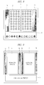
- FIG. 2 is a layout view showing the semiconductor device according to the present embodiment.
- FIG. 2 is an illustration viewing the semiconductor device from a connecting portion side.
- the semiconductor device according to the present embodiment is applied to a non-isolated DC-DC converter as shown in FIG. 1 described above. That is, the semiconductor device of the non-isolated DC-DC converter includes a high-side switch Q 1 , a high-side driver 32 , a low-side switch Q 2 , and a low-side driver 33 .
- the high-side switch Q 1 is configured with a lateral MOSFET whose drain is connected to an input power supply Vin and whose source is connected to an output inductor L.
- the high-side driver 32 is a driver for driving the high-side switch Q 1 and is connected to a gate of the lateral MOSFET of the high-side switch Q 1 .
- the low-side switch Q 2 is configured with a lateral MOSFET whose drain is connected to the output inductor L and whose source is connected to a reference potential GND.
- the low-side driver 33 is a driver for driving the low-side switch Q 2 and is connected to a gate of the lateral MOSFET of the low-side switch Q 2 .
- a high-side switch 2 corresponds to the high-side switch Q 1 (diode D 1 : high-side built-in MOSFET)
- a high-side driver 4 a corresponds to the high-side driver 32
- a low-side switch 3 corresponds to the low-side switch Q 2 (diode D 2 : low-side built-in MOSFET)
- a low-side driver 4 b corresponds to the low-side driver 33
- a controller circuit 5 corresponds to the power supply controller 31 , respectively, and they represent the same components.
- the high-side switch 2 and the low-side switch 3 , the high-side driver 4 a for driving the high-side switch 2 and the low-side driver 4 b for driving the low-side switch 3 , and the controller circuit 5 for controlling the high-side driver 4 a and the low-side driver 4 b are mounted on a semiconductor substrate 1 . More particularly, in the semiconductor device according to the present embodiment, the high-side driver 4 a is arranged in a region closer to a periphery of the semiconductor substrate 1 than the high-side switch 2 , and the low-side driver 4 b is arranged in a region closer to the periphery of the semiconductor substrate 1 than the low-side switch 3 .
- FIG. 3 shows an enlarged layout view of A region of FIG. 2 .
- a gate electrode of an aluminum wire 7 is extended rightward from the high-side driver 4 a in FIG. 3
- a gate electrode of a poly silicon wire 8 is extended so as to branch from the gate electrode of the aluminum wire 7 , so that a source region and a drain region are arranged so as to interpose the gate electrode of the poly silicon wire 8 .
- the MOSFET of the high-side switch 2 is configured with the gate electrode, the source region and the drain region interposing the gate electrode therebetween, and the like.
- the reason of using an aluminum wire for a long wire and a poly silicon wire for a short wire in wires of the gate electrodes is because a resistance of the aluminum wire is lower and the increase of the gate resistance can be suppressed even if the wires are long.
- FIG. 4 is a layout view showing a printed board on which the semiconductor device according to the present embodiment is mounted.
- FIG. 4 shows a state in which the semiconductor substrate 1 is stored in a semiconductor package 18 and they are flip-chip mounted on a printed board 11 . Since the semiconductor substrate 1 is flip-chip mounted, right and left of the semiconductor substrate 1 are inverted with those of FIG. 2 .
- An input capacitor 12 , a boot strap capacitor 13 , and a drive capacitor 14 are arranged so as to surround the semiconductor package 18 . Since the input capacitor 12 is arranged close to the high-side switch 2 and the low-side switch 3 , a path from one terminal of the input capacitor 12 to the other terminal of the input capacitor 12 via the high-side switch 2 and the low-side switch 3 is short, so that the parasitic inductance can be reduced. Further, since the boot strap capacitor 13 is arranged close to the high-side driver 4 a , a path from one terminal of the boot strap capacitor 13 to the other terminal of the boot strap capacitor 13 via the high-side driver 4 a is short, so that the parasitic inductance can be reduced.
- the drive capacitor 14 is arranged close to the low-side driver 4 b , a path from one terminal of the drive capacitor 14 to the other terminal of the drive capacitor 14 via the low-side driver 4 b is short, so that the parasitic inductance can be reduced. As a result, this leads to the improvement of the power conversion efficiency.
- the input capacitor 12 corresponds to the input capacitor Cin
- the boot strap capacitor 13 corresponds to the boot strap capacitor Cboot
- the drive capacitor 14 corresponds to the drive capacitor Cdrive, respectively.
- FIG. 5 is a layout view showing a state where wires of the path from a positive terminal of the input power supply Vin to a negative terminal of the input power supply Vin via the high-side switch Q 1 ( 2 ) and the low-side switch Q 2 ( 3 ) are added to the printed board 11 of FIG. 4 .
- a power supply wire 15 connected to the positive terminal of the input power supply Vin and a reference potential wire (GND wire) 16 connected to the negative terminal of the input power supply Vin are arranged close to each other.
- This aims to cancel the magnetic flux caused in switching of the high-side switch 2 by arranging the power supply wire 15 and the reference potential wire 16 close to each other, thereby reducing the effective parasitic inductance. Meanwhile, it is not required to consider a parasitic inductance in an output wire 17 connected to the output inductor L. However, since reduction of its conversion efficiency due to the wire resistance is concerned, it is necessary to ensure a sufficiently large wire width.
- FIG. 6 is a layout view describing a connecting portion between the semiconductor package 18 or the printed board 11 and the semiconductor substrate 1 on which the high-side switch 2 , the low-side switch 3 , and the controller circuit 5 are formed.
- FIG. 6 shows an example of using bumps 6 for the connection of the semiconductor substrate 1 on which the high-side switch 2 , the low-side switch 3 , and the controller circuit 5 are formed.
- the semiconductor substrate 1 is connected to the printed board 11 via the bumps 6 .
- the semiconductor package 18 is connected to the printed board 11 via the bumps 6 .
- the bumps 6 are used for the connecting portion in both of the semiconductor device in the state of the semiconductor substrate 1 and the semiconductor device in which the semiconductor substrate 1 is stored in the semiconductor package 18 .
- the wire bonding used for the connection between the semiconductor substrate 1 and the semiconductor package 18 has following problems. That is, an upper limit of the number of pins is low because bonding pads have to be provided in the periphery of the semiconductor substrate 1 , and the wire resistance is high because the wires have to be led to the pads arranged in the periphery of the semiconductor substrate 1 . Compared to this, since the bumps 6 can be the connecting portion in the whole semiconductor substrate 1 , many pins can be provided. Also, since the connection is made from the center region of the semiconductor substrate 1 to the semiconductor package 18 or the printed board 11 via the bumps 6 , the increase of the wire resistance caused by leading the wires of the semiconductor substrate 1 can be suppressed.
- FIG. 7 is a layout view arranged with focusing on the potential of the bumps of the high-side switch 2 and the low-side switch 3 .
- bumps 21 corresponding to the drain potential of the high-side switch 2 are connected to the positive terminal of the input power supply Vin
- bumps 23 corresponding to the source potential of the high-side switch 2 and the drain potential of the low-side switch 3 are connected to one terminal of the output inductor L
- bumps 22 corresponding to the source potential of the low-side switch 3 are connected to the negative terminal of the input power supply Vin.
- the bumps 21 corresponding to the drain potential and the bumps 23 corresponding to the source potential are alternately arranged in a vertical direction in the high-side switch 2
- the bumps 22 corresponding to the source potential and the bumps 23 corresponding to the drain potential are alternately arranged in a vertical direction in the low-side switch 3
- the bumps 23 are arranged at the same positions in the high-side switch 2 and the low-side switch 3 when viewed in a vertical direction.
- FIG. 8 is a layout view arranged with focusing on the source electrodes and the drain electrodes of the bumps of the high-side switch 2 and the low-side switch 3 .
- a symbol “S” indicates the source and a symbol “D” indicates the drain, respectively.
- the bump of the source S and the bump of the drain D are alternately arranged in a lateral direction, and further, the bump of the source S and the bump of the drain D are alternately arranged also in a vertical direction.
- the bump of the source S and the bump of the drain D are alternately arranged in lateral and vertical directions.
- the high-side driver 4 a is arranged in a region closer to the periphery of the semiconductor substrate 1 than the high-side switch 2
- the low-side driver 4 b is arranged in a region closer to the periphery of the semiconductor substrate 1 than the low-side switch 3 , and therefore, the paths among the input capacitor 12 , the boot strap capacitor 13 , and the drive capacitor 14 are shortened. As a result, the parasitic inductance is reduced, and the conversion efficiency can be improved.
- FIG. 9 is a layout view showing a semiconductor device according to a second embodiment of the present invention.
- a different point of the semiconductor device according to the present embodiment from that of the first embodiment is that not only the high-side driver 4 a and the low-side driver 4 b arranged in the regions closer to the periphery of the semiconductor substrate 1 but also a high-side driver 4 c and a low-side driver 4 d arranged in a region closer to the center of the semiconductor substrate 1 are provided as the drivers for the high-side switch 2 and the low-side switch 3 .
- a voltage of the input power supply Vin is 12 V and its output voltage is approximately 1 V to be an operation voltage of the CPU 34 , and therefore, the ON ratio of the high-side switch Q 1 is as low as approximately one twelfth. Accordingly, most of the loss component of the low-side switch Q 2 is the conduction loss, and therefore, it is effective to reduce the ON resistance of the low-side switch Q 2 for the improvement of the conversion efficiency.
- the high-side drivers 4 a and 4 c are arranged in the regions closer to the periphery of the semiconductor substrate 1 and the center of the semiconductor substrate 1 than the high-side switch 2
- the low-side drivers 4 b and 4 d are arranged in the regions closer to the periphery of the semiconductor substrate 1 and the center of the semiconductor substrate 1 than the low-side switch 3 , and therefore, the parasitic inductance can be further reduced and the conversion efficiency can be further improved compared to the first embodiment.
- the further improvement of the conversion efficiency is possible by devising the arrangement of the power supply wire and the reference potential wire and the arrangement of the output wire, and using the bumps for the connecting portion and devising the arrangement of the bumps.
- a semiconductor device used as the switches is a lateral MOSFET.
- the source region and the drain region are formed on a surface of the semiconductor substrate, and the source electrode and the drain electrode are also formed on the surface of the semiconductor substrate (one example of the lateral MOSFET is disclosed in Patent Document 1).
- the lateral MOSFET can have a large current capacity per unit area of the semiconductor substrate when breakdown voltage is low, but it is required to lengthen a distance between the source and the drain in the lateral direction when breakdown voltage is high, and therefore, the current capacity becomes small.
- a region for maintaining the voltage between the source and the drain is arranged in the vertical direction of the semiconductor substrate, and it is not required to lengthen the distance in the lateral direction of the semiconductor substrate even when breakdown voltage becomes high, and therefore, the current capacity per unit area of the semiconductor substrate can be increased compared to the lateral MOSFET in a device with high breakdown voltage over 30 V, so that the ON resistance can be reduced (the vertical MOSFET is disclosed in, for example, Japanese Patent Application Laid-Open Publication No. 2005-57050).
- FIG. 10 is a layout view showing a semiconductor device according to the third embodiment of the present invention.
- FIG. 10 shows the semiconductor substrate 1 on which the high-side switch 2 , the high-side driver 4 a for driving the high-side switch 2 , the low-side driver 4 b for driving the low-side switch 3 , and the controller circuit 5 for controlling the high-side driver 4 a and the low-side driver 4 b are mounted in the case where the low-side switch 3 is mounted on the different semiconductor substrate from the semiconductor substrate 1 .
- the high-side driver 4 a and the low-side driver 4 b are arranged in the regions closer to the periphery of the semiconductor substrate 1 than the high-side switch 2 .
- the path among the input capacitor 12 , the boot strap capacitor 13 , and the drive capacitor 14 , which are arranged so as to surround the semiconductor device becomes short, so that the parasitic inductance can be reduced.
- the semiconductor substrate 1 on which the high-side switch 2 , the high-side driver 4 a , the low-side driver 4 b , and the controller circuit 5 are mounted and the semiconductor substrate on which the low-side switch 3 is mounted are stored in the same semiconductor package.
- the further improvement of the conversion efficiency is possible by devising the arrangement of the power supply wire and the reference potential wire and the arrangement of the output wire, and using the bumps for the connecting portion and devising the arrangement of the bumps.
- the semiconductor device according to the present invention can be used for a semiconductor device used for a power converter such as a power supply. More particularly, the semiconductor device is effectively applied to a non-isolated DC-DC converter.
Landscapes
- Engineering & Computer Science (AREA)
- Power Engineering (AREA)
- Dc-Dc Converters (AREA)
- Semiconductor Integrated Circuits (AREA)
Abstract
Description
Claims (6)
Applications Claiming Priority (3)
| Application Number | Priority Date | Filing Date | Title |
|---|---|---|---|
| JP2008172165A JP5297104B2 (en) | 2008-07-01 | 2008-07-01 | Semiconductor device |
| JP2008-172165 | 2008-07-01 | ||
| JPJP2008-172165 | 2008-07-01 |
Publications (2)
| Publication Number | Publication Date |
|---|---|
| US20100001790A1 US20100001790A1 (en) | 2010-01-07 |
| US8203380B2 true US8203380B2 (en) | 2012-06-19 |
Family
ID=41463899
Family Applications (1)
| Application Number | Title | Priority Date | Filing Date |
|---|---|---|---|
| US12/483,668 Expired - Fee Related US8203380B2 (en) | 2008-07-01 | 2009-06-12 | Semiconductor device |
Country Status (3)
| Country | Link |
|---|---|
| US (1) | US8203380B2 (en) |
| JP (1) | JP5297104B2 (en) |
| CN (2) | CN101621061B (en) |
Cited By (6)
| Publication number | Priority date | Publication date | Assignee | Title |
|---|---|---|---|---|
| US20150001618A1 (en) * | 2013-06-28 | 2015-01-01 | Magnachip Semiconductor, Ltd. | Semiconductor package |
| US20150035580A1 (en) * | 2013-07-31 | 2015-02-05 | Stmicroelectronics S.R.I. | Power electronic device with improved efficiency and electromagnetic radiation characteristics |
| US9236321B2 (en) | 2012-02-15 | 2016-01-12 | Renesas Electronics Corporation | Semiconductor device and manufacturing method thereof |
| US20170155377A1 (en) * | 2015-12-01 | 2017-06-01 | Delta Electronics, Inc. | Driving circuit for power switch |
| US20230111993A1 (en) * | 2014-09-16 | 2023-04-13 | Navitas Semiconductor Limited | Half-bridge circuit using separately packaged gan power devices |
| US20250337323A1 (en) * | 2024-04-26 | 2025-10-30 | Analog Devices, Inc. | Semiconductor dice for inductor-based switching power converters and associated integrated circuits and systems |
Families Citing this family (19)
| Publication number | Priority date | Publication date | Assignee | Title |
|---|---|---|---|---|
| JP4405529B2 (en) * | 2007-05-15 | 2010-01-27 | 株式会社東芝 | Semiconductor device |
| US8680895B2 (en) * | 2010-10-08 | 2014-03-25 | Texas Instruments Incorporated | Controlling power chain with same controller in either of two different applications |
| JP2013017360A (en) | 2011-07-06 | 2013-01-24 | Toshiba Corp | Semiconductor device, dc-dc converter, and image receiver |
| KR101933462B1 (en) * | 2011-10-19 | 2019-01-02 | 삼성전자주식회사 | Wireless power receiver for controlling magnitude of wireless power |
| JP5805513B2 (en) | 2011-12-14 | 2015-11-04 | 三菱電機株式会社 | Power semiconductor device |
| JP6077864B2 (en) * | 2013-01-21 | 2017-02-08 | 株式会社小糸製作所 | DC-DC converter, vehicle lamp |
| CN104969342B (en) * | 2013-03-01 | 2019-03-01 | 富士电机株式会社 | semiconductor device |
| JP6156643B2 (en) * | 2013-09-25 | 2017-07-05 | 東芝ライテック株式会社 | Power supply device and lighting device |
| JP6295065B2 (en) | 2013-11-20 | 2018-03-14 | ルネサスエレクトロニクス株式会社 | Semiconductor device |
| US9825553B2 (en) * | 2014-04-17 | 2017-11-21 | Linear Technology Corporation | Voltage regulation in resonant power wireless receiver |
| US9419509B2 (en) * | 2014-08-11 | 2016-08-16 | Texas Instruments Incorporated | Shared bootstrap capacitor for multiple phase buck converter circuit and methods |
| JP2016207783A (en) * | 2015-04-20 | 2016-12-08 | シャープ株式会社 | Power module |
| US10069439B2 (en) * | 2015-12-22 | 2018-09-04 | Renesas Electronics Corporation | Power conversion system, power module, and semiconductor device with diode coupling |
| ITUA20161531A1 (en) * | 2016-03-10 | 2017-09-10 | St Microelectronics Srl | DIODE WITH REDUCED RECOVERY TIME FOR APPLICATIONS SUBJECT TO THE CURRENT RECIRCULATION PHENOMENON AND / OR TO RAPID VOLTAGE VARIATIONS |
| IT201600088211A1 (en) | 2016-08-30 | 2018-03-02 | St Microelectronics Srl | JUNCTION ELECTRONIC DEVICE WITH REDUCED RECOVERY TIME FOR APPLICATIONS SUBJECT TO THE PHENOMENON OF THE CURRENT RECIRCULATION AND RELATIVE MANUFACTURING METHOD |
| JP7011831B2 (en) * | 2016-09-23 | 2022-01-27 | 国立大学法人東北大学 | Switching circuit equipment and step-down DC-DC converter |
| JP6388181B2 (en) * | 2017-06-08 | 2018-09-12 | 東芝ライテック株式会社 | Semiconductor package and power supply device |
| JP7231382B2 (en) * | 2018-11-06 | 2023-03-01 | ローム株式会社 | semiconductor equipment |
| US11616006B2 (en) * | 2019-02-27 | 2023-03-28 | Semiconductor Components Industries, Llc | Semiconductor package with heatsink |
Citations (5)
| Publication number | Priority date | Publication date | Assignee | Title |
|---|---|---|---|---|
| US6114903A (en) * | 1998-01-14 | 2000-09-05 | Lsi Logic Corporation | Layout architecture for core I/O buffer |
| US6460168B1 (en) * | 1998-04-23 | 2002-10-01 | Matsushita Electric Industrial Co., Ltd. | Method of designing power supply circuit and semiconductor chip |
| JP2005057050A (en) | 2003-08-04 | 2005-03-03 | Renesas Technology Corp | Semiconductor device and manufacturing method thereof |
| JP2005203766A (en) | 2003-12-18 | 2005-07-28 | Toshiba Corp | Semiconductor integrated circuit device |
| US20070170897A1 (en) * | 2006-01-26 | 2007-07-26 | Advanced Analogic Technologies, Inc. | High-Frequency Power MESFET Buck Switching Power Supply |
Family Cites Families (6)
| Publication number | Priority date | Publication date | Assignee | Title |
|---|---|---|---|---|
| JP2001085627A (en) * | 1999-09-16 | 2001-03-30 | Sharp Corp | Switching power supply |
| JP4115882B2 (en) * | 2003-05-14 | 2008-07-09 | 株式会社ルネサステクノロジ | Semiconductor device |
| US7138698B2 (en) * | 2003-12-18 | 2006-11-21 | Kabushiki Kaisha Toshiba | Semiconductor device including power MOS field-effect transistor and driver circuit driving thereof |
| JP2006245405A (en) * | 2005-03-04 | 2006-09-14 | Matsushita Electric Ind Co Ltd | Semiconductor device and motor drive device using the same |
| JP2007103721A (en) * | 2005-10-05 | 2007-04-19 | Toshiba Corp | DC-DC converter |
| JP2008140824A (en) * | 2006-11-30 | 2008-06-19 | Toshiba Corp | Semiconductor device |
-
2008
- 2008-07-01 JP JP2008172165A patent/JP5297104B2/en active Active
-
2009
- 2009-06-12 US US12/483,668 patent/US8203380B2/en not_active Expired - Fee Related
- 2009-07-01 CN CN2009101509802A patent/CN101621061B/en active Active
- 2009-07-01 CN CN2011104198179A patent/CN102522405A/en active Pending
Patent Citations (5)
| Publication number | Priority date | Publication date | Assignee | Title |
|---|---|---|---|---|
| US6114903A (en) * | 1998-01-14 | 2000-09-05 | Lsi Logic Corporation | Layout architecture for core I/O buffer |
| US6460168B1 (en) * | 1998-04-23 | 2002-10-01 | Matsushita Electric Industrial Co., Ltd. | Method of designing power supply circuit and semiconductor chip |
| JP2005057050A (en) | 2003-08-04 | 2005-03-03 | Renesas Technology Corp | Semiconductor device and manufacturing method thereof |
| JP2005203766A (en) | 2003-12-18 | 2005-07-28 | Toshiba Corp | Semiconductor integrated circuit device |
| US20070170897A1 (en) * | 2006-01-26 | 2007-07-26 | Advanced Analogic Technologies, Inc. | High-Frequency Power MESFET Buck Switching Power Supply |
Cited By (16)
| Publication number | Priority date | Publication date | Assignee | Title |
|---|---|---|---|---|
| US9236321B2 (en) | 2012-02-15 | 2016-01-12 | Renesas Electronics Corporation | Semiconductor device and manufacturing method thereof |
| US9991192B2 (en) | 2013-06-28 | 2018-06-05 | Magnachip Semiconductor, Ltd. | Semiconductor package |
| US9601453B2 (en) * | 2013-06-28 | 2017-03-21 | Magnachip Semiconductor, Ltd. | Semiconductor package |
| US20150001618A1 (en) * | 2013-06-28 | 2015-01-01 | Magnachip Semiconductor, Ltd. | Semiconductor package |
| US20150035580A1 (en) * | 2013-07-31 | 2015-02-05 | Stmicroelectronics S.R.I. | Power electronic device with improved efficiency and electromagnetic radiation characteristics |
| US9602096B2 (en) * | 2013-07-31 | 2017-03-21 | Stmicroelectronics S.R.L. | Power electronic device with improved efficiency and electromagnetic radiation characteristics |
| US11770010B2 (en) * | 2014-09-16 | 2023-09-26 | Navitas Semiconductor Limited | Half-bridge circuit using separately packaged GaN power devices |
| US20230111993A1 (en) * | 2014-09-16 | 2023-04-13 | Navitas Semiconductor Limited | Half-bridge circuit using separately packaged gan power devices |
| US11757290B2 (en) | 2014-09-16 | 2023-09-12 | Navitas Semiconductor Limited | Half-bridge circuit using flip-chip GaN power devices |
| US11862996B2 (en) | 2014-09-16 | 2024-01-02 | Navitas Semiconductor Limited | Pulsed level shift and inverter circuits for GaN devices |
| US11888332B2 (en) | 2014-09-16 | 2024-01-30 | Navitas Semiconductor Limited | Half-bridge circuit using monolithic flip-chip GaN power devices |
| US10483949B2 (en) * | 2015-12-01 | 2019-11-19 | Delta Electronics, Inc. | Driving circuit for power switch |
| US20190379362A1 (en) * | 2015-12-01 | 2019-12-12 | Delta Electronics, Inc. | Driving circuit for power switch |
| US10734976B2 (en) * | 2015-12-01 | 2020-08-04 | Delta Electronics, Inc. | Driving circuit for power switch |
| US20170155377A1 (en) * | 2015-12-01 | 2017-06-01 | Delta Electronics, Inc. | Driving circuit for power switch |
| US20250337323A1 (en) * | 2024-04-26 | 2025-10-30 | Analog Devices, Inc. | Semiconductor dice for inductor-based switching power converters and associated integrated circuits and systems |
Also Published As
| Publication number | Publication date |
|---|---|
| CN101621061B (en) | 2012-02-15 |
| JP2010016035A (en) | 2010-01-21 |
| US20100001790A1 (en) | 2010-01-07 |
| CN101621061A (en) | 2010-01-06 |
| CN102522405A (en) | 2012-06-27 |
| JP5297104B2 (en) | 2013-09-25 |
Similar Documents
| Publication | Publication Date | Title |
|---|---|---|
| US8203380B2 (en) | Semiconductor device | |
| US8638577B2 (en) | Semiconductor device for DC-DC converter including high side and low side semiconductor switches | |
| US10896896B2 (en) | Semiconductor device comprising PN junction diode and schottky barrier diode | |
| US8008699B2 (en) | Semiconductor device with circuit for reduced parasitic inductance | |
| US8018255B2 (en) | DC-DC converter, driver IC, and system in package | |
| US8476885B2 (en) | Monolithic group III-V power converter | |
| US20110181255A1 (en) | Semiconductor device and power supply unit using the same | |
| US8643102B2 (en) | Control device of semiconductor device | |
| KR20110015043A (en) | Semiconductor device and power supply system | |
| US11990455B2 (en) | Semiconductor device | |
| JP5191689B2 (en) | Semiconductor device | |
| JP5214675B2 (en) | Semiconductor device | |
| US20130257524A1 (en) | Monolithic Power Converter Package | |
| CN111341749B (en) | Semiconductor module |
Legal Events
| Date | Code | Title | Description |
|---|---|---|---|
| AS | Assignment |
Owner name: RENESAS TECHNOLOGY CORP., JAPAN Free format text: ASSIGNMENT OF ASSIGNORS INTEREST;ASSIGNORS:HASHIMOTO, TAKAYUKI;HIRAO, TAKASHI;AKIYAMA, NOBORU;REEL/FRAME:023521/0400;SIGNING DATES FROM 20090807 TO 20090820 Owner name: RENESAS TECHNOLOGY CORP., JAPAN Free format text: ASSIGNMENT OF ASSIGNORS INTEREST;ASSIGNORS:HASHIMOTO, TAKAYUKI;HIRAO, TAKASHI;AKIYAMA, NOBORU;SIGNING DATES FROM 20090807 TO 20090820;REEL/FRAME:023521/0400 |
|
| AS | Assignment |
Owner name: RENESAS ELECTRONICS CORPORATION, JAPAN Free format text: CHANGE OF NAME;ASSIGNOR:NEC ELECTRONICS CORPORATION;REEL/FRAME:024988/0161 Effective date: 20100401 Owner name: NEC ELECTRONICS CORPORATION, JAPAN Free format text: MERGER;ASSIGNOR:RENESAS TECHNOLOGY CORP.;REEL/FRAME:024987/0833 Effective date: 20100401 |
|
| REMI | Maintenance fee reminder mailed | ||
| LAPS | Lapse for failure to pay maintenance fees | ||
| STCH | Information on status: patent discontinuation |
Free format text: PATENT EXPIRED DUE TO NONPAYMENT OF MAINTENANCE FEES UNDER 37 CFR 1.362 |
|
| STCH | Information on status: patent discontinuation |
Free format text: PATENT EXPIRED DUE TO NONPAYMENT OF MAINTENANCE FEES UNDER 37 CFR 1.362 |
|
| FP | Lapsed due to failure to pay maintenance fee |
Effective date: 20160619 |