US8159640B2 - Liquid crystal display device - Google Patents
Liquid crystal display device Download PDFInfo
- Publication number
- US8159640B2 US8159640B2 US12/441,445 US44144507A US8159640B2 US 8159640 B2 US8159640 B2 US 8159640B2 US 44144507 A US44144507 A US 44144507A US 8159640 B2 US8159640 B2 US 8159640B2
- Authority
- US
- United States
- Prior art keywords
- liquid crystal
- alignment
- pixel electrode
- corner portion
- alignment control
- Prior art date
- Legal status (The legal status is an assumption and is not a legal conclusion. Google has not performed a legal analysis and makes no representation as to the accuracy of the status listed.)
- Active, expires
Links
- 239000004973 liquid crystal related substance Substances 0.000 title claims abstract description 83
- 230000007246 mechanism Effects 0.000 claims abstract description 33
- 230000005684 electric field Effects 0.000 abstract description 8
- 239000000758 substrate Substances 0.000 description 42
- 239000010410 layer Substances 0.000 description 40
- 239000011521 glass Substances 0.000 description 24
- 239000010408 film Substances 0.000 description 22
- 239000000463 material Substances 0.000 description 15
- 239000004020 conductor Substances 0.000 description 6
- 239000011229 interlayer Substances 0.000 description 6
- 238000000206 photolithography Methods 0.000 description 6
- 238000000034 method Methods 0.000 description 5
- 230000002349 favourable effect Effects 0.000 description 4
- 239000011159 matrix material Substances 0.000 description 4
- 229920001721 polyimide Polymers 0.000 description 4
- 239000004065 semiconductor Substances 0.000 description 4
- 238000004544 sputter deposition Methods 0.000 description 3
- 239000004925 Acrylic resin Substances 0.000 description 2
- 229920000178 Acrylic resin Polymers 0.000 description 2
- 239000004642 Polyimide Substances 0.000 description 2
- 229910052581 Si3N4 Inorganic materials 0.000 description 2
- XAGFODPZIPBFFR-UHFFFAOYSA-N aluminium Chemical compound [Al] XAGFODPZIPBFFR-UHFFFAOYSA-N 0.000 description 2
- 229910052782 aluminium Inorganic materials 0.000 description 2
- 229910021417 amorphous silicon Inorganic materials 0.000 description 2
- 230000005540 biological transmission Effects 0.000 description 2
- 239000003086 colorant Substances 0.000 description 2
- 238000010438 heat treatment Methods 0.000 description 2
- 238000007641 inkjet printing Methods 0.000 description 2
- 239000007788 liquid Substances 0.000 description 2
- 238000004519 manufacturing process Methods 0.000 description 2
- 238000000059 patterning Methods 0.000 description 2
- 238000005268 plasma chemical vapour deposition Methods 0.000 description 2
- 239000009719 polyimide resin Substances 0.000 description 2
- 238000007639 printing Methods 0.000 description 2
- 239000011342 resin composition Substances 0.000 description 2
- 239000003566 sealing material Substances 0.000 description 2
- HQVNEWCFYHHQES-UHFFFAOYSA-N silicon nitride Chemical compound N12[Si]34N5[Si]62N3[Si]51N64 HQVNEWCFYHHQES-UHFFFAOYSA-N 0.000 description 2
- VYZAMTAEIAYCRO-UHFFFAOYSA-N Chromium Chemical compound [Cr] VYZAMTAEIAYCRO-UHFFFAOYSA-N 0.000 description 1
- RTAQQCXQSZGOHL-UHFFFAOYSA-N Titanium Chemical compound [Ti] RTAQQCXQSZGOHL-UHFFFAOYSA-N 0.000 description 1
- 229910052804 chromium Inorganic materials 0.000 description 1
- 239000011651 chromium Substances 0.000 description 1
- 238000004040 coloring Methods 0.000 description 1
- 238000011156 evaluation Methods 0.000 description 1
- AMGQUBHHOARCQH-UHFFFAOYSA-N indium;oxotin Chemical compound [In].[Sn]=O AMGQUBHHOARCQH-UHFFFAOYSA-N 0.000 description 1
- 239000000976 ink Substances 0.000 description 1
- 230000001788 irregular Effects 0.000 description 1
- 238000012986 modification Methods 0.000 description 1
- 230000004048 modification Effects 0.000 description 1
- 230000003071 parasitic effect Effects 0.000 description 1
- 229920002120 photoresistant polymer Polymers 0.000 description 1
- 239000000049 pigment Substances 0.000 description 1
- 230000010287 polarization Effects 0.000 description 1
- 230000001902 propagating effect Effects 0.000 description 1
- 239000011347 resin Substances 0.000 description 1
- 229920005989 resin Polymers 0.000 description 1
- 238000007789 sealing Methods 0.000 description 1
- 239000002356 single layer Substances 0.000 description 1
- 239000010409 thin film Substances 0.000 description 1
- 239000010936 titanium Substances 0.000 description 1
- 229910052719 titanium Inorganic materials 0.000 description 1
- 238000002834 transmittance Methods 0.000 description 1
- WFKWXMTUELFFGS-UHFFFAOYSA-N tungsten Chemical compound [W] WFKWXMTUELFFGS-UHFFFAOYSA-N 0.000 description 1
- 229910052721 tungsten Inorganic materials 0.000 description 1
- 239000010937 tungsten Substances 0.000 description 1
Images


Classifications
-
- G—PHYSICS
- G02—OPTICS
- G02F—OPTICAL DEVICES OR ARRANGEMENTS FOR THE CONTROL OF LIGHT BY MODIFICATION OF THE OPTICAL PROPERTIES OF THE MEDIA OF THE ELEMENTS INVOLVED THEREIN; NON-LINEAR OPTICS; FREQUENCY-CHANGING OF LIGHT; OPTICAL LOGIC ELEMENTS; OPTICAL ANALOGUE/DIGITAL CONVERTERS
- G02F1/00—Devices or arrangements for the control of the intensity, colour, phase, polarisation or direction of light arriving from an independent light source, e.g. switching, gating or modulating; Non-linear optics
- G02F1/01—Devices or arrangements for the control of the intensity, colour, phase, polarisation or direction of light arriving from an independent light source, e.g. switching, gating or modulating; Non-linear optics for the control of the intensity, phase, polarisation or colour
- G02F1/13—Devices or arrangements for the control of the intensity, colour, phase, polarisation or direction of light arriving from an independent light source, e.g. switching, gating or modulating; Non-linear optics for the control of the intensity, phase, polarisation or colour based on liquid crystals, e.g. single liquid crystal display cells
- G02F1/137—Devices or arrangements for the control of the intensity, colour, phase, polarisation or direction of light arriving from an independent light source, e.g. switching, gating or modulating; Non-linear optics for the control of the intensity, phase, polarisation or colour based on liquid crystals, e.g. single liquid crystal display cells characterised by the electro-optical or magneto-optical effect, e.g. field-induced phase transition, orientation effect, guest-host interaction or dynamic scattering
- G02F1/139—Devices or arrangements for the control of the intensity, colour, phase, polarisation or direction of light arriving from an independent light source, e.g. switching, gating or modulating; Non-linear optics for the control of the intensity, phase, polarisation or colour based on liquid crystals, e.g. single liquid crystal display cells characterised by the electro-optical or magneto-optical effect, e.g. field-induced phase transition, orientation effect, guest-host interaction or dynamic scattering based on orientation effects in which the liquid crystal remains transparent
- G02F1/1393—Devices or arrangements for the control of the intensity, colour, phase, polarisation or direction of light arriving from an independent light source, e.g. switching, gating or modulating; Non-linear optics for the control of the intensity, phase, polarisation or colour based on liquid crystals, e.g. single liquid crystal display cells characterised by the electro-optical or magneto-optical effect, e.g. field-induced phase transition, orientation effect, guest-host interaction or dynamic scattering based on orientation effects in which the liquid crystal remains transparent the birefringence of the liquid crystal being electrically controlled, e.g. ECB-, DAP-, HAN-, PI-LC cells
-
- G—PHYSICS
- G02—OPTICS
- G02F—OPTICAL DEVICES OR ARRANGEMENTS FOR THE CONTROL OF LIGHT BY MODIFICATION OF THE OPTICAL PROPERTIES OF THE MEDIA OF THE ELEMENTS INVOLVED THEREIN; NON-LINEAR OPTICS; FREQUENCY-CHANGING OF LIGHT; OPTICAL LOGIC ELEMENTS; OPTICAL ANALOGUE/DIGITAL CONVERTERS
- G02F1/00—Devices or arrangements for the control of the intensity, colour, phase, polarisation or direction of light arriving from an independent light source, e.g. switching, gating or modulating; Non-linear optics
- G02F1/01—Devices or arrangements for the control of the intensity, colour, phase, polarisation or direction of light arriving from an independent light source, e.g. switching, gating or modulating; Non-linear optics for the control of the intensity, phase, polarisation or colour
- G02F1/13—Devices or arrangements for the control of the intensity, colour, phase, polarisation or direction of light arriving from an independent light source, e.g. switching, gating or modulating; Non-linear optics for the control of the intensity, phase, polarisation or colour based on liquid crystals, e.g. single liquid crystal display cells
- G02F1/133—Constructional arrangements; Operation of liquid crystal cells; Circuit arrangements
- G02F1/1333—Constructional arrangements; Manufacturing methods
- G02F1/1337—Surface-induced orientation of the liquid crystal molecules, e.g. by alignment layers
- G02F1/133707—Structures for producing distorted electric fields, e.g. bumps, protrusions, recesses, slits in pixel electrodes
-
- G—PHYSICS
- G02—OPTICS
- G02F—OPTICAL DEVICES OR ARRANGEMENTS FOR THE CONTROL OF LIGHT BY MODIFICATION OF THE OPTICAL PROPERTIES OF THE MEDIA OF THE ELEMENTS INVOLVED THEREIN; NON-LINEAR OPTICS; FREQUENCY-CHANGING OF LIGHT; OPTICAL LOGIC ELEMENTS; OPTICAL ANALOGUE/DIGITAL CONVERTERS
- G02F1/00—Devices or arrangements for the control of the intensity, colour, phase, polarisation or direction of light arriving from an independent light source, e.g. switching, gating or modulating; Non-linear optics
- G02F1/01—Devices or arrangements for the control of the intensity, colour, phase, polarisation or direction of light arriving from an independent light source, e.g. switching, gating or modulating; Non-linear optics for the control of the intensity, phase, polarisation or colour
- G02F1/13—Devices or arrangements for the control of the intensity, colour, phase, polarisation or direction of light arriving from an independent light source, e.g. switching, gating or modulating; Non-linear optics for the control of the intensity, phase, polarisation or colour based on liquid crystals, e.g. single liquid crystal display cells
- G02F1/133—Constructional arrangements; Operation of liquid crystal cells; Circuit arrangements
- G02F1/1333—Constructional arrangements; Manufacturing methods
- G02F1/1337—Surface-induced orientation of the liquid crystal molecules, e.g. by alignment layers
- G02F1/133753—Surface-induced orientation of the liquid crystal molecules, e.g. by alignment layers with different alignment orientations or pretilt angles on a same surface, e.g. for grey scale or improved viewing angle
-
- G—PHYSICS
- G02—OPTICS
- G02F—OPTICAL DEVICES OR ARRANGEMENTS FOR THE CONTROL OF LIGHT BY MODIFICATION OF THE OPTICAL PROPERTIES OF THE MEDIA OF THE ELEMENTS INVOLVED THEREIN; NON-LINEAR OPTICS; FREQUENCY-CHANGING OF LIGHT; OPTICAL LOGIC ELEMENTS; OPTICAL ANALOGUE/DIGITAL CONVERTERS
- G02F1/00—Devices or arrangements for the control of the intensity, colour, phase, polarisation or direction of light arriving from an independent light source, e.g. switching, gating or modulating; Non-linear optics
- G02F1/01—Devices or arrangements for the control of the intensity, colour, phase, polarisation or direction of light arriving from an independent light source, e.g. switching, gating or modulating; Non-linear optics for the control of the intensity, phase, polarisation or colour
- G02F1/13—Devices or arrangements for the control of the intensity, colour, phase, polarisation or direction of light arriving from an independent light source, e.g. switching, gating or modulating; Non-linear optics for the control of the intensity, phase, polarisation or colour based on liquid crystals, e.g. single liquid crystal display cells
- G02F1/133—Constructional arrangements; Operation of liquid crystal cells; Circuit arrangements
- G02F1/1333—Constructional arrangements; Manufacturing methods
- G02F1/1343—Electrodes
- G02F1/134309—Electrodes characterised by their geometrical arrangement
- G02F1/134336—Matrix
-
- G—PHYSICS
- G02—OPTICS
- G02F—OPTICAL DEVICES OR ARRANGEMENTS FOR THE CONTROL OF LIGHT BY MODIFICATION OF THE OPTICAL PROPERTIES OF THE MEDIA OF THE ELEMENTS INVOLVED THEREIN; NON-LINEAR OPTICS; FREQUENCY-CHANGING OF LIGHT; OPTICAL LOGIC ELEMENTS; OPTICAL ANALOGUE/DIGITAL CONVERTERS
- G02F2201/00—Constructional arrangements not provided for in groups G02F1/00 - G02F7/00
- G02F2201/12—Constructional arrangements not provided for in groups G02F1/00 - G02F7/00 electrode
- G02F2201/121—Constructional arrangements not provided for in groups G02F1/00 - G02F7/00 electrode common or background
-
- G—PHYSICS
- G02—OPTICS
- G02F—OPTICAL DEVICES OR ARRANGEMENTS FOR THE CONTROL OF LIGHT BY MODIFICATION OF THE OPTICAL PROPERTIES OF THE MEDIA OF THE ELEMENTS INVOLVED THEREIN; NON-LINEAR OPTICS; FREQUENCY-CHANGING OF LIGHT; OPTICAL LOGIC ELEMENTS; OPTICAL ANALOGUE/DIGITAL CONVERTERS
- G02F2201/00—Constructional arrangements not provided for in groups G02F1/00 - G02F7/00
- G02F2201/12—Constructional arrangements not provided for in groups G02F1/00 - G02F7/00 electrode
- G02F2201/123—Constructional arrangements not provided for in groups G02F1/00 - G02F7/00 electrode pixel
Definitions
- the present invention relates to a liquid crystal display device using a vertical alignment mode which has excellent image display quality.
- a liquid crystal display device is in widespread use as a display of a household electrical appliance such as a personal computer and a television set.
- a liquid crystal panel is used which includes two glass substrates between which a liquid crystal is filled in a space surrounded by a sealing member.
- a liquid crystal display device using a vertical alignment mode is commercially practical, in which a liquid crystal layer possessing negative dielectric anisotropy is interposed between an opposed glass substrate pair such that liquid crystal molecules are aligned vertically, and when a voltage is applied to the liquid crystal layer, the liquid crystal molecules are controlled to be aligned in a plurality of inclined directions relative to the glass substrates.
- the liquid crystal molecules are aligned vertically relative to the opposed glass substrate pair in a state where no voltage is applied thereto which defines a non-driven state, so that light which passes through the liquid crystal layer has its polarization plane little changed.
- black display can be achieved almost perfectly in the state where no voltage is applied thereto, and thereby a high-contrast image is obtained.
- a reference numeral 58 indicates equipotential lines at the time when a voltage is applied
- a reference numeral 59 indicates an oblique electric field (a fringe field).
- a pair of gate bus lines 11 and a pair of source bus lines 12 which are perpendicular to each other are arranged in a grid pattern, and a pixel electrode 51 is provided in a pixel region surrounded by the gate bus lines 11 and the source bus lines 12 .
- openings 57 of slits are formed to extend in an oblique direction.
- the openings 57 are provided and arranged to generate an oblique electric field (a fringe field) at the time when a voltage is applied and to control liquid crystal molecule alignment in order to improve viewing angle characteristics as mentioned above.
- the openings 57 which are oblique at a given angle are arranged to be vertically symmetrical in each pixel electrode 51 as shown in FIG. 8 .
- linear protrusions 55 a to 55 c are provided under the common electrode 52 (not shown in FIG. 8 ).
- the linear protrusions 55 a to 55 c which are oblique at a given angle are arranged to be vertically symmetrical in each pixel electrode 51 in FIG. 8 , and are placed at substantially center positions between the adjacent openings 57 .
- the linear protrusions 55 a to 55 c are provided and arranged to align liquid crystal molecules in given inclined directions relative to the vertical direction in order to improve viewing angle characteristics.
- the widths of liquid crystal domains which are defined by the openings 57 and the linear protrusions 55 a to 55 c are set to be optimum considering a vertical-alignment-type liquid crystal layer to be used, a voltage to be applied at the time of the lowest tone or a voltage to be applied at the time of the highest tone (see Japanese Patent Application Unexamined Publication No. 2002-229038).
- the pixel electrode 51 having a substantially rectangular shape has four corner portions 51 b , 51 c , 51 d and 51 e , and among them, the upper left corner portion 51 b , the upper right corner portion 51 d and the lower right corner portion 51 e where a TFT 13 is not located are rounded.
- the rounding is made in order to adjust the areas of the corner portions 51 b , 51 d and 51 e to the area of the lower left corner portion 51 c with a notch where the TFT 13 is located and adjust parasitic capacitances of the pixel electrode 51 and the bus lines 11 and 12 .
- the upper right linear protrusions 55 c and the lower right liner protrusion 55 c could be placed outside the corner portions 51 d and 51 e respectively.
- FIG. 9 is a cross-sectional view along the line C-C in FIG. 8 .
- the position where the equipotential lines 58 at the edge of the corner portion 51 e of the pixel electrode 51 fall down in other words, the position where the alignment of the liquid crystal molecules 53 is controlled by the oblique electric field 59 which is generated at the edge of the corner portion 51 e , is located inside the position where the alignment of the liquid crystal molecules 53 is controlled by the linear protrusion 55 c . Due to this, the azimuthal directions of the liquid crystal molecules 53 are not determined in this range, resulting in poor alignment of the liquid crystal molecules 53 . This kind of poor alignment is visually perceived as irregular luminance on a liquid crystal display screen, which becomes a cause of loss of display quality.
- a preferred embodiment of the present invention provides a liquid crystal display device in which alignment control in a vertical-alignment-type liquid crystal layer is excellent at a side portion or a corner portion of a pixel electrode.
- a liquid crystal display device includes a pixel electrode including first alignment control mechanisms, a common electrode including second alignment control mechanisms, the pixel electrode and the common electrode being opposed to each other, and a vertical-alignment-type liquid crystal layer which is sandwiched between the pixel elect rode and the common elect rode, wherein the second alignment control mechanism in the vicinity of a side portion or a corner portion of the pixel electrode is placed at a position where the second alignment control mechanism controls liquid crystal alignment in the liquid crystal layer inside an edge of the side portion or an edge of the corner portion of the pixel electrode.
- the second alignment control mechanism in the vicinity of the side portion or the corner portion of the pixel electrode is placed to partially overlap with the side portion or the corner portion of the pixel electrode. Further, it is preferable that an overlapping width of the second alignment control mechanism with the side portion or the corner portion of the pixel electrode is 4 ⁇ m or more. Furthermore, it is preferable that the second alignment control mechanism is placed along the edge of the side portion or the edge of the corner portion of the pixel electrode.
- the first alignment control mechanisms are openings of slits which are formed in the pixel electrode, and the second alignment control mechanisms are linear protrusions which are formed on the common electrode.
- the second alignment control mechanism in the vicinity of the side portion or the corner portion of the pixel electrode is placed at the position where the second alignment control mechanism controls the liquid crystal alignment in the liquid crystal layer inside the edge of the side portion or the edge of the corner portion of the pixel electrode, the alignment control in the liquid crystal layer becomes excellent at the side portion or the corner portion of the pixel electrode.
- the first alignment control mechanisms are the openings of slits which are formed in the pixel electrode
- the second alignment control mechanisms are the linear protrusions which are formed on the common electrode
- the first and the second alignment control mechanisms can be used as a combination which is widely used as an alignment control mechanisms for a vertical-alignment-type liquid crystal layer in a liquid crystal display device.
- FIG. 1 is a magnified schematic plan view showing one pixel in a liquid crystal display device according to a preferred embodiment of the present invention.
- FIG. 2 is a cross-sectional view along the line A-A in FIG. 1 .
- FIG. 3 is a cross-sectional view along the line B-B in FIG. 1
- FIG. 4 is a table showing relations between overlapping widths W of a linear protrusion with a pixel electrode shown in FIG. 1 , and alignment control in a liquid crystal layer.
- FIG. 5 is a magnified schematic plan view showing a modified example of the pixel in the liquid crystal display device.
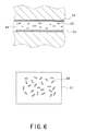
- FIG. 6 is a view schematically showing an alignment state of liquid crystal molecules at the time when a voltage is applied in a case where no alignment control mechanism is provided.
- FIG. 7 is a view schematically showing an alignment state of liquid crystal molecules at the time when a voltage is applied in a case where linear protrusions and openings that define alignment control mechanisms are provided.
- FIG. 8 is a magnified schematic plan view showing one pixel in a conventional liquid crystal display device.
- FIG. 9 is a cross-sectional view along the line C-C in FIG. 8 .
- FIG. 1 is a magnified schematic plan view showing one pixel in the liquid crystal display device according to the preferred embodiment of the present invention.
- FIG. 2 is a cross-sectional view along the line A-A in FIG. 1 .
- FIG. 3 is a cross-sectional view along the line B-B in FIG. 1
- a liquid crystal layer 40 is interposed between a pair of opposed glass substrates 10 and 30 ( 10 : the array substrate, 30: the color filter substrate), and on the glass substrate 10 which is located lower, pixel electrodes 17 are arranged in a matrix.
- a description of the glass substrate (array substrate) 10 is provided.
- a pair of gate bus lines 11 and a pair of source bus lines 12 preferably made from aluminum are formed to be perpendicular to each other.
- the gate bus lines 11 and the source bus lines 12 cross each other such that the gate bus lines 11 are located lower than the source bus lines 12 at intersection portions thereof, and the gate bus lines 11 and the source bus lines 12 are electrically insulated from each other at the intersection portions.
- a TFT (thin film transistor) 13 that defines a switching element is provided, to which a gate electrode 11 a that defines a part of the gate bus line 11 is connected.
- the gate bus line 11 and the gate electrode 11 a are formed in one wiring layer (a first wiring layer).
- the gate bus line 11 and the gate electrode 11 a are formed by patterning one conductive film.
- the gate bus line 11 and the gate electrode 11 a are coated with a gate insulating film 14 preferably made from silicon nitride (see FIG. 2 ).
- a semiconductor layer (not shown) preferably made from amorphous silicon is formed to be integral with the TFT 13 so as to overlay the gate electrode 11 a .
- a source electrode 13 a and a drain electrode 13 b are formed on both sides of the semiconductor layer on the gate electrode 11 a so as to be spaced apart from each other.
- the source electrode 13 a is connected to the source bus line 12
- the drain electrode 13 b is connected to the pixel electrode 17 via a contact hole 17 a .
- the source bus lines 12 , the source electrode 13 a and the drain electrode 13 b are formed in one wiring layer (a second wiring layer), which is not shown in FIG. 2 .
- the TFT 13 is on/off controlled by a scanning signal voltage provided by the gate electrode 11 a of the gate bus line 11 .
- a display signal voltage provided by the source electrode 13 a via the source bus line 12 is provided to the pixel electrode 17 via the drain electrode 13 b and the contact hole 17 a of the pixel electrode 17 .
- the source bus line 12 and the TFT 13 are coated with an interlayer insulating film 19 which is formed on the gate insulating film 14 .
- the interlayer insulating film 19 is preferably made from a photosensitive acrylic resin (photosensitive organic film) material, and is interposed between the TFT 13 and the first and second wiring layers (the gate bus line 11 and the source bus line 12 ), and the pixel electrode 17 in order to insulate the electric conductors from each other (see FIG. 2 ).
- the pixel electrode 17 is formed per pixel region.
- the pixel electrode 17 is preferably made from a transparent electric conductor such as an ITO (indium-tin oxide) material.
- the pixel electrode 17 having a substantially rectangular shape has four corner portions 17 b to 17 e , and among them, the upper left corner portion 17 b , the upper right corner portion 17 d and the lower right corner portion 17 e where a TFT 13 is not located are rounded.
- a plurality of openings 18 of slits are formed to extend in an oblique direction.
- the openings 18 are provided and arranged to generate an oblique electric field (a fringe field) at the time when a voltage is applied and to control liquid crystal molecule alignment in order to improve viewing angle characteristics.
- the openings 18 which are oblique at a given angle are arranged to be vertically symmetrical in each pixel electrode 17 as shown in FIG. 1 .
- a lower alignment layer 21 is formed on the pixel electrode 17 as shown in FIG. 2 .
- the lower alignment layer 21 is preferably made from a polyimide resin.
- a description of a method to manufacture the above-described glass substrate (array substrate) 10 will be provided.
- a single-layer or multi-layer conductor film made from materials such as tungsten, titanium, aluminum and chromium is formed on the glass substrate 10 .
- This conductor film can be formed by a known method such as sputtering.
- the formed conductor film is then formed into a predetermined pattern preferably by photolithography.
- the gate bus lines 11 and the gate electrodes 11 a in the predetermined pattern are formed.
- the gate insulating film 14 is preferably made from silicon nitride and is formed preferably by a plasma CVD method.
- the semiconductor layers (not shown) of the TFTs 13 , the source bus lines 12 , the source electrodes 13 a and the drain electrodes 13 b are formed.
- the semiconductor layers of the TFTs 13 are preferably made from n+ type amorphous silicon and are formed preferably by a plasma CVD method.
- the source bus lines 12 , the source electrodes 13 a and the drain electrodes 13 b are formed in the same manner as the gate bus lines 11 .
- the interlayer insulating film 19 made from a photosensitive acrylic resin (photosensitive organic film) material is formed, and contact holes are formed in the formed interlayer insulating film 19 preferably by photolithography.
- the transparent conductive film made from the TTO material is formed preferably by sputtering.
- the formed ITO film is then formed into a predetermined pattern preferably by photolithography.
- the pixel electrodes 17 and the contact holes 17 a in the predetermined pattern are formed.
- the lower alignment layer 21 is formed. Specifically, a liquid alignment material consisting of polyimide or other material is applied preferably by a cylinder printing press or an inkjet printing press, and is then baked by heating the substrate preferably using a baking system. Thus, the solid-state lower alignment layer 21 is formed on the pixel electrodes 17 .
- the glass substrate (array substrate) 10 is formed through the processes described above.
- the black matrix 31 is formed under the glass substrate 30 .
- the areas on the glass substrate 10 where the gate bus lines 11 , the source bus lines 12 and the TFT 13 are formed are arranged to be shielded from light by the black matrix 31 .
- a color layer 32 having one color among red (R), green (G), and blue (B) is formed in each pixel.
- the red (R), green (G), and blue (B) color layers 32 are repeatedly aligned in order in a horizontal direction, while the color layers 32 having the same color are aligned in a vertical direction.
- a common electrode 33 common to each pixel is formed.
- the common electrode 33 is also made from a transparent electric conductor such as an ITO material.
- linear protrusions 34 a , 34 b and 34 c are formed under the common electrode 33 .
- the linear protrusions 34 a to 34 c which are oblique at a given angle are arranged to be vertically symmetrical in each pixel electrode 17 .
- the linear protrusions 34 a to 34 c are provided and arranged to align liquid crystal molecules in given inclined directions relative to the vertical direction in order to improve viewing angle characteristics.
- an upper alignment layer 36 is formed to cover the linear protrusions 34 a and 34 b as shown in FIG. 2 .
- the upper alignment layer 36 is preferably made from a polyimide resin.
- a BM resist (a photosensitive resin composition including a black coloring agent) or other material is applied on the glass substrate 30 .
- the applied BM resist is formed into a predetermined pattern preferably by photolithography.
- the black matrix 31 in the predetermined pattern is formed.
- color inks made of a red, green and blue coloring photoresist materials are applied and formed into a predetermined pattern preferably by photolithography.
- the color layers 32 in the predetermined pattern are formed.
- the transparent conductive film made from the ITO material is formed using sputtering, and thus the common electrode 33 is formed.
- a resist (a photosensitive resin composition) or other material is applied on the common electrode 33 .
- the applied resist is formed into a predetermined pattern preferably by photolithography.
- the linear protrusions 34 a to 34 c in the predetermined pattern are formed.
- the upper alignment layer 36 is formed. Specifically, a liquid alignment material consisting of polyimide or other material is applied preferably by a cylinder printing press or an inkjet printing press, and is then baked by heating the substrate preferably using a baking system. Thus, the solid-state upper alignment layer 36 is formed on the common electrode 33 .
- the glass substrate (color filter substrate) 30 is formed through the processes described above.
- polarizing plates (not shown) are placed under the glass substrate 10 and on the glass substrate 30 . Transmission axes of the pair of polarizing plates are arranged to be substantially perpendicular to each other (crossed Nicols). The transmission axis of one of the polarizing plates is placed in the direction horizontal to a display surface, and is arranged to be oblique at about 45 degrees with respect to the extending directions of the openings 18 of slits and the linear protrusions 34 a to 34 c.
- a thermal-hardening or ultraviolet-cure sealing material and a common transfer material are applied to the substrate 10 or 30 preferably using a seal patterning device. Then, a liquid crystal is dropped filled in a display region on the substrate 10 or 30 preferably using a liquid crystal drop fill device, and the substrates 10 and 30 are bonded together in a reduced-pressure atmosphere to harden the sealing material.
- the liquid crystal display device 1 is prepared.
- FIG. 3 is a cross-sectional view along the line B-B in FIG. 1 .
- the linear protrusion 34 c is placed on the common electrode 33 at a position where the linear protrusion 34 c controls the alignment of the liquid crystal molecules 53 inside a position where the oblique electric field 59 which is generated at the edge of the corner portion 17 e of the pixel electrode 17 at the time when a voltage is applied between the electrodes 33 and 17 controls the alignment of the liquid crystal molecules 53 , so that the alignment control in the liquid crystal layer 40 is more excellent at the corner portion 17 e of the pixel electrode 17 than the case as shown in FIG. 9 .
- FIG. 4 is a table showing relations between overlapping widths W ( ⁇ m) of the linear protrusion 34 c with the corner portion 17 e shown in FIG. 1 , and evaluations of the alignment observed from a display screen. As shown in the table, when the overlapping width W is 0 ⁇ m, poor alignment is caused as described above and is rated as very unfavorable (X).
- the overlapping width W When the overlapping width W is 2 ⁇ m, poor alignment is slightly caused and is rated as unfavorable ( ⁇ ). When the overlapping width W is 4 ⁇ m, 6 ⁇ m or 8 ⁇ m, no poor alignment is caused and is rated as favorable ( ⁇ ), which means favorable alignment with no transmittance loss. Thus, it is apparent that by securing the overlapping width of 4 ⁇ m or more, the alignment control in the liquid crystal layer 40 becomes more favorable.
- FIG. 5 is a view showing a modified example of the pixel in the liquid crystal display device shown in FIG. 1 .
- auxiliary portions 35 which extend from the ends of the linear protrusions 34 c in the horizontal direction and the vertical direction in order to widen a region where the alignment of the liquid crystal molecules 53 is controlled inside the edges of the corner portions 17 d and 17 e of the pixel electrode 17 or in order to improve capability for the alignment control.
Applications Claiming Priority (3)
| Application Number | Priority Date | Filing Date | Title |
|---|---|---|---|
| JP2006-256781 | 2006-09-22 | ||
| JP2006256781 | 2006-09-22 | ||
| PCT/JP2007/057467 WO2008035471A1 (fr) | 2006-09-22 | 2007-04-03 | Dispositif d'affichage à cristaux liquides |
Related Parent Applications (1)
| Application Number | Title | Priority Date | Filing Date |
|---|---|---|---|
| PCT/JP2007/057467 A-371-Of-International WO2008035471A1 (fr) | 2006-09-22 | 2007-04-03 | Dispositif d'affichage à cristaux liquides |
Related Child Applications (1)
| Application Number | Title | Priority Date | Filing Date |
|---|---|---|---|
| US13/447,761 Continuation US8432520B2 (en) | 2006-09-22 | 2012-04-16 | Liquid crystal display device |
Publications (2)
| Publication Number | Publication Date |
|---|---|
| US20100060835A1 US20100060835A1 (en) | 2010-03-11 |
| US8159640B2 true US8159640B2 (en) | 2012-04-17 |
Family
ID=39200301
Family Applications (2)
| Application Number | Title | Priority Date | Filing Date |
|---|---|---|---|
| US12/441,445 Active 2027-12-27 US8159640B2 (en) | 2006-09-22 | 2007-04-03 | Liquid crystal display device |
| US13/447,761 Expired - Fee Related US8432520B2 (en) | 2006-09-22 | 2012-04-16 | Liquid crystal display device |
Family Applications After (1)
| Application Number | Title | Priority Date | Filing Date |
|---|---|---|---|
| US13/447,761 Expired - Fee Related US8432520B2 (en) | 2006-09-22 | 2012-04-16 | Liquid crystal display device |
Country Status (5)
| Country | Link |
|---|---|
| US (2) | US8159640B2 (fr) |
| EP (1) | EP2065754B1 (fr) |
| JP (1) | JPWO2008035471A1 (fr) |
| CN (1) | CN101517468B (fr) |
| WO (1) | WO2008035471A1 (fr) |
Cited By (1)
| Publication number | Priority date | Publication date | Assignee | Title |
|---|---|---|---|---|
| US8432520B2 (en) | 2006-09-22 | 2013-04-30 | Sharp Kabushiki Kaisha | Liquid crystal display device |
Families Citing this family (3)
| Publication number | Priority date | Publication date | Assignee | Title |
|---|---|---|---|---|
| JP2015072374A (ja) * | 2013-10-03 | 2015-04-16 | 株式会社ジャパンディスプレイ | 液晶表示装置 |
| US10768490B2 (en) * | 2018-06-27 | 2020-09-08 | Sharp Kabushiki Kaisha | Liquid crystal display device with patterned alignment layer for improved brightness |
| DE102019004521A1 (de) * | 2018-07-02 | 2020-01-02 | Sharp Kabushiki Kaisha | Aktivmatrixsubstrat und verfahren zur herstellung eines aktivmatrixsubstrats |
Citations (10)
| Publication number | Priority date | Publication date | Assignee | Title |
|---|---|---|---|---|
| JP2002229038A (ja) | 2001-02-06 | 2002-08-14 | Fujitsu Ltd | 液晶表示装置及び液晶配向方法 |
| JP2003043488A (ja) | 2001-08-02 | 2003-02-13 | Sanyo Electric Co Ltd | 液晶表示装置 |
| US6661488B1 (en) | 1997-06-12 | 2003-12-09 | Fujitsu Limited | Vertically-alligned (VA) liquid crystal display device |
| US6710837B1 (en) | 1998-05-16 | 2004-03-23 | Samsung Electronics Co., Ltd. | Liquid crystal displays having multi-domains and a manufacturing method thereof |
| US6879364B1 (en) | 1998-09-18 | 2005-04-12 | Fujitsu Display Technologies Corporation | Liquid crystal display apparatus having alignment control for brightness and response |
| US20060023149A1 (en) | 2004-07-30 | 2006-02-02 | Innolux Display Corp. | Continuous domain vertical alignment liquid crystal display |
| US20060092366A1 (en) | 1999-07-09 | 2006-05-04 | Hiroyasu Inoue | Liquid crystal display and method of fabricating the same |
| EP1666963A1 (fr) | 2004-12-03 | 2006-06-07 | Samsung Electronics Co., Ltd. | Panneau à réseau de transistors à couche mince pour un dispositif d'affichage à cristal liquide et procédé de fabrication correspondant |
| JP2006343775A (ja) | 2006-08-23 | 2006-12-21 | Sharp Corp | 液晶表示装置用基板及びその製造方法及びそれを備えた液晶表示装置 |
| US7218369B2 (en) * | 2003-10-15 | 2007-05-15 | Samsung Electronics Co., Ltd. | Liquid crystal display with notch formed in pixel electrode |
Family Cites Families (8)
| Publication number | Priority date | Publication date | Assignee | Title |
|---|---|---|---|---|
| JP2001324710A (ja) * | 2000-05-17 | 2001-11-22 | Nec Corp | 液晶表示装置およびその製造方法ならびに駆動方法 |
| KR100729762B1 (ko) * | 2000-11-14 | 2007-06-20 | 삼성전자주식회사 | 측면 대비비 및 측면 색재현성을 향상시킨 액정 표시 장치 |
| JP4104885B2 (ja) * | 2002-03-18 | 2008-06-18 | シャープ株式会社 | 液晶表示装置及びその製造方法 |
| JP3913653B2 (ja) * | 2002-09-30 | 2007-05-09 | 三洋電機株式会社 | 液晶表示装置 |
| JP2005055880A (ja) * | 2003-07-24 | 2005-03-03 | Sharp Corp | 液晶表示装置およびその駆動方法 |
| KR101112537B1 (ko) * | 2004-06-03 | 2012-02-29 | 삼성전자주식회사 | 다중 도메인 액정 표시 장치 및 그에 사용되는 표시판 |
| KR101112539B1 (ko) * | 2004-07-27 | 2012-02-15 | 삼성전자주식회사 | 다중 도메인 액정 표시 장치 및 그에 사용되는 표시판 |
| WO2008035471A1 (fr) | 2006-09-22 | 2008-03-27 | Sharp Kabushiki Kaisha | Dispositif d'affichage à cristaux liquides |
-
2007
- 2007-04-03 WO PCT/JP2007/057467 patent/WO2008035471A1/fr active Application Filing
- 2007-04-03 JP JP2008535268A patent/JPWO2008035471A1/ja active Pending
- 2007-04-03 EP EP07740903.5A patent/EP2065754B1/fr not_active Not-in-force
- 2007-04-03 US US12/441,445 patent/US8159640B2/en active Active
- 2007-04-03 CN CN2007800349839A patent/CN101517468B/zh not_active Expired - Fee Related
-
2012
- 2012-04-16 US US13/447,761 patent/US8432520B2/en not_active Expired - Fee Related
Patent Citations (15)
| Publication number | Priority date | Publication date | Assignee | Title |
|---|---|---|---|---|
| JP2006209143A (ja) | 1997-06-12 | 2006-08-10 | Sharp Corp | 液晶表示装置 |
| US7304703B1 (en) | 1997-06-12 | 2007-12-04 | Sharp Kabushiki Kaisha | Vertically-aligned (VA) liquid crystal display device |
| US6661488B1 (en) | 1997-06-12 | 2003-12-09 | Fujitsu Limited | Vertically-alligned (VA) liquid crystal display device |
| US6724452B1 (en) | 1997-06-12 | 2004-04-20 | Fujitsu Display Technologies Corporation | Vertically aligned (VA) liquid crystal display device |
| US20040119924A1 (en) | 1997-06-12 | 2004-06-24 | Fujitsu Display Technology Corporation | Vertically-aligned (VA) liquid crystal display device |
| US6710837B1 (en) | 1998-05-16 | 2004-03-23 | Samsung Electronics Co., Ltd. | Liquid crystal displays having multi-domains and a manufacturing method thereof |
| US6879364B1 (en) | 1998-09-18 | 2005-04-12 | Fujitsu Display Technologies Corporation | Liquid crystal display apparatus having alignment control for brightness and response |
| US20060092366A1 (en) | 1999-07-09 | 2006-05-04 | Hiroyasu Inoue | Liquid crystal display and method of fabricating the same |
| US20060098151A1 (en) | 1999-07-09 | 2006-05-11 | Hiroyasu Inoue | Liquid crystal display and method of fabricating the same |
| JP2002229038A (ja) | 2001-02-06 | 2002-08-14 | Fujitsu Ltd | 液晶表示装置及び液晶配向方法 |
| JP2003043488A (ja) | 2001-08-02 | 2003-02-13 | Sanyo Electric Co Ltd | 液晶表示装置 |
| US7218369B2 (en) * | 2003-10-15 | 2007-05-15 | Samsung Electronics Co., Ltd. | Liquid crystal display with notch formed in pixel electrode |
| US20060023149A1 (en) | 2004-07-30 | 2006-02-02 | Innolux Display Corp. | Continuous domain vertical alignment liquid crystal display |
| EP1666963A1 (fr) | 2004-12-03 | 2006-06-07 | Samsung Electronics Co., Ltd. | Panneau à réseau de transistors à couche mince pour un dispositif d'affichage à cristal liquide et procédé de fabrication correspondant |
| JP2006343775A (ja) | 2006-08-23 | 2006-12-21 | Sharp Corp | 液晶表示装置用基板及びその製造方法及びそれを備えた液晶表示装置 |
Non-Patent Citations (1)
| Title |
|---|
| International Search Report for PCT/JP2007/057467, mailed Jul. 3, 2007. |
Cited By (1)
| Publication number | Priority date | Publication date | Assignee | Title |
|---|---|---|---|---|
| US8432520B2 (en) | 2006-09-22 | 2013-04-30 | Sharp Kabushiki Kaisha | Liquid crystal display device |
Also Published As
| Publication number | Publication date |
|---|---|
| EP2065754A4 (fr) | 2010-01-06 |
| US20100060835A1 (en) | 2010-03-11 |
| JPWO2008035471A1 (ja) | 2010-01-28 |
| EP2065754B1 (fr) | 2014-03-26 |
| US8432520B2 (en) | 2013-04-30 |
| WO2008035471A1 (fr) | 2008-03-27 |
| US20120257153A1 (en) | 2012-10-11 |
| CN101517468A (zh) | 2009-08-26 |
| EP2065754A1 (fr) | 2009-06-03 |
| CN101517468B (zh) | 2011-01-19 |
Similar Documents
| Publication | Publication Date | Title |
|---|---|---|
| KR101427708B1 (ko) | 액정 표시 패널 | |
| JP3685795B2 (ja) | 液晶表示装置 | |
| KR100831229B1 (ko) | 고개구율 액정 표시 장치 | |
| JP5072952B2 (ja) | 液晶表示パネル、液晶表示装置及びテレビジョン受信機 | |
| US7538846B2 (en) | Liquid crystal display device and method of manufacturing the same | |
| JPH07199190A (ja) | 液晶表示装置 | |
| US20040150777A1 (en) | Liquid crystal display device | |
| US9835906B2 (en) | Liquid crystal display and method for manufacturing the same | |
| US8432520B2 (en) | Liquid crystal display device | |
| US10884292B2 (en) | Display device | |
| KR20000048876A (ko) | 액티브 매트릭스를 갖는 디스플레이 스크린 | |
| JP3819104B2 (ja) | 液晶表示装置 | |
| US10890815B2 (en) | Display apparatus | |
| US7898641B2 (en) | Production process of a display device, and a display device | |
| US9494838B2 (en) | Liquid crystal display device | |
| JP2010156805A (ja) | 液晶表示素子 | |
| US11003031B2 (en) | Display apparatus | |
| JP5525705B2 (ja) | 液晶表示装置 | |
| JP2001249352A (ja) | 液晶表示装置及びその製造方法 | |
| JP2005309293A (ja) | 液晶表示装置 | |
| JP2007271853A (ja) | 液晶表示装置 |
Legal Events
| Date | Code | Title | Description |
|---|---|---|---|
| AS | Assignment |
Owner name: SHARP KABUSHIKI KAISHA,JAPAN Free format text: ASSIGNMENT OF ASSIGNORS INTEREST;ASSIGNORS:INOUE, YUICHI;YAMAGUCHI, HIDEHIKO;SIGNING DATES FROM 20090305 TO 20090312;REEL/FRAME:023432/0691 Owner name: SHARP KABUSHIKI KAISHA, JAPAN Free format text: ASSIGNMENT OF ASSIGNORS INTEREST;ASSIGNORS:INOUE, YUICHI;YAMAGUCHI, HIDEHIKO;SIGNING DATES FROM 20090305 TO 20090312;REEL/FRAME:023432/0691 |
|
| STCF | Information on status: patent grant |
Free format text: PATENTED CASE |
|
| FEPP | Fee payment procedure |
Free format text: PAYOR NUMBER ASSIGNED (ORIGINAL EVENT CODE: ASPN); ENTITY STATUS OF PATENT OWNER: LARGE ENTITY |
|
| FPAY | Fee payment |
Year of fee payment: 4 |
|
| MAFP | Maintenance fee payment |
Free format text: PAYMENT OF MAINTENANCE FEE, 8TH YEAR, LARGE ENTITY (ORIGINAL EVENT CODE: M1552); ENTITY STATUS OF PATENT OWNER: LARGE ENTITY Year of fee payment: 8 |
|
| FEPP | Fee payment procedure |
Free format text: MAINTENANCE FEE REMINDER MAILED (ORIGINAL EVENT CODE: REM.); ENTITY STATUS OF PATENT OWNER: LARGE ENTITY |