US8088666B2 - Semiconductor device manufacture method including process of implanting impurity into gate electrode independently from source/drain and semiconductor device manufactured by the method - Google Patents
Semiconductor device manufacture method including process of implanting impurity into gate electrode independently from source/drain and semiconductor device manufactured by the method Download PDFInfo
- Publication number
- US8088666B2 US8088666B2 US11/898,830 US89883007A US8088666B2 US 8088666 B2 US8088666 B2 US 8088666B2 US 89883007 A US89883007 A US 89883007A US 8088666 B2 US8088666 B2 US 8088666B2
- Authority
- US
- United States
- Prior art keywords
- gate electrode
- film
- sidewall spacers
- implanted
- semiconductor substrate
- Prior art date
- Legal status (The legal status is an assumption and is not a legal conclusion. Google has not performed a legal analysis and makes no representation as to the accuracy of the status listed.)
- Expired - Fee Related, expires
Links
- 239000012535 impurity Substances 0.000 title claims abstract description 83
- 239000004065 semiconductor Substances 0.000 title claims abstract description 59
- 238000000034 method Methods 0.000 title claims description 43
- 238000004519 manufacturing process Methods 0.000 title claims description 18
- 239000000758 substrate Substances 0.000 claims abstract description 70
- 239000002344 surface layer Substances 0.000 claims abstract description 38
- 125000006850 spacer group Chemical group 0.000 claims description 68
- 239000011810 insulating material Substances 0.000 claims description 14
- 238000000926 separation method Methods 0.000 claims description 13
- 229910021332 silicide Inorganic materials 0.000 claims description 9
- FVBUAEGBCNSCDD-UHFFFAOYSA-N silicide(4-) Chemical compound [Si-4] FVBUAEGBCNSCDD-UHFFFAOYSA-N 0.000 claims description 9
- 238000005530 etching Methods 0.000 claims description 8
- 238000009826 distribution Methods 0.000 claims description 4
- 239000002184 metal Substances 0.000 claims description 4
- 229910052751 metal Inorganic materials 0.000 claims description 4
- 239000000463 material Substances 0.000 claims description 2
- 239000007943 implant Substances 0.000 claims 1
- 239000010408 film Substances 0.000 description 132
- 150000002500 ions Chemical class 0.000 description 58
- 238000005468 ion implantation Methods 0.000 description 41
- 229910052581 Si3N4 Inorganic materials 0.000 description 33
- VYPSYNLAJGMNEJ-UHFFFAOYSA-N Silicium dioxide Chemical compound O=[Si]=O VYPSYNLAJGMNEJ-UHFFFAOYSA-N 0.000 description 33
- HQVNEWCFYHHQES-UHFFFAOYSA-N silicon nitride Chemical compound N12[Si]34N5[Si]62N3[Si]51N64 HQVNEWCFYHHQES-UHFFFAOYSA-N 0.000 description 33
- 229910052814 silicon oxide Inorganic materials 0.000 description 33
- 239000010410 layer Substances 0.000 description 21
- XUIMIQQOPSSXEZ-UHFFFAOYSA-N Silicon Chemical compound [Si] XUIMIQQOPSSXEZ-UHFFFAOYSA-N 0.000 description 17
- 229910052710 silicon Inorganic materials 0.000 description 17
- 239000010703 silicon Substances 0.000 description 17
- 230000001133 acceleration Effects 0.000 description 16
- KRHYYFGTRYWZRS-UHFFFAOYSA-N Fluorane Chemical compound F KRHYYFGTRYWZRS-UHFFFAOYSA-N 0.000 description 13
- 238000010438 heat treatment Methods 0.000 description 12
- 238000005229 chemical vapour deposition Methods 0.000 description 10
- 238000009792 diffusion process Methods 0.000 description 10
- 229910021420 polycrystalline silicon Inorganic materials 0.000 description 9
- 229920005591 polysilicon Polymers 0.000 description 9
- 229910052796 boron Inorganic materials 0.000 description 7
- 229910017052 cobalt Inorganic materials 0.000 description 7
- 239000010941 cobalt Substances 0.000 description 7
- GUTLYIVDDKVIGB-UHFFFAOYSA-N cobalt atom Chemical compound [Co] GUTLYIVDDKVIGB-UHFFFAOYSA-N 0.000 description 7
- 229910052757 nitrogen Inorganic materials 0.000 description 6
- ZOXJGFHDIHLPTG-UHFFFAOYSA-N Boron Chemical compound [B] ZOXJGFHDIHLPTG-UHFFFAOYSA-N 0.000 description 5
- BHEPBYXIRTUNPN-UHFFFAOYSA-N hydridophosphorus(.) (triplet) Chemical compound [PH] BHEPBYXIRTUNPN-UHFFFAOYSA-N 0.000 description 4
- 238000010884 ion-beam technique Methods 0.000 description 4
- 238000000137 annealing Methods 0.000 description 3
- QPJSUIGXIBEQAC-UHFFFAOYSA-N n-(2,4-dichloro-5-propan-2-yloxyphenyl)acetamide Chemical compound CC(C)OC1=CC(NC(C)=O)=C(Cl)C=C1Cl QPJSUIGXIBEQAC-UHFFFAOYSA-N 0.000 description 3
- 238000000059 patterning Methods 0.000 description 3
- 229910052698 phosphorus Inorganic materials 0.000 description 3
- 239000010409 thin film Substances 0.000 description 3
- IJGRMHOSHXDMSA-UHFFFAOYSA-N Atomic nitrogen Chemical compound N#N IJGRMHOSHXDMSA-UHFFFAOYSA-N 0.000 description 2
- NBIIXXVUZAFLBC-UHFFFAOYSA-N Phosphoric acid Chemical compound OP(O)(O)=O NBIIXXVUZAFLBC-UHFFFAOYSA-N 0.000 description 2
- 238000000151 deposition Methods 0.000 description 2
- 230000000694 effects Effects 0.000 description 2
- 238000004151 rapid thermal annealing Methods 0.000 description 2
- 230000003213 activating effect Effects 0.000 description 1
- 230000002411 adverse Effects 0.000 description 1
- 229910000147 aluminium phosphate Inorganic materials 0.000 description 1
- 229910021417 amorphous silicon Inorganic materials 0.000 description 1
- 229910052785 arsenic Inorganic materials 0.000 description 1
- RQNWIZPPADIBDY-UHFFFAOYSA-N arsenic atom Chemical compound [As] RQNWIZPPADIBDY-UHFFFAOYSA-N 0.000 description 1
- HAYXDMNJJFVXCI-UHFFFAOYSA-N arsenic(5+) Chemical class [As+5] HAYXDMNJJFVXCI-UHFFFAOYSA-N 0.000 description 1
- QVGXLLKOCUKJST-UHFFFAOYSA-N atomic oxygen Chemical compound [O] QVGXLLKOCUKJST-UHFFFAOYSA-N 0.000 description 1
- 150000001638 boron Chemical class 0.000 description 1
- 238000005137 deposition process Methods 0.000 description 1
- 239000011521 glass Substances 0.000 description 1
- 230000010354 integration Effects 0.000 description 1
- 238000002955 isolation Methods 0.000 description 1
- 230000000873 masking effect Effects 0.000 description 1
- 238000012986 modification Methods 0.000 description 1
- 230000004048 modification Effects 0.000 description 1
- 239000012299 nitrogen atmosphere Substances 0.000 description 1
- 230000001590 oxidative effect Effects 0.000 description 1
- 229910052760 oxygen Inorganic materials 0.000 description 1
- 239000001301 oxygen Substances 0.000 description 1
- 230000003071 parasitic effect Effects 0.000 description 1
- 238000001020 plasma etching Methods 0.000 description 1
- 238000005498 polishing Methods 0.000 description 1
- 238000002203 pretreatment Methods 0.000 description 1
- 238000004528 spin coating Methods 0.000 description 1
- 239000000126 substance Substances 0.000 description 1
Images


Classifications
-
- H—ELECTRICITY
- H01—ELECTRIC ELEMENTS
- H01L—SEMICONDUCTOR DEVICES NOT COVERED BY CLASS H10
- H01L29/00—Semiconductor devices adapted for rectifying, amplifying, oscillating or switching, or capacitors or resistors with at least one potential-jump barrier or surface barrier, e.g. PN junction depletion layer or carrier concentration layer; Details of semiconductor bodies or of electrodes thereof ; Multistep manufacturing processes therefor
- H01L29/66—Types of semiconductor device ; Multistep manufacturing processes therefor
- H01L29/66007—Multistep manufacturing processes
- H01L29/66075—Multistep manufacturing processes of devices having semiconductor bodies comprising group 14 or group 13/15 materials
- H01L29/66227—Multistep manufacturing processes of devices having semiconductor bodies comprising group 14 or group 13/15 materials the devices being controllable only by the electric current supplied or the electric potential applied, to an electrode which does not carry the current to be rectified, amplified or switched, e.g. three-terminal devices
- H01L29/66409—Unipolar field-effect transistors
- H01L29/66477—Unipolar field-effect transistors with an insulated gate, i.e. MISFET
- H01L29/6653—Unipolar field-effect transistors with an insulated gate, i.e. MISFET using the removal of at least part of spacer, e.g. disposable spacer
-
- H—ELECTRICITY
- H01—ELECTRIC ELEMENTS
- H01L—SEMICONDUCTOR DEVICES NOT COVERED BY CLASS H10
- H01L21/00—Processes or apparatus adapted for the manufacture or treatment of semiconductor or solid state devices or of parts thereof
- H01L21/02—Manufacture or treatment of semiconductor devices or of parts thereof
- H01L21/04—Manufacture or treatment of semiconductor devices or of parts thereof the devices having at least one potential-jump barrier or surface barrier, e.g. PN junction, depletion layer or carrier concentration layer
- H01L21/18—Manufacture or treatment of semiconductor devices or of parts thereof the devices having at least one potential-jump barrier or surface barrier, e.g. PN junction, depletion layer or carrier concentration layer the devices having semiconductor bodies comprising elements of Group IV of the Periodic System or AIIIBV compounds with or without impurities, e.g. doping materials
- H01L21/28—Manufacture of electrodes on semiconductor bodies using processes or apparatus not provided for in groups H01L21/20 - H01L21/268
- H01L21/28008—Making conductor-insulator-semiconductor electrodes
- H01L21/28017—Making conductor-insulator-semiconductor electrodes the insulator being formed after the semiconductor body, the semiconductor being silicon
- H01L21/28026—Making conductor-insulator-semiconductor electrodes the insulator being formed after the semiconductor body, the semiconductor being silicon characterised by the conductor
- H01L21/28035—Making conductor-insulator-semiconductor electrodes the insulator being formed after the semiconductor body, the semiconductor being silicon characterised by the conductor the final conductor layer next to the insulator being silicon, e.g. polysilicon, with or without impurities
-
- H—ELECTRICITY
- H01—ELECTRIC ELEMENTS
- H01L—SEMICONDUCTOR DEVICES NOT COVERED BY CLASS H10
- H01L21/00—Processes or apparatus adapted for the manufacture or treatment of semiconductor or solid state devices or of parts thereof
- H01L21/70—Manufacture or treatment of devices consisting of a plurality of solid state components formed in or on a common substrate or of parts thereof; Manufacture of integrated circuit devices or of parts thereof
- H01L21/77—Manufacture or treatment of devices consisting of a plurality of solid state components or integrated circuits formed in, or on, a common substrate
- H01L21/78—Manufacture or treatment of devices consisting of a plurality of solid state components or integrated circuits formed in, or on, a common substrate with subsequent division of the substrate into plural individual devices
- H01L21/82—Manufacture or treatment of devices consisting of a plurality of solid state components or integrated circuits formed in, or on, a common substrate with subsequent division of the substrate into plural individual devices to produce devices, e.g. integrated circuits, each consisting of a plurality of components
- H01L21/822—Manufacture or treatment of devices consisting of a plurality of solid state components or integrated circuits formed in, or on, a common substrate with subsequent division of the substrate into plural individual devices to produce devices, e.g. integrated circuits, each consisting of a plurality of components the substrate being a semiconductor, using silicon technology
- H01L21/8232—Field-effect technology
- H01L21/8234—MIS technology, i.e. integration processes of field effect transistors of the conductor-insulator-semiconductor type
- H01L21/8238—Complementary field-effect transistors, e.g. CMOS
- H01L21/823814—Complementary field-effect transistors, e.g. CMOS with a particular manufacturing method of the source or drain structures, e.g. specific source or drain implants or silicided source or drain structures or raised source or drain structures
-
- H—ELECTRICITY
- H01—ELECTRIC ELEMENTS
- H01L—SEMICONDUCTOR DEVICES NOT COVERED BY CLASS H10
- H01L21/00—Processes or apparatus adapted for the manufacture or treatment of semiconductor or solid state devices or of parts thereof
- H01L21/70—Manufacture or treatment of devices consisting of a plurality of solid state components formed in or on a common substrate or of parts thereof; Manufacture of integrated circuit devices or of parts thereof
- H01L21/77—Manufacture or treatment of devices consisting of a plurality of solid state components or integrated circuits formed in, or on, a common substrate
- H01L21/78—Manufacture or treatment of devices consisting of a plurality of solid state components or integrated circuits formed in, or on, a common substrate with subsequent division of the substrate into plural individual devices
- H01L21/82—Manufacture or treatment of devices consisting of a plurality of solid state components or integrated circuits formed in, or on, a common substrate with subsequent division of the substrate into plural individual devices to produce devices, e.g. integrated circuits, each consisting of a plurality of components
- H01L21/822—Manufacture or treatment of devices consisting of a plurality of solid state components or integrated circuits formed in, or on, a common substrate with subsequent division of the substrate into plural individual devices to produce devices, e.g. integrated circuits, each consisting of a plurality of components the substrate being a semiconductor, using silicon technology
- H01L21/8232—Field-effect technology
- H01L21/8234—MIS technology, i.e. integration processes of field effect transistors of the conductor-insulator-semiconductor type
- H01L21/8238—Complementary field-effect transistors, e.g. CMOS
- H01L21/823828—Complementary field-effect transistors, e.g. CMOS with a particular manufacturing method of the gate conductors, e.g. particular materials, shapes
- H01L21/823842—Complementary field-effect transistors, e.g. CMOS with a particular manufacturing method of the gate conductors, e.g. particular materials, shapes gate conductors with different gate conductor materials or different gate conductor implants, e.g. dual gate structures
-
- H—ELECTRICITY
- H01—ELECTRIC ELEMENTS
- H01L—SEMICONDUCTOR DEVICES NOT COVERED BY CLASS H10
- H01L29/00—Semiconductor devices adapted for rectifying, amplifying, oscillating or switching, or capacitors or resistors with at least one potential-jump barrier or surface barrier, e.g. PN junction depletion layer or carrier concentration layer; Details of semiconductor bodies or of electrodes thereof ; Multistep manufacturing processes therefor
- H01L29/66—Types of semiconductor device ; Multistep manufacturing processes therefor
- H01L29/66007—Multistep manufacturing processes
- H01L29/66075—Multistep manufacturing processes of devices having semiconductor bodies comprising group 14 or group 13/15 materials
- H01L29/66227—Multistep manufacturing processes of devices having semiconductor bodies comprising group 14 or group 13/15 materials the devices being controllable only by the electric current supplied or the electric potential applied, to an electrode which does not carry the current to be rectified, amplified or switched, e.g. three-terminal devices
- H01L29/66409—Unipolar field-effect transistors
- H01L29/66477—Unipolar field-effect transistors with an insulated gate, i.e. MISFET
- H01L29/6656—Unipolar field-effect transistors with an insulated gate, i.e. MISFET using multiple spacer layers, e.g. multiple sidewall spacers
-
- H—ELECTRICITY
- H01—ELECTRIC ELEMENTS
- H01L—SEMICONDUCTOR DEVICES NOT COVERED BY CLASS H10
- H01L29/00—Semiconductor devices adapted for rectifying, amplifying, oscillating or switching, or capacitors or resistors with at least one potential-jump barrier or surface barrier, e.g. PN junction depletion layer or carrier concentration layer; Details of semiconductor bodies or of electrodes thereof ; Multistep manufacturing processes therefor
- H01L29/66—Types of semiconductor device ; Multistep manufacturing processes therefor
- H01L29/66007—Multistep manufacturing processes
- H01L29/66075—Multistep manufacturing processes of devices having semiconductor bodies comprising group 14 or group 13/15 materials
- H01L29/66227—Multistep manufacturing processes of devices having semiconductor bodies comprising group 14 or group 13/15 materials the devices being controllable only by the electric current supplied or the electric potential applied, to an electrode which does not carry the current to be rectified, amplified or switched, e.g. three-terminal devices
- H01L29/66409—Unipolar field-effect transistors
- H01L29/66477—Unipolar field-effect transistors with an insulated gate, i.e. MISFET
- H01L29/66568—Lateral single gate silicon transistors
- H01L29/66575—Lateral single gate silicon transistors where the source and drain or source and drain extensions are self-aligned to the sides of the gate
- H01L29/6659—Lateral single gate silicon transistors where the source and drain or source and drain extensions are self-aligned to the sides of the gate with both lightly doped source and drain extensions and source and drain self-aligned to the sides of the gate, e.g. lightly doped drain [LDD] MOSFET, double diffused drain [DDD] MOSFET
Definitions
- the present invention relates to a semiconductor device and its manufacture method, and more particularly to a method of manufacturing a MOS FET whose gate electrode, source and drain regions are implanted with impurities and a semiconductor device fabricated by such a method.
- Polysilicon or amorphous silicon is used as the material of the gate electrode of a MOSFET. Impurities are implanted into a gate electrode either by implanting p- or n-type impurities into a silicon film to be used as the gate electrode before the silicon film is patterned or by patterning a silicon film and thereafter implanting impurities into the source and drain regions and the gate electrode at the same time.
- FIG. 5A shows examples of the cross sectional shape of a gate electrode.
- An element separation insulating film 501 is formed in the surface layer of a silicon substrate 500 .
- Gate electrodes 502 and 503 are formed in active regions defined by the element separation insulating film 501 .
- the gate electrodes 502 and 503 are formed by patterning a silicon film without annealing the phosphorous (P) and boron (B) implanted areas of the silicon film.
- the silicon film implanted with boron and patterned can form the gate electrode 503 having generally a rectangular shape.
- the silicon film implanted with phosphorous and patterned forms the gate electrode 502 having a cross sectional shape with its middle region being constricted.
- FIG. 5B is a cross sectional view of a gate electrode formed by implanting impurities into a silicon film and annealing before the film is patterned.
- a gate electrode 503 A having a rectangular cross section can be obtained, whereas in the area where phosphorous was implanted, the cross sectional shape of a gate electrode 502 A is likely to have a trapezoidal shape with a bell-bottom.
- Variations of the cross sectional shape raise no serious problem if a minimum processing size is relatively large.
- a silicon oxide film or a silicon oxynitride film formed on the surface of a gate electrode is very thin. If there are variations of the cross sectional shape of a gate electrode, it is difficult to form a very thin film with good reproductivity.
- impurities are implanted into source and drain regions and a gate electrode at the same time, it is not possible to independently control the impurity concentrations of the source and drain regions and the gate electrode.
- the dose of the source and drain regions is also 7 ⁇ 10 15 cm ⁇ 2 .
- the source and drain regions extend just under the gate electrode so that the influence of short channel effects becomes high.
- An object of this invention is to provide a semiconductor device manufacturing method capable of reducing variations of the cross sectional shape of a gate electrode and setting the impurity concentration of the gate electrode independently from that of the source and drain regions.
- Another object of the invention is to provide a semiconductor device manufactured by such a semiconductor device manufacturing method.
- a method of manufacturing a semiconductor device comprising: (a) a step of forming a gate electrode comprising semiconductor over a partial surface area of a semiconductor substrate; (b) a step of forming a mask member over a surface of the semiconductor substrate in an area adjacent to the gate electrode; (c) a step of implanting impurities into the gate electrode; (d) a step of removing the mask member; and (e) a step of implanting impurities into a surface layer of the semiconductor substrate on both sides of the gate electrode to form source and drain regions.
- the impurities are implanted by covering the surface of the semiconductor substrate with a mask member, the impurities can be implanted only into the gate electrode without implanting the impurities in the surface layer (source and drain regions) of the semiconductor substrate.
- a semiconductor device having the structure as defined in the following can be manufactured.
- a semiconductor device comprising: a semiconductor substrate; a gate insulating film made of a first insulating material and formed on a partial surface area of the semiconductor substrate; a gate electrode formed on the gate insulating film; first films made of a second insulating material and covering sidewalls of the gate electrode and first areas of the semiconductor substrate continuous with the sidewalls of the gate electrode, the first films being conformal to an underlying surface; second films made of a third insulating material and covering surfaces of the first films, the second films being conformal to the surfaces of the first films; sidewall spacers made of a fourth insulating material and disposed over the second films; extension regions of a first conductivity type disposed in a surface layer of the semiconductor substrate corresponding to the first areas; source and drain regions of the first conductivity type disposed in the surface layer of the semiconductor substrate corresponding to second areas outside of the first areas relative to the gate electrode; and high impurity concentration regions having an impurity concentration higher than an impurity concentration of
- a method of manufacturing a semiconductor device comprising the steps of: (i) forming a gate electrode consisting of semiconductor over a partial surface area of a semiconductor substrate; (j) implanting impurities into a surface layer of the semiconductor substrate by using said gate electrode as a mask; (k) forming first sidewall spacers consisting of insulating material on sidewalls of said gate electrode; (l) implanting impurities into the surface layer of the semiconductor substrate by using said gate electrode and said first sidewall spacers as a mask; (m) forming second sidewall spacers consisting of insulating material on sidewalls of said first sidewall spacers; (n) implanting impurities into said gate electrode; and (o) performing a heat treatment to activate the implanted impurities.
- Impurities can be implanted into the gate electrode without implanting the extension regions, source and drain regions below the first and the second sidewall spacers because the first and the second sidewall spacers are formed on the sidewall of the gate electrode.
- a semiconductor device comprising: a semiconductor substrate; a gate insulating film consisting of first insulating material formed on a partial surface area of said semiconductor substrate; a gate electrode formed on said gate insulating film; impurity diffusion regions formed in a surface layer of said semiconductor substrate on both sides of said gate electrode, each of said impurity diffusion regions including a first region, a second region deeper than the first region, and a third region deeper than the second region in this order from said gate electrode; sidewall spacers formed on sidewalls of said gate electrode and reaching halfway an upper surface of the second region; and a metal silicide film formed on an upper surface of the second region not covered with said sidewall spacer and on a surface of the third region.
- a gate electrode is patterned prior to implanting impurities into a semiconductor layer. It is therefore possible to reduce variations of the cross sectional shape of a gate electrode.
- FIGS. 1A to 1O are cross sectional views of a substrate illustrating a semiconductor device manufacturing method according to a first embodiment of the invention.
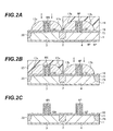
- FIGS. 2A to 2N are cross sectional views of a substrate illustrating a semiconductor device manufacturing method according to a second embodiment of the invention.
- FIGS. 3A to 3M are cross sectional views of a substrate illustrating a semiconductor device manufacturing method according to a third embodiment of the invention.
- FIG. 4A to 4H are cross sectional views of a substrate illustrating a semiconductor device manufacturing method according to a fourth embodiment of the invention.
- FIGS. 5A and 5B are cross sectional views showing examples of a gate electrode formed by a prior art method.
- FIGS. 1A to 1O a semiconductor device manufacturing method according to the first embodiment of the invention will be described.
- an element separation insulating film 2 of silicon oxide is formed by known shallow trench isolation technique. Active regions are defined by the element separation insulating film 2 .
- a p-type well 3 is formed in the area where an n-channel MOS FET is to be formed, and an n-type well 4 is formed in the area where a p-channel MOSFET is to be formed.
- a silicon oxynitride (SiON) film having a thickness of 1.2 nm is formed on the surface of the substrate 1 .
- the SiON film is formed by forming a silicon oxide film by thermally oxidizing the surface of the substrate 1 and thereafter annealing the silicon oxide film in a nitrogen atmosphere.
- a non-doped polysilicon film having a thickness of 110 nm is formed by chemical vapor deposition (CVD).
- the surface of the polysilicon film is covered with a resist pattern to etch the polysilicon film.
- a gate electrode 6 N made of polysilicon is left, and on the surface of the n-type well 4 , a gate electrode 6 P made of polysilicon is left.
- Etching the polysilicon film may be performed by reactive ion etching using HBr and O 2 .
- the gate length is, for example, 40 to 100 nm. Since impurity is not implanted in the polysilicon film, it is possible to suppress variations of the cross sectional shapes of the gate electrodes 6 N and 6 P.
- the resist pattern is removed. At this time, the SiON film not covered with the gate electrodes 6 N and 6 P is removed.
- the area where the n-type well 4 is formed is covered with a resist pattern 7 .
- the gate electrode 6 N As shown in FIG. 1B , the area where the n-type well 4 is formed is covered with a resist pattern 7 .
- arsenic (As) ions are implanted into a surface layer of the p-type well 3 under the conditions of an acceleration energy of 5 keV and a dose of 1 ⁇ 10 15 cm ⁇ 2 .
- An ion beam is inclined from the substrate normal direction toward the gate length direction (carrier motion direction) and has an incidence angle of 0 to 7°. This arsenic ion implantation forms n-type extension regions 8 N of the source and drain regions.
- boron (B) ions are implanted into the surface layer of the p-type well 3 under the conditions of an acceleration energy of 9 keV and a dose of 4 ⁇ 10 14 cm ⁇ 2 .
- An ion beam is inclined from the substrate normal direction toward the gate length direction and has an incidence angle of 15 to 30°. This boron ion implantation forms p-type pocket regions 9 N. After ion implantation, the resist pattern 7 is removed.
- the area where the p-type well 3 is formed is covered with a resist pattern 11 .
- B ions are implanted into a surface layer of the n-type well 4 under the conditions of an acceleration energy of 0.5 keV and a dose of 8 ⁇ 10 14 cm ⁇ 2 .
- An ion beam is inclined from the substrate normal direction toward the gate length direction and has an incidence angle of 0 to 7°. This B ion implantation forms p-type extension regions 8 P of the source and drain regions.
- As ions are implanted into the surface layer of the n-type well 4 under the conditions of an acceleration energy of 60 keV and a dose of 4 ⁇ 10 14 cm ⁇ 2 .
- An ion beam is inclined from the substrate normal direction toward the gate length direction and has an incidence angle of 15 to 30°. This As ion implantation forms n-type pocket regions 9 P. After ion implantation, the resist pattern 11 is removed.
- a silicon oxide film 15 having a thickness of 10 to 20 nm is formed on or over the surfaces of the gate electrodes 6 N and 6 P and substrate 1 by CVD.
- a silicon nitride film 16 having a thickness of 20 nm is formed by CVD.
- a thick silicon oxide film 17 having a thickness of 100 to 300 nm is formed by CVD.
- the thick silicon oxide film 17 is anisotropically etched to leave a mask member 17 a of silicon oxide on the sidewalls of the gate electrode 6 N and a mask member 17 b of silicon oxide on the sidewalls of the gate electrode 6 P.
- the mask member 17 a is disposed on or over a ring area surrounding the gate electrode 6 N of the surface of the substrate 1 .
- the mask member 17 b is disposed on a ring area surrounding the gate electrode 6 P of the surface of the substrate 1 .
- the area where the n-type well 4 is formed is covered with a resist pattern 19 .
- P ions are implanted into the gate electrode 6 N under the conditions of acceleration energy of 8 keV and a dose of 7 ⁇ 10 15 cm ⁇ 2 . Since the substrate surface layer near the gate electrode 6 N is covered with the mask member 17 a , P ions are not implanted into the substrate surface layer near the gate electrode.
- a high impurity concentration region 20 doped with P ions is formed. After P ions are implanted, the resist pattern 19 is removed.
- the area where the p-type well 3 is formed is covered with a resist pattern 23 .
- B ions are implanted into the gate electrode 6 P under the conditions of acceleration energy of 3 keV and a dose of 4 ⁇ 10 15 cm ⁇ 2 . Since the substrate surface layer near the gate electrode 6 P is covered with the mask member 17 b , B ions are not implanted into the substrate surface layer near the gate electrode.
- a high impurity concentration region 24 doped with B ions is formed. After B ions are implanted, the resist pattern 23 is removed.
- the mask members 17 a and 17 b shown in FIG. 1H are removed by hydrofluoric acid (HF). Since the element separation insulating film 2 of silicon oxide is covered with the silicon nitride film 16 , the surface layer of the element separation insulating film 2 can be prevented from being etched by HF.
- HF hydrofluoric acid
- an insulating film 26 of silicon oxide is deposited to a thickness of 80 nm by CVD.
- This insulating film 26 may be made of silicon nitride.
- the silicon oxide film 15 , silicon nitride film 16 and insulating film 26 shown in FIG. 1J are anisotropically etched. As viewed along a direction in parallel to the substrate normal, a silicon oxide film 15 N is left in a ring area adjacent to and surrounding the gate electrode 6 N and on the sidewalls of the gate electrode 6 N. The silicon oxide film 15 N is conformal to the underlying surface.
- a silicon nitride film 16 N is left on the surface of the silicon oxide film 15 N.
- the silicon nitride film 16 N is also conformal to the underlying surface.
- sidewall spacers 26 N of silicon oxide are left on the surface of the silicon nitride film 16 N.
- a silicon oxide film 15 P, a silicon nitride film 16 P and sidewall spacers 26 P are left.
- the area where the n-type well 4 is formed is covered with a resist pattern 30 .
- P ions are implanted into the surface layer of the p-type well 3 under the conditions of an acceleration energy of 8 keV and a dose of 2 ⁇ 10 15 cm ⁇ 2 .
- P ion implantation forms source and drain regions 31 N.
- P ions are also implanted into the gate electrode 6 N.
- a total dose of P ions into the gate electrode 6 N is therefore 9 ⁇ 10 15 cm ⁇ 2 .
- the resist pattern 30 is removed.
- the area where the p-type well 3 is formed is covered with a resist pattern 34 .
- B ions are implanted into the surface layer of the n-type well 4 under the conditions of an acceleration energy of 3 keV and a dose of 2 ⁇ 10 15 cm ⁇ 2 .
- P ion implantation forms source and drain regions 31 P.
- B ions are also implanted into the gate electrode 6 P.
- a total dose of B ions into the gate electrode 6 P is therefore 6 ⁇ 10 15 cm ⁇ 2 .
- the resist pattern 34 shown in FIG. 1M is removed.
- a heat treatment is performed for 3 seconds at 1050° C. to activate implanted impurity ions.
- a cobalt (Co) film is formed on the surfaces of the gate electrodes 6 N and 6 P, sidewall spacers 26 N and 26 P and substrate 1 .
- a heat treatment is performed to proceed a silicide reaction between the Co film and silicon.
- a cobalt silicide (CoSi) film 33 N is therefore formed on the surfaces of the source and drain regions 31 N and n-type high impurity concentration region 20 , and a CoSi film 34 N is formed on the upper surface of the gate electrode 6 N.
- a cobalt silicide (CoSi 2 ) film 33 P is formed on the surfaces of the source and drain regions 31 P and p-type high impurity concentration region 24 , and a CoSi 2 film 34 P is formed on the upper surface of the gate electrode 6 P. After the silicide reaction, an unreacted Co film is removed.
- ions are implanted into the gate electrodes 6 N and 6 P.
- the source and drain regions are maintained covered with the mask members 17 a and 17 b , although the impurities are implanted into the gate electrodes 6 N and 6 P, they are not implanted into the source and drain regions. It is therefore possible to set the impurity concentration of the gate electrodes 6 N and 6 P independently from that of the source and drain regions.
- these high impurity concentration regions 20 and 24 in the areas not covered with the mask members 17 a and 17 b are formed, these high impurity concentration regions are sufficiently remote from the gate electrodes 6 N and 6 P so that the operation of MOSFETs are not adversely affected.
- the sidewalls of the gate electrodes 6 N and 6 P are covered with the silicon oxide films 15 N and 15 P as shown in FIG. 1O . Since the dielectric constant of silicon oxide is lower than that of silicon nitride, parasitic capacitance between the gate electrode 6 N and extension regions 8 N and between the gate electrode 6 P and extension regions 8 P can be reduced more than the case wherein the silicon nitride films 16 N and 16 P are in direct contact with the sidewalls of the gate electrodes 6 N and 6 P.
- the processes up to the state shown in FIG. 2A will be described.
- the structure shown in FIG. 2A corresponds to the structure shown in FIG. 1G of the first embodiment with the extension regions 8 N and 8 P and pocket regions 9 N and 9 P being removed.
- the structure shown in FIG. 2A can be formed by omitting the ion implantation process shown in FIG. 1B for forming the extension regions 8 N and pocket regions 9 N and the ion implantation process shown in FIG. 1C for forming the extension regions 8 P and pocket regions 9 P. Similar to the first embodiment, after P ions are implanted into the gate electrode 6 N, the resist pattern 19 is removed.
- the area where the p-type well 3 is formed is covered with a resist pattern 23 , and B ions are implanted into the gate electrode 6 P.
- the ion implantation conditions are the same as those for B ions of the first embodiment described with FIG. 1H . After B ions are implanted, the resist pattern 23 is removed.
- the mask members 17 a and 17 b shown in FIG. 2B are removed by hydrofluoric acid (HF). Since the element separation insulating film 2 of silicon oxide is covered with the silicon nitride film 16 , the surface layer of the element separation insulating film 2 is prevented from being etched by hydrofluoric acid.
- HF hydrofluoric acid
- a silicon nitride film 40 is deposited on or over the silicon nitride film 16 to a thickness of 80 nm by CVD.
- the silicon nitride films 40 and 16 shown in FIG. 2D are anisotropically etched to leave silicon nitride films 16 N and 40 N on the sidewalls of the gate electrode 6 N and silicon nitride films 16 P and 40 P on the sidewalls of the gate electrode 6 P.
- the silicon nitride films 40 N and 40 P are disposed on or over the surface of the substrate 1 in an area narrower than the area where the mask members 17 a and 17 b shown in FIG. 2A are disposed.
- the area where the n-type well 4 is formed is covered with a resist pattern 41 , and P ions are implanted into the surface layer of the p-type well 3 by using as a mask the gate electrode 6 N and silicon nitride films 16 N and 40 N.
- This P ion implantation forms source and drain regions 31 N.
- the ion implantation conditions are the same as those of P ions for forming the source and drain regions 31 N of the first embodiment described with reference to FIG. 1L . In this case, P ions are implanted also into the gate electrode 6 N. After P ions are implanted, the resist pattern 41 is removed.
- the area where the p-type well 3 is formed is covered with a resist pattern 42 , and B ions are implanted into the surface layer of the n-type well 4 by using as a mask the gate electrode 6 P and silicon nitride films 16 P and 40 P.
- This B ion implantation forms source and drain regions 31 P.
- the ion implantation conditions are the same as those of B ions for forming the source and drain regions 31 P of the first embodiment described with reference to FIG. 1M . In this case, B ions are implanted also into the gate electrode 6 P.
- the resist pattern 42 shown in FIG. 2G is removed.
- a heat treatment is performed for 3 seconds at 1000° C. to activate implanted impurity ions.
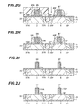
- the silicon nitride films 16 N, 16 P, 40 N and 40 P shown in FIG. 2H are etched and removed by phosphoric acid.
- the silicon oxide film 15 shown in FIG. 2I is anisotropically etched. Sidewall spacers 15 N of silicon oxide are left on the sidewalls of the gate electrode 6 N, and sidewall spacers 15 P are left on the sidewalls of the gate electrode 6 P.
- the area where the n-type well 4 is formed is covered with a resist pattern 45 .
- As ions are implanted to form extension regions 8 N and B ions are implanted to form pocket regions 9 N.
- These ion implantation conditions are the same as those for forming the extension regions 8 N and pocket regions 9 N of the first embodiment described with the process shown in FIG. 1B .
- the resist pattern 45 is removed.
- the area where the p-type well 3 is formed is covered with a resist pattern 46 .
- B ions are implanted to form extension regions 8 P and P ions are implanted to form pocket regions 9 P.
- These ion implantation conditions are the same as those for forming the extension regions 8 P and pocket regions 9 P of the first embodiment described with the process shown in FIG. 1C .
- the resist pattern 46 is removed.
- a heat treatment is performed for a very short time at 1050° C. to activate impurity ions implanted into the extension regions 8 N and 8 P and pocket regions 9 N and 9 P.
- This heat treatment time is sufficiently shorter than the heat treatment time (3 seconds) for activating the impurities implanted into the source and drain regions 31 N and 31 P. It is therefore possible to prevent the diffusion of impurities implanted into the extension regions 8 N and 8 P.
- the position at which the concentration distribution of impurities in the extension regions 8 N and 8 P in the depth direction takes a maximum value is shallower than that at which the concentration distribution of impurities in the source and drain regions 31 N and 31 P takes a maximum value.
- sidewall spacers 47 N of silicon nitride are formed on the outer sidewalls of the sidewall spacers 15 N, at the same time when sidewall spacers 47 P of silicon nitride are formed on the outer sidewalls of the sidewall spacers 15 P.
- These sidewall spacers 47 N and 47 P can be formed by depositing a silicon nitride film having a thickness of 80 nm and thereafter anisotropically etching it.
- the sidewall spacers 47 N reach at least the boundaries of the source and drain regions 31 N on the gate electrode 6 N side.
- the sidewall spacers 47 P reach at least the boundaries of the source and drain regions 31 P on the gate electrode 6 P side.
- CoSi 2 films 33 N, 33 P, 34 N and 34 P are formed on the upper surfaces of the source and drain regions 31 N, 31 P and gate electrodes 6 N and 6 P.
- the process of forming the CoSi 2 films 33 N, 33 P, 34 N and 34 P is the same as that of forming the CoSi 2 films 33 N, 33 P, 34 N and 34 P of the first embodiment shown in FIG. 1O .
- impurities are implanted only into the gate electrodes 6 N and 6 P without implanting impurities into the source and drain regions. It is therefore possible to set the impurity concentration of the gate electrodes 6 N and 6 P independently from that of the source and drain regions.
- ion implantation for forming the extension regions 8 N and 8 P is performed under the existence of the thin sidewall spacers 15 N and 15 P having a thickness in the order of 10 to 20 nm formed on the sidewalls of the gate electrodes 6 N and 6 P. It is therefore possible to prevent the ends of the extension regions 8 N and 8 P from entering farther under the gate electrodes 6 N and 6 P.
- the structure shown in FIG. 3A is the same as that of the first embodiment shown in FIG. 1A .
- the structure shown in FIG. 3A can be formed.
- an insulating film 50 having a thickness of, for example, 200 nm is formed by a spin-on-glass method, burying the gate electrodes 6 N and 6 P.
- the insulating film 50 is subjected to chemical mechanical polishing (CMP) until the upper surfaces of the gate electrodes 6 N and 6 P are exposed. It is not necessarily required to completely expose the upper surfaces of the gate electrodes 6 N and 6 P, but a thin film may be left on the gate electrodes to such an extent that the thin film will not function as a mask during ion implantation.
- CMP chemical mechanical polishing
- a film on the gate electrodes 6 N and 6 P can be thinned to a desired thickness by making the surface of the insulating film 50 by CMP or etch-back flatter than the surface of the insulating film immediately after it was formed.
- the surface area of the insulating film 50 above the n-type well 4 is covered with a resist pattern 51 . It is not necessarily required to cover the whole area above the n-type well 4 , but it is sufficient that at least the area above the gate electrode 6 P is covered with the insulating film 51 .
- P ions are implanted into the gate electrode 6 N.
- the P ion implantation conditions are the same as those for P ion implantation into the gate electrode 6 N of the first embodiment process described with reference to FIG. 1G . Since the substrate surface near the gate electrode 6 N is covered with the insulating film 50 , P ions are not implanted into the surface layer of the substrate 1 . After P ion implantation, the resist pattern 51 is removed.
- the surface area of the insulating film 50 above the p-type well 3 is covered with a resist pattern 52 . It is sufficient that at least the area above the gate electrode 6 N is covered with the insulating film 50 .
- B ions are implanted into the gate electrode 6 P.
- the B ion implantation conditions are the same as those for B ion implantation into the gate electrode 6 P of the first embodiment process described with reference to FIG. 1H . Since the substrate surface near the gate electrode 6 P is covered with the insulating film 50 , B ions are not implanted into the surface layer of the substrate 1 . After B ion implantation, the resist pattern 52 is removed.
- the insulating film 50 shown in FIG. 3E is removed by hydrofluoric acid.
- the insulating film 50 formed by SOG has an etching rate faster than the element separation insulating film 2 . It is therefore expected that the element separation insulating film 2 is hardly thinned while the insulating film 50 is etched.
- the area where the n-type well 4 is formed is covered with a resist pattern 53 .
- As ions are implanted to form extension regions 8 N and B ions are implanted to form pocket regions 9 N.
- the ion implantation conditions are the same as those for forming the extension regions 8 N and pocket regions 9 N of the first embodiment described with reference to FIG. 1B .
- the resist pattern 53 is removed.
- the area where the p-type well 3 is formed is covered with a resist pattern 54 .
- B ions are implanted to form extension regions 8 P and As ions are implanted to form pocket regions 9 P.
- the ion implantation conditions are the same as those for forming the extension regions 8 P and pocket regions 9 P of the first embodiment described with reference to FIG. 1C .
- the resist pattern 54 is removed.
- sidewall spacers 55 N and 55 P of silicon oxide or silicon nitride are formed on the sidewalls of the gate electrodes 6 N and 6 P.
- the sidewall spacers 55 N and 55 P are formed by a deposition process of a silicon oxide film or a silicon nitride film by CVD and an anisotropic etching process.
- the area where the n-type well 4 is formed is covered with a resist pattern 56 .
- a resist pattern 56 By using as a mask the gate electrode 6 N and sidewall spacers 55 N, P ions are implanted to form source and drain regions 31 N.
- the ion implantation conditions are the same as those for forming the source and drain regions 31 N described with the first embodiment process shown in FIG. 1L . After P ion implantation, the resist pattern 56 is removed.
- the area where the p-type well 3 is formed is covered with a resist pattern 57 .
- B ions are implanted to form source and drain regions 31 P.
- the ion implantation conditions are the same as those for forming the source and drain regions 31 P described with the first embodiment process shown in FIG. 1M .
- the resist pattern 57 shown in FIG. 3K is removed.
- a heat treatment is performed for about 3 seconds at a temperature of 1050° C. to activate implanted impurity ions.
- CoSi 2 films 33 N are formed on the surfaces of the source and drain regions 31 N and a CoSi 2 film 34 N is formed on the upper surface of the gate electrode 6 N, at the same time when CoSi 2 films 33 P are formed on the surfaces of the source and drain regions 31 P and a CoSi 2 film 34 P is formed on the upper surface of the gate electrode 6 P.
- impurities are implanted into the gate electrodes 6 N and 6 P by masking the surface layer of the substrate with the insulating film 50 . It is therefore possible to set the impurity concentration of the gate electrode independently from that of the source and drain regions.
- the surface of the substrate 1 in the process shown in FIG. 3B , although the surface of the substrate 1 is covered with the insulating film 50 formed by SOG, the surface of the substrate 1 may be covered with a resist film formed by spin-coating resist. After the surface of the substrate 1 is covered with the resist film, the surface of the resist film is planarized by CMP or etch-back to expose the upper surfaces of the gate electrodes 6 N and 6 P as shown in FIG. 3C .
- FIGS. 4A to 4H a semiconductor device manufacturing method according to a fourth embodiment of the invention will be described.
- the active region where a p-channel MOSFET is formed is shown, an n-channel MOSFET is formed in another active region not shown.
- a gate insulating film 5 P, a gate electrode 6 P, extension regions 8 P and pocket regions 9 P are formed on and in the surface layer of a silicon substrate 1 .
- the processes up to this structure are the same as the p-channel MOSFET forming processes of the first embodiment shown in FIGS. 1A to 1C .
- the height of the gate electrode 6 P is 110 nm and the gate length is 40 nm.
- the processes of forming an n-channel MOSFET are also the same as the n-channel MOSFET forming processes of the first embodiment shown in FIGS. 1A and 1B .
- a silicon nitride film is formed to a thickness of 40 to 100 nm by CVD, covering the whole surface of the substrate.
- the silicon nitride film is anisotropically etched to leave sidewall spacers 60 on the sidewalls of the gate electrode 6 P.
- boron (B) ions are implanted into the surface layer of the substrate 1 under the conditions of an acceleration energy of 1 to 2.5 keV and a dose of 2 ⁇ 10 15 cm ⁇ 2 .
- Source and drain regions 61 are therefore formed in the substrate surface layer outside of the sidewall spacers 60 , the source and drain regions being deeper than the extension regions 8 P.
- B ions are also implanted into the gate electrode 6 P, a region 62 implanted with B ions is only an upper partial region of the gate electrode 6 P and does not reach the bottom of the gate electrode.
- phosphorous (P) ions are implanted, for example, under the conditions of an acceleration energy of 3 to 6 keV and a dose of 5 ⁇ 10 15 cm ⁇ 2 .
- a silicon oxide film 65 is deposited on or over the whole surface of the substrate 1 to a thickness of 20 to 50 nm by CVD.
- the silicon oxide film 65 is anisotropically etched to leave second layer sidewall spacers 65 a on the first layer sidewall spacers 60 .
- B ions are implanted into the gate electrode 6 P under the conditions of an acceleration energy of 4 keV and a dose of 5 ⁇ 10 15 cm ⁇ 2 .
- B ions are also implanted into the substrate surface layer outside of the second layer sidewall spacers 65 a to form impurity diffusion regions 67 .
- P ions are implanted under the conditions of an acceleration energy of 10 keV and a dose of 8 ⁇ 10 15 cm ⁇ 2 .
- RTA rapid thermal annealing
- Impurities implanted into the gate electrode 6 P and substrate surface layer are therefore activated and diffused along the lateral and depth directions.
- the ends of the source and gate regions 61 on the gate electrode side enter the insides of the boundaries of the first layer sidewall spacers 60
- the ends of the impurity diffusion regions 67 on the gate electrode side enter the insides of the boundaries of the second layer sidewall spacers 65 a . Therefore, the first layer sidewall spacers 60 reach halfway the upper surfaces of the source and drain regions, namely cover the partial upper surfaces of the source and drain regions 61 .
- the second sidewall spacers 65 a shown in FIG. 4F are removed.
- the second layer sidewall spacers 65 a can be selectively removed by a wet process using hydrofluoric acid because the first layer sidewall spacers 60 are made of silicon nitride and the second layer sidewall spacers 65 a are made of silicon oxide.
- metal silicide films 68 of cobalt silicide or the like are formed on the gate electrode 6 P and on the surface of the active region not covered with the gate electrode 6 P and sidewall spacers 60 .
- the metal silicide films 68 can be formed, for example, by depositing a cobalt film on or over the substrate whole surface, performing a heat treatment to silicidize cobalt, and thereafter removing an unreacted cobalt film.
- the gate electrode is formed by patterning a polysilicon film not implanted with impurities, a variation of the cross section of the gate electrode 6 P can be suppressed.
- Impurities are not implanted to the bottom of the gate electrode 6 P during the ion implantation process for the source and drain regions 61 shown in FIG. 4B , but are implanted to the deep region of the gate electrode 6 P during the later process shown in FIG. 4E .
- Impurity ion implantation into the gate electrode 6 P shown in FIG. 4E and heat treatment shown in FIG. 4F are preferably performed under the condition that impurities implanted into the gate electrode 6 P reach the bottom of the gate electrodes 6 P after the heat treatment. By performing the impurity ion implantation and heat treatment under this condition, depletion of the gate electrode 6 P can be prevented.
- the source and drain regions 61 are shallow as compared to the height of the gate electrode 6 P.
- the acceleration energy for implanting impurity ions into the gate electrode 6 P shown in FIG. 4E is therefore generally higher than the acceleration energy of impurity ion implantation for forming the source and drain regions 61 shown in FIG. 4B .
- the sidewalls of the gate electrode 6 P While impurities are implanted into the gate electrode 6 P, the sidewalls of the gate electrode 6 P have two layers of the sidewall spacers 60 and 65 a which function as an ion implantation mask. Although the impurity diffusion regions 67 formed while impurities are implanted into the gate electrode are deeper than the source and drain regions 61 , the impurity diffusion regions are remote from the channel just under the gate electrode 6 P. The impurity diffusion regions 67 are therefore not likely to cause the punch-through phenomenon.
- the total thickness of two layers of the sidewall spacers 60 and 65 a necessary for preventing the punch-through phenomenon depends on the acceleration energy and dose when B ions are implanted into the gate electrode. If the acceleration energy is 4 keV and the dose is 1 ⁇ 10 15 cm ⁇ 2 , 4 ⁇ 10 15 cm ⁇ 2 , 8 ⁇ 10 15 cm ⁇ 2 or 1 ⁇ 10 16 cm ⁇ 2 , then it is preferable to set the total thickness of two layers of the sidewall spacers 60 and 65 a to 40 nm, 60 nm, 80 nm or 100 nm or thicker.
- the first layer sidewall spacers 60 shown in FIG. 4F are made of silicon nitride and the second layer sidewall spacers 65 a shown in FIG. 4F are made of silicon oxide. Since two layers of the sidewall spacers are made of insulating materials having different etching characteristics, only the second layer sidewall spacers 65 a can be selectively removed.
- the second layer sidewall spacers 65 a are made of silicon oxide, the second layer sidewall spacers 65 a can be removed by a pre-treatment of the silicidation process shown in FIG. 4H . Therefore, without increasing the number of processes, the second layer sidewall spacers 65 a can be removed.
- the upper surface of the gate electrode 6 P is exposed while impurities are implanted into the gate electrode 6 P shown in FIG. 4E . If a film of silicon oxide, silicon nitride or the like is formed on the gate electrode, atoms (nitrogen, oxygen) in the film are diffused into the gate electrode in some cases by the knock-on phenomenon. In the fourth embodiment, it is possible to prevent unexpected impurities from being diffused into the gate electrode.
- the sidewall spacers 60 formed on the extension regions 8 P shown in FIG. 4A are left unetched. If the sidewall spacers 60 are to be removed, the surface layer of the extension region 8 P is etched very slightly while the sidewall spacers 60 are removed. In such a case, this etch amount is required to be considered when the depth of the junction of the extension region 8 P is controlled. In the fourth embodiment, since there is no process of etching the sidewall spacers 60 , the depth of the extension region 8 P can be controlled only by the impurity ion implantation conditions.
- the silicon oxide film 65 which is formed by the process shown in FIG. 4C after the source and drain regions 61 are formed by the process shown in FIG. 4B , may be thinner than the first layer sidewall spacers 60 .
- a thermal load applied to the source and drain regions 61 can therefore be mitigated and impurity re-diffusion can be suppressed. Since the re-diffusion of the source and drain regions 61 can be suppressed, it is possible to prevent the short channel effects
Abstract
Description
Claims (5)
Priority Applications (1)
| Application Number | Priority Date | Filing Date | Title |
|---|---|---|---|
| US11/898,830 US8088666B2 (en) | 2001-11-26 | 2007-09-17 | Semiconductor device manufacture method including process of implanting impurity into gate electrode independently from source/drain and semiconductor device manufactured by the method |
Applications Claiming Priority (6)
| Application Number | Priority Date | Filing Date | Title |
|---|---|---|---|
| JP2001358754 | 2001-11-26 | ||
| JP2001-358754 | 2001-11-26 | ||
| JP2002314613A JP3980461B2 (en) | 2001-11-26 | 2002-10-29 | Manufacturing method of semiconductor device |
| JP2002-314613 | 2002-10-29 | ||
| US10/298,641 US7285449B2 (en) | 2001-11-26 | 2002-11-19 | Semiconductor device manufacture method including process of implanting impurity into gate electrode independently from source /drain and semiconductor device manufactured by the method |
| US11/898,830 US8088666B2 (en) | 2001-11-26 | 2007-09-17 | Semiconductor device manufacture method including process of implanting impurity into gate electrode independently from source/drain and semiconductor device manufactured by the method |
Related Parent Applications (1)
| Application Number | Title | Priority Date | Filing Date |
|---|---|---|---|
| US10/298,641 Division US7285449B2 (en) | 2001-11-26 | 2002-11-19 | Semiconductor device manufacture method including process of implanting impurity into gate electrode independently from source /drain and semiconductor device manufactured by the method |
Publications (2)
| Publication Number | Publication Date |
|---|---|
| US20080311721A1 US20080311721A1 (en) | 2008-12-18 |
| US8088666B2 true US8088666B2 (en) | 2012-01-03 |
Family
ID=26624679
Family Applications (2)
| Application Number | Title | Priority Date | Filing Date |
|---|---|---|---|
| US10/298,641 Expired - Lifetime US7285449B2 (en) | 2001-11-26 | 2002-11-19 | Semiconductor device manufacture method including process of implanting impurity into gate electrode independently from source /drain and semiconductor device manufactured by the method |
| US11/898,830 Expired - Fee Related US8088666B2 (en) | 2001-11-26 | 2007-09-17 | Semiconductor device manufacture method including process of implanting impurity into gate electrode independently from source/drain and semiconductor device manufactured by the method |
Family Applications Before (1)
| Application Number | Title | Priority Date | Filing Date |
|---|---|---|---|
| US10/298,641 Expired - Lifetime US7285449B2 (en) | 2001-11-26 | 2002-11-19 | Semiconductor device manufacture method including process of implanting impurity into gate electrode independently from source /drain and semiconductor device manufactured by the method |
Country Status (2)
| Country | Link |
|---|---|
| US (2) | US7285449B2 (en) |
| JP (1) | JP3980461B2 (en) |
Families Citing this family (11)
| Publication number | Priority date | Publication date | Assignee | Title |
|---|---|---|---|---|
| US20050026342A1 (en) * | 2003-07-28 | 2005-02-03 | Ka-Hing Fung | Semiconductor device having improved short channel effects, and method of forming thereof |
| WO2005057662A2 (en) * | 2003-12-10 | 2005-06-23 | Koninklijke Philips Electronics N.V. | Method and apparatus for fabricating ultra-shallow junction metal-oxide semiconductor integrated circuit devices. |
| JP4172796B2 (en) * | 2004-11-24 | 2008-10-29 | 株式会社東芝 | Manufacturing method of semiconductor device |
| JP2006173438A (en) * | 2004-12-17 | 2006-06-29 | Yamaha Corp | Method of manufacturing mos type semiconductor device |
| US7348248B2 (en) * | 2005-07-12 | 2008-03-25 | Taiwan Semiconductor Manufacturing Company, Ltd. | CMOS transistor with high drive current and low sheet resistance |
| JPWO2007080647A1 (en) * | 2006-01-13 | 2009-06-11 | 富士通マイクロエレクトロニクス株式会社 | Manufacturing method of semiconductor device |
| JP5034332B2 (en) * | 2006-06-14 | 2012-09-26 | 富士通セミコンダクター株式会社 | Manufacturing method of semiconductor device |
| JP2008071851A (en) * | 2006-09-13 | 2008-03-27 | Sony Corp | Semiconductor device and manufacturing method thereof |
| US20090104745A1 (en) * | 2007-10-23 | 2009-04-23 | Hyesook Hong | Integration method for dual doped polysilicon gate profile and cd control |
| DE102010063778B4 (en) * | 2010-12-21 | 2018-05-09 | Globalfoundries Dresden Module One Limited Liability Company & Co. Kg | Process for producing a gate electrode structure with increased structuring uniformity |
| US10964815B2 (en) * | 2018-06-12 | 2021-03-30 | Taiwan Semiconductor Manufacturing Company Ltd. | CMOS finFET with doped spacers and method for forming the same |
Citations (20)
| Publication number | Priority date | Publication date | Assignee | Title |
|---|---|---|---|---|
| US4735917A (en) | 1986-04-28 | 1988-04-05 | General Electric Company | Silicon-on-sapphire integrated circuits |
| JPH0423439A (en) | 1990-05-18 | 1992-01-27 | Fujitsu Ltd | Manufacture of semiconductor device |
| JPH05326552A (en) | 1992-03-19 | 1993-12-10 | Oki Electric Ind Co Ltd | Semiconductor element and its manufacture |
| JPH0794720A (en) | 1993-09-25 | 1995-04-07 | Ricoh Co Ltd | Semiconductor device |
| JPH07122737A (en) | 1993-10-22 | 1995-05-12 | Sanyo Electric Co Ltd | Semiconductor device and its manufacture |
| US5552346A (en) | 1995-04-27 | 1996-09-03 | Taiwan Semiconductor Manufacturing Co. | Planarization and etch back process for semiconductor layers |
| JPH09186317A (en) | 1995-12-28 | 1997-07-15 | Mitsubishi Electric Corp | Manufacture of semiconductor device |
| JPH09275149A (en) | 1996-04-04 | 1997-10-21 | Taiwan Moshii Denshi Kofun Yugenkoshi | Manufacture of complementary mos field effect transistor |
| JP2000150880A (en) | 1998-11-18 | 2000-05-30 | Toshiba Corp | Manufacture of semiconductor device |
| US6271125B1 (en) | 1999-02-18 | 2001-08-07 | Taiwan Semiconductor Manufacturing Company | Method to reduce contact hole aspect ratio for embedded DRAM arrays and logic devices, via the use of a tungsten bit line structure |
| US6294415B1 (en) * | 2000-04-26 | 2001-09-25 | United Microelectronics Corp. | Method of fabricating a MOS transistor |
| JP2001297996A (en) | 2000-04-13 | 2001-10-26 | Nec Corp | Manufacturing method of circuit and manufacturing device of circuit, annealing control method and annealing control device and information storage medium |
| US6340617B1 (en) * | 1998-11-30 | 2002-01-22 | Fujitsu Limited | Manufacture of semiconductor device |
| US20020008295A1 (en) * | 2000-07-22 | 2002-01-24 | Samsung Electronics Co., Ltd. | Metal oxide semiconductor field effect transistor for reducing resistance between source and drain and method for fabricating the same |
| US6413807B1 (en) * | 1999-06-29 | 2002-07-02 | Nec Corporation | Semiconductor device having silicide films on a gate electrode and a diffusion layer and manufacturing method thereof |
| US6462374B2 (en) * | 2000-06-30 | 2002-10-08 | Fujitsu Limited | Semiconductor device and method for fabricating the same |
| US6582995B2 (en) * | 2001-07-11 | 2003-06-24 | Taiwan Semiconductor Manufacturing Co., Ltd. | Method for fabricating a shallow ion implanted microelectronic structure |
| US6599819B1 (en) | 1999-05-26 | 2003-07-29 | Fujitsu Limited | Semiconductor device with source/drain regions of high impurity concentration and its manufacture |
| US6734070B1 (en) | 2003-03-17 | 2004-05-11 | Oki Electric Industry Co., Ltd. | Method of fabricating a semiconductor device with field-effect transistors having shallow source and drain junctions |
| US6808974B2 (en) * | 2001-05-15 | 2004-10-26 | International Business Machines Corporation | CMOS structure with maximized polysilicon gate activation and a method for selectively maximizing doping activation in gate, extension, and source/drain regions |
-
2002
- 2002-10-29 JP JP2002314613A patent/JP3980461B2/en not_active Expired - Fee Related
- 2002-11-19 US US10/298,641 patent/US7285449B2/en not_active Expired - Lifetime
-
2007
- 2007-09-17 US US11/898,830 patent/US8088666B2/en not_active Expired - Fee Related
Patent Citations (21)
| Publication number | Priority date | Publication date | Assignee | Title |
|---|---|---|---|---|
| US4735917A (en) | 1986-04-28 | 1988-04-05 | General Electric Company | Silicon-on-sapphire integrated circuits |
| JPH0423439A (en) | 1990-05-18 | 1992-01-27 | Fujitsu Ltd | Manufacture of semiconductor device |
| JPH05326552A (en) | 1992-03-19 | 1993-12-10 | Oki Electric Ind Co Ltd | Semiconductor element and its manufacture |
| JPH0794720A (en) | 1993-09-25 | 1995-04-07 | Ricoh Co Ltd | Semiconductor device |
| JPH07122737A (en) | 1993-10-22 | 1995-05-12 | Sanyo Electric Co Ltd | Semiconductor device and its manufacture |
| US5552346A (en) | 1995-04-27 | 1996-09-03 | Taiwan Semiconductor Manufacturing Co. | Planarization and etch back process for semiconductor layers |
| JPH09186317A (en) | 1995-12-28 | 1997-07-15 | Mitsubishi Electric Corp | Manufacture of semiconductor device |
| JPH09275149A (en) | 1996-04-04 | 1997-10-21 | Taiwan Moshii Denshi Kofun Yugenkoshi | Manufacture of complementary mos field effect transistor |
| JP2000150880A (en) | 1998-11-18 | 2000-05-30 | Toshiba Corp | Manufacture of semiconductor device |
| US6340617B1 (en) * | 1998-11-30 | 2002-01-22 | Fujitsu Limited | Manufacture of semiconductor device |
| US6271125B1 (en) | 1999-02-18 | 2001-08-07 | Taiwan Semiconductor Manufacturing Company | Method to reduce contact hole aspect ratio for embedded DRAM arrays and logic devices, via the use of a tungsten bit line structure |
| US6599819B1 (en) | 1999-05-26 | 2003-07-29 | Fujitsu Limited | Semiconductor device with source/drain regions of high impurity concentration and its manufacture |
| US6413807B1 (en) * | 1999-06-29 | 2002-07-02 | Nec Corporation | Semiconductor device having silicide films on a gate electrode and a diffusion layer and manufacturing method thereof |
| US6423602B2 (en) | 2000-04-13 | 2002-07-23 | Nec Corporation | Circuit manufacturing method and apparatus, anneal control method and apparatus, information storage medium |
| JP2001297996A (en) | 2000-04-13 | 2001-10-26 | Nec Corp | Manufacturing method of circuit and manufacturing device of circuit, annealing control method and annealing control device and information storage medium |
| US6294415B1 (en) * | 2000-04-26 | 2001-09-25 | United Microelectronics Corp. | Method of fabricating a MOS transistor |
| US6462374B2 (en) * | 2000-06-30 | 2002-10-08 | Fujitsu Limited | Semiconductor device and method for fabricating the same |
| US20020008295A1 (en) * | 2000-07-22 | 2002-01-24 | Samsung Electronics Co., Ltd. | Metal oxide semiconductor field effect transistor for reducing resistance between source and drain and method for fabricating the same |
| US6808974B2 (en) * | 2001-05-15 | 2004-10-26 | International Business Machines Corporation | CMOS structure with maximized polysilicon gate activation and a method for selectively maximizing doping activation in gate, extension, and source/drain regions |
| US6582995B2 (en) * | 2001-07-11 | 2003-06-24 | Taiwan Semiconductor Manufacturing Co., Ltd. | Method for fabricating a shallow ion implanted microelectronic structure |
| US6734070B1 (en) | 2003-03-17 | 2004-05-11 | Oki Electric Industry Co., Ltd. | Method of fabricating a semiconductor device with field-effect transistors having shallow source and drain junctions |
Non-Patent Citations (1)
| Title |
|---|
| Japanese Office Action dated Dec. 26, 2006, issued in corresponding Japanese Patent Application No. 2002-314613. |
Also Published As
| Publication number | Publication date |
|---|---|
| JP3980461B2 (en) | 2007-09-26 |
| US7285449B2 (en) | 2007-10-23 |
| JP2003224270A (en) | 2003-08-08 |
| US20030098486A1 (en) | 2003-05-29 |
| US20080311721A1 (en) | 2008-12-18 |
Similar Documents
| Publication | Publication Date | Title |
|---|---|---|
| US8088666B2 (en) | Semiconductor device manufacture method including process of implanting impurity into gate electrode independently from source/drain and semiconductor device manufactured by the method | |
| US5736419A (en) | Method of fabricating a raised source/drain MOSFET using self-aligned POCl3 for doping gate/source/drain regions | |
| US6309933B1 (en) | Method of fabricating T-shaped recessed polysilicon gate transistors | |
| US4753898A (en) | LDD CMOS process | |
| US7585739B2 (en) | Semiconductor device and method of fabricating the same | |
| US6917085B2 (en) | Semiconductor transistor using L-shaped spacer | |
| US6355955B1 (en) | Transistor and a method for forming the transistor with elevated and/or relatively shallow source/drain regions to achieve enhanced gate electrode formation | |
| US7154154B2 (en) | MOS transistors having inverted T-shaped gate electrodes | |
| US7009258B2 (en) | Method of building a CMOS structure on thin SOI with source/drain electrodes formed by in situ doped selective amorphous silicon | |
| US6709939B2 (en) | Method for fabricating semiconductor device | |
| JP2002026313A (en) | Semiconductor integrated circuit device and manufacturing method thereof | |
| JP2003188373A (en) | Semiconductor device and method of manufacturing the same | |
| US6943084B2 (en) | Semiconductor device on silicon-on-insulator and method for manufacturing the semiconductor device | |
| US20040219724A1 (en) | Methods of fabricating MOS field effect transistors with pocket regions | |
| US20020090787A1 (en) | Self-aligned elevated transistor | |
| US6562686B2 (en) | Method for fabricating semiconductor device | |
| US8004050B2 (en) | Semiconductor device comprising gate electrode having arsenic and phosphorous | |
| US20010053580A1 (en) | Inverted MOSFET process | |
| JP2002543609A (en) | Method of manufacturing shallow junction semiconductor device | |
| KR980012599A (en) | Methods of forming transistors using salicide process technology | |
| KR100613279B1 (en) | MOS transistor and fabrication method thereof | |
| JP2001203348A (en) | Semiconductor device and manufacturing method | |
| JPH10284589A (en) | Semiconductor device and its manufacture | |
| JPH07106569A (en) | Semiconductor device and its manufacture | |
| JPH06275823A (en) | Semiconductor device and its manufacture |
Legal Events
| Date | Code | Title | Description |
|---|---|---|---|
| AS | Assignment |
Owner name: FUJITSU MICROELECTRONICS LIMITED, JAPAN Free format text: ASSIGNMENT OF ASSIGNORS INTEREST;ASSIGNOR:FUJITSU LIMITED;REEL/FRAME:021976/0089 Effective date: 20081104 Owner name: FUJITSU MICROELECTRONICS LIMITED,JAPAN Free format text: ASSIGNMENT OF ASSIGNORS INTEREST;ASSIGNOR:FUJITSU LIMITED;REEL/FRAME:021976/0089 Effective date: 20081104 |
|
| AS | Assignment |
Owner name: FUJITSU SEMICONDUCTOR LIMITED, JAPAN Free format text: CHANGE OF NAME;ASSIGNOR:FUJITSU MICROELECTRONICS LIMITED;REEL/FRAME:024651/0744 Effective date: 20100401 |
|
| ZAAA | Notice of allowance and fees due |
Free format text: ORIGINAL CODE: NOA |
|
| ZAAB | Notice of allowance mailed |
Free format text: ORIGINAL CODE: MN/=. |
|
| FEPP | Fee payment procedure |
Free format text: PAYOR NUMBER ASSIGNED (ORIGINAL EVENT CODE: ASPN); ENTITY STATUS OF PATENT OWNER: LARGE ENTITY |
|
| STCF | Information on status: patent grant |
Free format text: PATENTED CASE |
|
| FPAY | Fee payment |
Year of fee payment: 4 |
|
| AS | Assignment |
Owner name: FUJITSU SEMICONDUCTOR LIMITED, JAPAN Free format text: CHANGE OF ADDRESS;ASSIGNOR:FUJITSU SEMICONDUCTOR LIMITED;REEL/FRAME:041188/0401 Effective date: 20160909 |
|
| MAFP | Maintenance fee payment |
Free format text: PAYMENT OF MAINTENANCE FEE, 8TH YEAR, LARGE ENTITY (ORIGINAL EVENT CODE: M1552); ENTITY STATUS OF PATENT OWNER: LARGE ENTITY Year of fee payment: 8 |
|
| FEPP | Fee payment procedure |
Free format text: MAINTENANCE FEE REMINDER MAILED (ORIGINAL EVENT CODE: REM.); ENTITY STATUS OF PATENT OWNER: LARGE ENTITY |
|
| LAPS | Lapse for failure to pay maintenance fees |
Free format text: PATENT EXPIRED FOR FAILURE TO PAY MAINTENANCE FEES (ORIGINAL EVENT CODE: EXP.); ENTITY STATUS OF PATENT OWNER: LARGE ENTITY |
|
| STCH | Information on status: patent discontinuation |
Free format text: PATENT EXPIRED DUE TO NONPAYMENT OF MAINTENANCE FEES UNDER 37 CFR 1.362 |
|
| FP | Lapsed due to failure to pay maintenance fee |
Effective date: 20240103 |