US8083324B2 - Inkjet printhead and method of manufacturing the same - Google Patents
Inkjet printhead and method of manufacturing the same Download PDFInfo
- Publication number
- US8083324B2 US8083324B2 US12/489,599 US48959909A US8083324B2 US 8083324 B2 US8083324 B2 US 8083324B2 US 48959909 A US48959909 A US 48959909A US 8083324 B2 US8083324 B2 US 8083324B2
- Authority
- US
- United States
- Prior art keywords
- layer
- material layer
- photosensitive resin
- substrate
- glue
- Prior art date
- Legal status (The legal status is an assumption and is not a legal conclusion. Google has not performed a legal analysis and makes no representation as to the accuracy of the status listed.)
- Expired - Fee Related, expires
Links
- 238000004519 manufacturing process Methods 0.000 title claims abstract description 16
- 239000011347 resin Substances 0.000 claims abstract description 140
- 229920005989 resin Polymers 0.000 claims abstract description 140
- 239000003292 glue Substances 0.000 claims abstract description 114
- 239000000758 substrate Substances 0.000 claims abstract description 56
- 238000000034 method Methods 0.000 claims abstract description 48
- 239000003112 inhibitor Substances 0.000 claims abstract description 38
- 230000008569 process Effects 0.000 claims abstract description 29
- 239000000463 material Substances 0.000 claims description 208
- 238000002161 passivation Methods 0.000 claims description 26
- 239000002904 solvent Substances 0.000 claims description 17
- 239000003513 alkali Substances 0.000 claims description 16
- 238000009792 diffusion process Methods 0.000 claims description 14
- 239000003795 chemical substances by application Substances 0.000 claims description 13
- 150000008366 benzophenones Chemical class 0.000 claims description 8
- 125000003354 benzotriazolyl group Chemical class N1N=NC2=C1C=CC=C2* 0.000 claims description 8
- 125000000332 coumarinyl group Chemical class O1C(=O)C(=CC2=CC=CC=C12)* 0.000 claims description 8
- WRAQQYDMVSCOTE-UHFFFAOYSA-N phenyl prop-2-enoate Chemical class C=CC(=O)OC1=CC=CC=C1 WRAQQYDMVSCOTE-UHFFFAOYSA-N 0.000 claims description 8
- YGSDEFSMJLZEOE-UHFFFAOYSA-N salicylic acid Chemical class OC(=O)C1=CC=CC=C1O YGSDEFSMJLZEOE-UHFFFAOYSA-N 0.000 claims description 8
- YRHRIQCWCFGUEQ-UHFFFAOYSA-N thioxanthen-9-one Chemical class C1=CC=C2C(=O)C3=CC=CC=C3SC2=C1 YRHRIQCWCFGUEQ-UHFFFAOYSA-N 0.000 claims description 8
- 238000002835 absorbance Methods 0.000 claims description 6
- 238000000059 patterning Methods 0.000 claims description 4
- 238000010438 heat treatment Methods 0.000 description 6
- 238000010030 laminating Methods 0.000 description 6
- XUIMIQQOPSSXEZ-UHFFFAOYSA-N Silicon Chemical compound [Si] XUIMIQQOPSSXEZ-UHFFFAOYSA-N 0.000 description 5
- 229910052710 silicon Inorganic materials 0.000 description 5
- 239000010703 silicon Substances 0.000 description 5
- 229910000838 Al alloy Inorganic materials 0.000 description 4
- NTIZESTWPVYFNL-UHFFFAOYSA-N Methyl isobutyl ketone Chemical compound CC(C)CC(C)=O NTIZESTWPVYFNL-UHFFFAOYSA-N 0.000 description 4
- UIHCLUNTQKBZGK-UHFFFAOYSA-N Methyl isobutyl ketone Natural products CCC(C)C(C)=O UIHCLUNTQKBZGK-UHFFFAOYSA-N 0.000 description 4
- VYPSYNLAJGMNEJ-UHFFFAOYSA-N Silicium dioxide Chemical compound O=[Si]=O VYPSYNLAJGMNEJ-UHFFFAOYSA-N 0.000 description 4
- 229910052782 aluminium Inorganic materials 0.000 description 4
- XAGFODPZIPBFFR-UHFFFAOYSA-N aluminium Chemical compound [Al] XAGFODPZIPBFFR-UHFFFAOYSA-N 0.000 description 4
- BGTOWKSIORTVQH-UHFFFAOYSA-N cyclopentanone Chemical compound O=C1CCCC1 BGTOWKSIORTVQH-UHFFFAOYSA-N 0.000 description 4
- 239000010931 gold Substances 0.000 description 4
- 230000001678 irradiating effect Effects 0.000 description 4
- LLHKCFNBLRBOGN-UHFFFAOYSA-N propylene glycol methyl ether acetate Chemical compound COCC(C)OC(C)=O LLHKCFNBLRBOGN-UHFFFAOYSA-N 0.000 description 4
- 229910052814 silicon oxide Inorganic materials 0.000 description 4
- 239000002585 base Substances 0.000 description 3
- 230000008901 benefit Effects 0.000 description 3
- 239000007772 electrode material Substances 0.000 description 3
- 239000012776 electronic material Substances 0.000 description 3
- 239000012535 impurity Substances 0.000 description 3
- 230000000149 penetrating effect Effects 0.000 description 3
- YEJRWHAVMIAJKC-UHFFFAOYSA-N 4-Butyrolactone Chemical compound O=C1CCCO1 YEJRWHAVMIAJKC-UHFFFAOYSA-N 0.000 description 2
- RYGMFSIKBFXOCR-UHFFFAOYSA-N Copper Chemical compound [Cu] RYGMFSIKBFXOCR-UHFFFAOYSA-N 0.000 description 2
- 101000851376 Homo sapiens Tumor necrosis factor receptor superfamily member 8 Proteins 0.000 description 2
- 229910052581 Si3N4 Inorganic materials 0.000 description 2
- BQCADISMDOOEFD-UHFFFAOYSA-N Silver Chemical compound [Ag] BQCADISMDOOEFD-UHFFFAOYSA-N 0.000 description 2
- NRTOMJZYCJJWKI-UHFFFAOYSA-N Titanium nitride Chemical compound [Ti]#N NRTOMJZYCJJWKI-UHFFFAOYSA-N 0.000 description 2
- 102100036857 Tumor necrosis factor receptor superfamily member 8 Human genes 0.000 description 2
- RVSGESPTHDDNTH-UHFFFAOYSA-N alumane;tantalum Chemical compound [AlH3].[Ta] RVSGESPTHDDNTH-UHFFFAOYSA-N 0.000 description 2
- 230000015572 biosynthetic process Effects 0.000 description 2
- 229910052802 copper Inorganic materials 0.000 description 2
- 239000010949 copper Substances 0.000 description 2
- 238000000151 deposition Methods 0.000 description 2
- PCHJSUWPFVWCPO-UHFFFAOYSA-N gold Chemical compound [Au] PCHJSUWPFVWCPO-UHFFFAOYSA-N 0.000 description 2
- 229910052737 gold Inorganic materials 0.000 description 2
- 229910052751 metal Inorganic materials 0.000 description 2
- 239000002184 metal Substances 0.000 description 2
- 230000001590 oxidative effect Effects 0.000 description 2
- HQVNEWCFYHHQES-UHFFFAOYSA-N silicon nitride Chemical compound N12[Si]34N5[Si]62N3[Si]51N64 HQVNEWCFYHHQES-UHFFFAOYSA-N 0.000 description 2
- 229910052709 silver Inorganic materials 0.000 description 2
- 239000004332 silver Substances 0.000 description 2
- 229910052715 tantalum Inorganic materials 0.000 description 2
- GUVRBAGPIYLISA-UHFFFAOYSA-N tantalum atom Chemical compound [Ta] GUVRBAGPIYLISA-UHFFFAOYSA-N 0.000 description 2
- MZLGASXMSKOWSE-UHFFFAOYSA-N tantalum nitride Chemical compound [Ta]#N MZLGASXMSKOWSE-UHFFFAOYSA-N 0.000 description 2
- WQJQOUPTWCFRMM-UHFFFAOYSA-N tungsten disilicide Chemical compound [Si]#[W]#[Si] WQJQOUPTWCFRMM-UHFFFAOYSA-N 0.000 description 2
- 229910021342 tungsten silicide Inorganic materials 0.000 description 2
- 238000001039 wet etching Methods 0.000 description 2
- 239000000853 adhesive Substances 0.000 description 1
- 230000001070 adhesive effect Effects 0.000 description 1
- 230000002411 adverse Effects 0.000 description 1
- 239000011248 coating agent Substances 0.000 description 1
- 238000000576 coating method Methods 0.000 description 1
- 239000004020 conductor Substances 0.000 description 1
- 238000007599 discharging Methods 0.000 description 1
- 238000001312 dry etching Methods 0.000 description 1
- 238000005530 etching Methods 0.000 description 1
- -1 for example Substances 0.000 description 1
- 230000006872 improvement Effects 0.000 description 1
- 239000011810 insulating material Substances 0.000 description 1
- 230000007246 mechanism Effects 0.000 description 1
- 230000009466 transformation Effects 0.000 description 1
Images


Classifications
-
- B—PERFORMING OPERATIONS; TRANSPORTING
- B41—PRINTING; LINING MACHINES; TYPEWRITERS; STAMPS
- B41J—TYPEWRITERS; SELECTIVE PRINTING MECHANISMS, i.e. MECHANISMS PRINTING OTHERWISE THAN FROM A FORME; CORRECTION OF TYPOGRAPHICAL ERRORS
- B41J2/00—Typewriters or selective printing mechanisms characterised by the printing or marking process for which they are designed
- B41J2/005—Typewriters or selective printing mechanisms characterised by the printing or marking process for which they are designed characterised by bringing liquid or particles selectively into contact with a printing material
- B41J2/01—Ink jet
- B41J2/135—Nozzles
- B41J2/16—Production of nozzles
- B41J2/1601—Production of bubble jet print heads
- B41J2/1603—Production of bubble jet print heads of the front shooter type
-
- B—PERFORMING OPERATIONS; TRANSPORTING
- B41—PRINTING; LINING MACHINES; TYPEWRITERS; STAMPS
- B41J—TYPEWRITERS; SELECTIVE PRINTING MECHANISMS, i.e. MECHANISMS PRINTING OTHERWISE THAN FROM A FORME; CORRECTION OF TYPOGRAPHICAL ERRORS
- B41J2/00—Typewriters or selective printing mechanisms characterised by the printing or marking process for which they are designed
- B41J2/005—Typewriters or selective printing mechanisms characterised by the printing or marking process for which they are designed characterised by bringing liquid or particles selectively into contact with a printing material
- B41J2/01—Ink jet
- B41J2/135—Nozzles
- B41J2/14—Structure thereof only for on-demand ink jet heads
- B41J2/14016—Structure of bubble jet print heads
- B41J2/14032—Structure of the pressure chamber
- B41J2/1404—Geometrical characteristics
-
- B—PERFORMING OPERATIONS; TRANSPORTING
- B41—PRINTING; LINING MACHINES; TYPEWRITERS; STAMPS
- B41J—TYPEWRITERS; SELECTIVE PRINTING MECHANISMS, i.e. MECHANISMS PRINTING OTHERWISE THAN FROM A FORME; CORRECTION OF TYPOGRAPHICAL ERRORS
- B41J2/00—Typewriters or selective printing mechanisms characterised by the printing or marking process for which they are designed
- B41J2/005—Typewriters or selective printing mechanisms characterised by the printing or marking process for which they are designed characterised by bringing liquid or particles selectively into contact with a printing material
- B41J2/01—Ink jet
- B41J2/135—Nozzles
- B41J2/14—Structure thereof only for on-demand ink jet heads
- B41J2/14016—Structure of bubble jet print heads
- B41J2/14088—Structure of heating means
- B41J2/14112—Resistive element
- B41J2/14129—Layer structure
-
- B—PERFORMING OPERATIONS; TRANSPORTING
- B41—PRINTING; LINING MACHINES; TYPEWRITERS; STAMPS
- B41J—TYPEWRITERS; SELECTIVE PRINTING MECHANISMS, i.e. MECHANISMS PRINTING OTHERWISE THAN FROM A FORME; CORRECTION OF TYPOGRAPHICAL ERRORS
- B41J2/00—Typewriters or selective printing mechanisms characterised by the printing or marking process for which they are designed
- B41J2/005—Typewriters or selective printing mechanisms characterised by the printing or marking process for which they are designed characterised by bringing liquid or particles selectively into contact with a printing material
- B41J2/01—Ink jet
- B41J2/135—Nozzles
- B41J2/16—Production of nozzles
- B41J2/1621—Manufacturing processes
- B41J2/1623—Manufacturing processes bonding and adhesion
-
- B—PERFORMING OPERATIONS; TRANSPORTING
- B41—PRINTING; LINING MACHINES; TYPEWRITERS; STAMPS
- B41J—TYPEWRITERS; SELECTIVE PRINTING MECHANISMS, i.e. MECHANISMS PRINTING OTHERWISE THAN FROM A FORME; CORRECTION OF TYPOGRAPHICAL ERRORS
- B41J2/00—Typewriters or selective printing mechanisms characterised by the printing or marking process for which they are designed
- B41J2/005—Typewriters or selective printing mechanisms characterised by the printing or marking process for which they are designed characterised by bringing liquid or particles selectively into contact with a printing material
- B41J2/01—Ink jet
- B41J2/135—Nozzles
- B41J2/16—Production of nozzles
- B41J2/1621—Manufacturing processes
- B41J2/1626—Manufacturing processes etching
- B41J2/1629—Manufacturing processes etching wet etching
-
- B—PERFORMING OPERATIONS; TRANSPORTING
- B41—PRINTING; LINING MACHINES; TYPEWRITERS; STAMPS
- B41J—TYPEWRITERS; SELECTIVE PRINTING MECHANISMS, i.e. MECHANISMS PRINTING OTHERWISE THAN FROM A FORME; CORRECTION OF TYPOGRAPHICAL ERRORS
- B41J2/00—Typewriters or selective printing mechanisms characterised by the printing or marking process for which they are designed
- B41J2/005—Typewriters or selective printing mechanisms characterised by the printing or marking process for which they are designed characterised by bringing liquid or particles selectively into contact with a printing material
- B41J2/01—Ink jet
- B41J2/135—Nozzles
- B41J2/16—Production of nozzles
- B41J2/1621—Manufacturing processes
- B41J2/1631—Manufacturing processes photolithography
-
- Y—GENERAL TAGGING OF NEW TECHNOLOGICAL DEVELOPMENTS; GENERAL TAGGING OF CROSS-SECTIONAL TECHNOLOGIES SPANNING OVER SEVERAL SECTIONS OF THE IPC; TECHNICAL SUBJECTS COVERED BY FORMER USPC CROSS-REFERENCE ART COLLECTIONS [XRACs] AND DIGESTS
- Y10—TECHNICAL SUBJECTS COVERED BY FORMER USPC
- Y10T—TECHNICAL SUBJECTS COVERED BY FORMER US CLASSIFICATION
- Y10T29/00—Metal working
- Y10T29/49—Method of mechanical manufacture
- Y10T29/49401—Fluid pattern dispersing device making, e.g., ink jet
Definitions
- the present disclosure relates generally to a thermal inkjet printhead and a method of manufacturing the thermal inkjet printhead.
- An inkjet printhead is a device that discharges small droplets of ink at desired locations on a printing medium through nozzles, thereby forming a visible image of one or more color.
- an inkjet printhead may be classified into one of two types according to the mechanism employed for discharging the ink droplets.
- the first type is a thermal inkjet printhead that generates bubbles in ink using a heat source, and that discharges the ink droplets by the expansive force of the bubbles.
- the second type is a piezoelectric inkjet printhead, which uses a piezoelectric material to discharge the ink droplets by a pressure applied to ink due to transformation of the piezoelectric material.
- the thermal type inkjet printhead when a pulse type current flows through a heater formed, e.g., of a resistive heating element, the heat generated in the heater heats the ink adjacent to the heater almost instantly to about 300° C. As a result, the ink starts to boil, resulting the formation of ink bubbles that expand to apply a pressure to the ink filled in an ink chamber. The pressure causes the ink adjacent a nozzle to discharge from the ink chamber through the nozzle in the form of droplets. In a thermal inkjet printhead, it is generally understood that the nozzles have to be uniformly formed in order to achieve print quality.
- an inkjet printhead may include: a substrate having an ink feed hole; a chamber layer formed above the substrate, the chamber layer defining a plurality of ink chambers; a nozzle layer formed above the chamber layer, the nozzle layer having formed therein a plurality of nozzles; and a glue layer interposed between the substrate and the chamber layer, the glue layer containing a crosslink inhibitor.
- the glue layer may comprise a first negative type photosensitive resin soluble in a first type developing agent.
- the chamber layer may comprise a second negative type photosensitive resin that is not soluble in the first type developing agent.
- the first negative type photosensitive resin may be a solvent soluble resin while the second negative type photosensitive resin may be an alkali soluble resin.
- the first negative type photosensitive resin may be an alkali soluble resin while the second negative type photosensitive resin may be a solvent soluble resin.
- the crosslink inhibitor may inhibit cross linkage of the first negative type photosensitive resin during an exposing process.
- the crosslink inhibitor may comprise a light absorbing dye.
- the glue layer may comprise a photosensitive resin and photoacid generator (PGA) that promotes cross linkage of the photosensitive resin.
- the light absorbing dye may absorb light having the same wavelength as the light absorbance wavelength of the PGA to thereby inhibit cross linkage of the photosensitive resin.
- the light absorbing dye may comprise at least one material selected from the group consisting of benzophenone compounds, salicylic acid compounds, phenylacrylate compounds, benzotriazole compounds, coumarin compounds and thioxanthone compounds.
- the amount of the light absorbing dye may be about 0.03-5 parts by weight based on 100 parts by weight of the photosensitive resin included in the glue layer.
- the inkjet printhead may further comprise an insulating layer formed on the substrate; a plurality of heaters and electrodes sequentially formed on the insulating layer; and a passivation layer covering the heaters and the electrodes.
- a method of manufacturing an inkjet printhead may include forming an ink feed hole in a substrate; providing a glue material layer containing a crosslink inhibitor above the substrate, and exposing the glue material layer; forming one or more ink chambers by providing a chamber material layer above the glue material layer, and by exposing and developing the chamber material layer; providing a nozzle material layer on the chamber layer, and exposing the nozzle material layer; and developing the nozzle material layer and the glue material layer.
- the chamber material layer may be developed using a first type developing agent.
- the glue material layer may not be soluble in the first type developing agent.
- the crosslink inhibitor may inhibit cross linkage of the photosensitive resin included in the glue material layer during the exposing process.
- the crosslink inhibitor may comprises a light absorbing dye.
- the glue layer may comprise a photosensitive resin and photoacid generator (PGA) that promotes cross linkage of the photosensitive resin.
- the light absorbing dye may absorb light having the same wavelength as the light absorbance wavelength of the PGA to thereby inhibit cross linkage of the photosensitive resin.
- the light absorbing dye may comprise at least one material selected from the group consisting of benzophenone compounds, salicylic acid compounds, phenylacrylate compounds, benzotriazole compounds, coumarin compounds and thioxanthone compounds.
- the amount of the light absorbing dye may be about 0.03-5 parts by weight based on 100 parts by weight of the photosensitive resin included in the glue material layer.
- At least one of the glue material layer, the chamber material layer and the nozzle material layer may be formed of a photosensitive dry film.
- the method may further include forming an insulating layer on the substrate; sequentially forming a plurality of heaters and electrodes on the insulating layer; and forming a passivation layer covering the heaters and the electrodes.
- the step of forming the ink feed hole may be performed prior to the step of providing the glue material layer.
- the step of forming the ink feed hole may comprises removing a portion of the substrate staring from the top surface of the substrate continuing to the bottom surface of the substrate so as to create a hole that penetrates through the substrate.
- the step of forming the ink feed hole may be performed after to the step of developing the nozzle material layer and the glue material layer.
- the step of forming the ink feed hole may comprise removing a portion of the substrate staring from the bottom surface of the substrate continuing to the top surface of the substrate so as to create a hole that penetrates through the substrate.
- a method of fabricating an inkjet printhead may include forming an anti-diffusion reflection layer above a substrate, the anti-diffusion reflection layer having substantially planar surface, and containing a quantity of crosslink inhibitor; and exposing a nozzle material layer provided above the anti-diffusion reflection layer with light to form a pattern of nozzles on the nozzle material layer.
- the method may further include forming one or more ink chambers between the nozzle material layer and the anti-diffusion reflection layer by patterning a chamber material layer placed between the nozzle material layer and the anti-diffusion reflection layer.
- the chamber material layer may be developed using a first type developing agent.
- the anti-diffusion reflection layer may not be soluble in the first type developing agent.
- the anti-diffusion reflection layer may comprise a first negative type photosensitive resin.
- the chamber material layer may comprise a second negative type photosensitive resin.
- the first negative type photosensitive resin may be one of a solvent soluble resin and an alkali soluble resin while the second negative type photosensitive resin may be the other one of the solvent soluble resin and the alkali soluble resin.
- the crosslink inhibitor may be a light absorbing dye that may comprises at least one material selected from the group consisting of benzophenone compounds, salicylic acid compounds, phenylacrylate compounds, benzotriazole compounds, coumarin compounds and thioxanthone compounds.
- FIG. 1 is a plan view schematically illustrating an inkjet printhead according to an embodiment of the present disclosure
- FIG. 2 is a cross-sectional view taken along the line II-II′ of FIG. 1 ;
- FIGS. 3 through 10 are cross-sectional views for illustrating a method of manufacturing an inkjet printhead according to an embodiment of the present disclosure
- FIG. 11 illustrates a nozzle material layer that is exposed when a glue material layer including a crosslink inhibitor is not formed on a passivation layer
- FIGS. 12 through 18 are cross-sectional views for illustrating a method of manufacturing an inkjet printhead according to another embodiment of the present disclosure.
- FIG. 1 is a plan view schematically illustrating an inkjet printhead according to an embodiment.
- FIG. 2 is a cross-sectional view taken along the line II-II′ of FIG. 1 .
- a glue layer 121 , a chamber layer 120 , and a nozzle layer 130 may be formed on a substrate 110 on which a plurality of material layers are formed
- the substrate 110 may be formed of, for example, silicon, but the material for the substrate is not so limited, and materials other than silicon could also be used.
- the substrate 110 may include an ink feed hole 111 penetrating therethrough.
- a plurality of ink chambers 122 may be formed in the chamber layer 120 .
- a plurality of nozzles 132 may be formed in the nozzle layer 130 .
- An insulating layer 112 may be provided between the substrate 110 and heaters 114 , which will be described in greater detail later.
- the insulating layer 112 may be formed of an insulating material, for example, a silicon oxide, or the like.
- a plurality of heaters 112 for heating the ink in the ink chambers 122 to generate the ink bubbles may be formed on the insulating layer 112 .
- the heaters 114 may be formed of a heating resistor, for example, a tantalum-aluminum alloy, a tantalum nitride, a titanium nitride, tungsten silicide, or the like.
- the material for forming the heaters is not limited to those above specific examples.
- a plurality of electrodes 116 may be formed on the upper surface of the heaters 114 .
- the electrodes 116 are used to apply the current to the heaters 114 , and may be formed of any electrically conductive material, including, for example, aluminum (Al), an aluminum alloy, gold (Au), silver (Ag), or the like.
- a passivation layer 118 may be formed on the upper surfaces of the heaters 114 and the electrodes 116 . The passivation layer 118 prevents the heaters 114 and the electrodes 116 from oxidizing or corroding due to contact with ink, and may be formed of, for example, a silicon nitride, a silicon oxide, or the like.
- An anti-cavitation layer 119 may be formed on the upper surface of the passivation layer 118 , which is disposed on the heaters 1 14 .
- the anti-cavitation layer 119 protects the heaters 114 from a cavitation force generated when the bubbles burst, and may be formed of, for example, tantalum (Ta), or the like.
- a glue layer 121 is formed on the passivation layer 118 in order to increase an adhesive strength between the chamber layer 120 and the substrate 110 .
- the thickness of the glue layer 121 may be about 0.5-10 ⁇ m, and, preferably, 2-5 ⁇ m, for example. However, it should be noted that the above glue layer thicknesses are merely examples, and should not be construed to limiting the thickness to those specific examples.
- the glue layer 121 may include a photosensitive resin, for example, a negative type photosensitive resin. The photosensitive resin included in the glue layer 121 and the photosensitive resin included in the chamber layer 120 , which will be described in greater detail later, may be developed using different developing solutions.
- the photosensitive resin included in the glue layer 121 may be a solvent soluble resin while the photosensitive resin included in the chamber layer 120 may be an alkali soluble resin.
- the photosensitive resin included in the glue layer 121 may be an alkali soluble resin while the photosensitive resin included in the chamber layer 120 may be a solvent soluble resin. This will be described in more detail later with reference to the embodiments of the methods of manufacturing the inkjet printhead.
- the glue layer 121 may further include a crosslink inhibitor.
- the crosslink inhibitor may inhibit cross linkage of the photosensitive resin included in the glue layer 121 during an exposing process. More specifically, the crosslink inhibitor may inhibit cross linkage of the photosensitive resin included in a glue material layer 121 ′ (shown in FIG. 9 ) during the exposure of the nozzle material layer 130 ′ (see FIG. 9 ). That is, when exposing the nozzle material layer 130 ′, cross linkage of the photosensitive resin may take place in portions of the exposed nozzle material layer 130 ′, but substantially no cross linkage of the photosensitive resin occurs in the glue material layer 121 ′. This will be described in more detail later with reference to embodiments of the methods of manufacturing the inkjet printhead.
- the crosslink inhibitor may be, for example, a light absorbing dye.
- the light absorbing dye absorbs light having the same wavelength as the light absorbance wavelength of a photoacid generator (PGA), which generates the cross linkage of the photosensitive resin during the exposing process, and thus may inhibit cross linkage of the photosensitive resin.
- PGA photoacid generator
- Examples of the light absorbing dye may include at least one material selected from the group consisting of benzophenone compounds, salicylic acid compounds, phenylacrylate compounds, benzotriazole compounds, coumarin compounds, and thioxanthone compounds.
- the material for forming the light absorbing dye is not limited to the above specific examples.
- An amount of the light absorbing dye included in the glue layer 121 may be about 0.03-5 parts by weight based on 100 parts by weight of the photosensitive resin included in the glue layer 121 .
- the light absorbing dye described above is only an example of the crosslink inhibitor, and the same should not be construed as a limitation.
- the chamber layer 120 is formed on the glue layer 121 .
- the ink chambers 122 in which ink supplied through the ink feed hole 111 may be filled, are formed on the chamber layer 120 .
- a plurality of restrictors 124 which act as the paths from the ink feed hole 111 to the ink chambers 122 , may further be formed in the chamber layer 120 .
- the chamber layer 120 may include a negative type photosensitive resin. As described above, the photosensitive resin included in the glue layer 121 and the photosensitive resin included in the chamber layer 120 may be developed using different developing solutions.
- the nozzle layer 130 is formed above the chamber layer 120 .
- the nozzles 132 through which ink is discharged may be formed on the nozzle layer 130 .
- the nozzle layer 130 may include a negative type photosensitive resin.
- the glue layer 121 including the crosslink inhibitor may be formed between the substrate 110 and the chamber layer 120 so that a diffused reflection, which may be caused by exposing the nozzle material layer 130 ′ (shown in FIG. 9 ), may be prevented, and thereby, the nozzles 132 may be uniformly formed as desired.
- the substrate 110 is prepared and the insulating layer 112 may be formed on the upper surface of the substrate 110 .
- the substrate 110 may, e.g., be a silicon substrate.
- the insulating layer 112 insulates the substrate 110 and the heaters from each other, and may be formed of, for example, silicon oxide.
- the heaters 114 for heating the ink and for generating the ink bubbles may be formed on the upper surface of the insulating layer 112 .
- the heaters 114 may be formed by depositing a layer of heating resistor composed of; for example, a tantalum-aluminum alloy, a tantalum nitride, a titanium nitride, tungsten silicide, or the like, on the upper surface of the insulating layer 112 , and by patterning the deposited heating resistor layer. Then, the electrodes 116 for applying the current to the heaters 114 may be formed on the upper surface of the heaters 114 .
- a layer of heating resistor composed of; for example, a tantalum-aluminum alloy, a tantalum nitride, a titanium nitride, tungsten silicide, or the like.
- the electrodes 116 may be formed, e.g., by depositing a layer metal having sufficient electrical conductivity, for example, aluminum (Al), an aluminum alloy, gold (Au), silver (Ag), or the like, on the upper surfaces of the heaters 114 , and then by patterning the deposited metal layer.
- a layer metal having sufficient electrical conductivity for example, aluminum (Al), an aluminum alloy, gold (Au), silver (Ag), or the like.
- the passivation layer 118 may be formed on the insulating layer 112 to cover the heaters 114 and the electrodes 116 .
- the passivation layer 118 prevents the heaters 114 and the electrodes 116 from oxidizing or corroding due to contact with ink, and may be formed of, for example, a silicon nitride, a silicon oxide, or the like.
- the anti-cavitation layer 119 may additionally be formed on the upper surface of the passivation layer 118 , which is disposed on the heaters 114 .
- the anti-cavitation layer 119 protects the heaters 114 from a cavitation force generated bubbles burst, and may be formed of, for example, tantalum (Ta), or the like.
- the ink feed hole 111 may be formed in the substrate 110 by, e.g., sequentially processing the passivation layer 118 , the insulating layer 112 , and the substrate 110 .
- the ink feed hole 111 may be formed by using, for example, dry etching, wet etching, or laser processing.
- the ink feed hole 111 may be formed to penetrate the substrate 110 from the upper surface thereof to the lower surface thereof.
- An advantage of processing from the upper portion of the substrate 110 to form the ink feed hole 111 may be that the properly forming the upper portion of the ink feed hole 111 at the desired location may become relatively easier.
- the ink feed hole 111 may be formed by processing from the bottom of the substrate 110 .
- a glue material layer 121 ′ may be formed above the passivation layer 118 as shown in FIG. 5 .
- the thickness of the glue material layer 121 ′ may be about 0.5-10 ⁇ m, or more preferably 2-5 ⁇ m, for example.
- the thickness of the glue material layer 121 ′ however is not limited to the above specific examples.
- the glue material layer 121 ′ may include a negative type photosensitive resin, a photoacid generator (PAG) and a crosslink inhibitor.
- the glue material layer 121 ′ may be formed by laminating a photosensitive dry film including the negative type photosensitive resin, the PAG and the crosslink inhibitor on the passivation layer 118 .
- the PAG absorbs light having a predetermined wavelength during the exposing of the glue material layer 121 ′, and generates H + , thereby generating cross linkage of the photosensitive resin.
- the crosslink inhibitor inhibits cross linkage of the photosensitive resin included in the glue material layer 121 ′ up to certain amount of light exposure during the exposing of the glue material layer 121 ′, but when the amount of light exposure exceeds the threshold amount, the crosslink inhibitor loses its effectiveness, and thus allows the cross linkage of the photosensitive resin by the PAG to occur.
- the crosslink inhibitor may be, for example, a light absorbing dye.
- the light absorbing dye absorbs light having the same wavelength as the light absorbance wavelength of the PAG, and thus inhibits PAG from absorbing light. Accordingly, cross linkage of the photosensitive resin may be inhibited in parts of the exposed glue material layer 121 ′.
- the light absorbing dye may include at least one material selected from the group consisting of benzophenone compounds, salicylic acid compounds, phenylacrylate compounds, benzotriazole compounds, coumarin compounds, and thioxanthone compounds.
- the material for forming the light absorbing dye is not limited to those above.
- the amount of the light absorbing dye included in the glue material layer 121 ′ may be about 0.03-5 parts by weight based on 100 parts by weight of the photosensitive resin included in the glue material layer 121 ′.
- the glue material layer 121 ′ may be formed of 100 parts by weight of the negative type photosensitive resin, 4 parts by weight of the PAG, and 2 parts by weight of the light absorbing dye.
- a predetermined base material may be used as the crosslink inhibitor.
- a base (OH ⁇ ) included in the base material is combined to H + generated from the PAG, within a range of a predetermined light exposure amount during the exposing and thus can inhibit cross linkage of the photosensitive resin.
- the photosensitive resin included in the glue material layer 121 ′ and a photosensitive resin included in a chamber material layer may each be developed using different developing solutions. More specifically, the negative type photosensitive resin included in a non-exposed part of the glue material layer 121 ′ and the negative type photosensitive resin included in a non-exposed part of the chamber material layer may be developed using different developing solutions.
- the photosensitive resin included in the glue material layer 121 ′ may be a solvent soluble resin while the photosensitive resin included in the chamber material layer may be an alkali soluble resin. Examples of the solvent soluble resin may include Su-8 manufactured by Micro Chem of Newton, Mass., U.S.A.
- alkali soluble resin examples include ANR manufactured by AZ Electronic Materials Corp. of Charlotte, N.C., U.S.A., SPS manufactured by Shin-Etsu Chemical Co., Ltd. of Tokyo, Japan, and WPR manufactured by JSR Corporation of Tokyo, Japan.
- the solvent soluble resin and the alkali soluble resin of the present embodiment are not limited the above examples.
- a developing solution used to develop a non-exposed part 121 b of the glue material layer 121 ′ may include, for example, propylene glycol monomethyl ether acetate (PGMEA), gamma-butyrolactone (GBL), cyclopentanon (CP), or methyl isobutyl ketone (MIBK).
- PGMEA propylene glycol monomethyl ether acetate
- GBL gamma-butyrolactone
- CP cyclopentanon
- MIBK methyl isobutyl ketone
- the photosensitive resin included in the glue material layer 121 ′ may be the alkali soluble resin while the photosensitive resin included in the chamber material layer may be the solvent soluble resin.
- an exposing process is performed on the glue material layer 121 ′.
- the exposing process may be performed after preparing a photomask (not shown), on which a predetermined pattern (for example, the pattern that is the same as the ink chamber pattern) is formed, on the upper portion of the glue material layer 121 ′ and may involve subsequent irradiating ultraviolet (UV) rays having a predetermined wavelength on the photomask.
- UV rays in a light exposure amount that is greater than an amount at which the crosslink inhibitor may be effective are irradiated onto the glue material layer 121 ′ during the exposing of the glue material layer 121 ′. Accordingly, cross linkage of the photosensitive resin is generated in an exposed part 121 a of the glue material layer 121 ′.
- the reference numeral 121 b in FIG. 6 denotes a non-exposed part of the glue material layer 121 ′.
- the chamber layer 120 is formed on the glue material layer 121 ′.
- the chamber layer 120 is formed after forming a chamber material layer (not shown) on the glue material layer 121 ′ and then, exposing and developing the chamber material layer.
- the chamber material layer may be formed by, for example, laminating a photosensitive dry film including the negative type photosensitive resin and the PAG on the glue material layer 121 ′.
- the exposing process for the chamber material layer may be performed after preparing a photomask (not shown), on which a predetermined ink chamber pattern is formed, on the upper portion of the chamber material layer., and may involve the irradiating UV having a predetermined wavelength on the photomask.
- the photosensitive resin included in the chamber material layer and the photosensitive resin included in the glue material layer 121 ′ may each be developed with different developing solution.
- the photosensitive resin included in the glue material layer 121 ′ may be a solvent soluble resin while the photosensitive resin included in the chamber material layer may be an alkali soluble resin.
- the developing solution for developing a non-exposed part of the chamber material layer may be, for example, 300 MIF, 400K, or CD30 available from AZ Electronic Materials Corp.
- the chamber material layer When the chamber material layer is developed by using a developing solution, as no cross linkage occurs in the non-exposed portion, the non-exposed portion of the chamber material layer is removed, thus forming the chamber layer 120 having the ink chambers 122 .
- a plurality of restrictors connecting the ink chambers 122 and the ink feed hole 111 may further be formed in the chamber layer 120 .
- the respective exposing processes for the glue material layer 121 ′ and for the chamber material layer were performed sequentially.
- the exposing process for the glue material layer 121 ′ and the exposing process for the chamber material layer may be performed simultaneously. That is, the glue material layer 121 ′ and the chamber material layer are sequentially formed on the passivation layer 118 and then, the exposing process for the glue material layer 121 ′ and the chamber material layer may be simultaneously performed by using a photomask (not shown) on which the ink chamber pattern is formed.
- the nozzle material layer 130 ′ may be formed on the chamber layer 120 .
- the nozzle material layer 130 ′ may include a negative type photosensitive resin and the PAG.
- the photosensitive resin included in the nozzle material layer 130 ′ may be the same as the photosensitive resin included in the glue material layer 121 ′, for example.
- the nozzle material layer 130 ′ may be formed by laminating a photosensitive dry film including the negative type photosensitive resin and the PAG on the chamber layer 120 .
- an exposing process is performed on the nozzle material layer 130 ′.
- the exposing process for the nozzle material layer 130 ′ may be performed by preparing a photomask 170 , on which a nozzle pattern is formed, above the nozzle material layer 130 ′, and by irradiating UV rays having a predetermined wavelength on the photomask 170 .
- cross linkage of the photosensitive resin is generated in the exposed portion 130 a of the nozzle material layer 130 ′.
- the reference numeral 130 b in FIG. 9 denotes the non-exposed portion of the nozzle material layer 130 ′.
- UV rays that penetrate through the nozzle material layer 130 ′ are blocked by the glue material layer 121 ′ formed on the passivation layer 118 . Therefore, a diffused reflection may be prevented to allow the nozzles 132 (see FIG. 10 ) to be uniformly formed in the desired form.
- cross linkage is not generated in the glue material layer 121 ′ due to the crosslink inhibitor included in the glue material layer 121 ′.
- a stepped structure typically results in the electrodes 116 .
- a stepped portion 162 may be formed on the anti-cavitation layer 119 in an area corresponding to the stepped structure of the electrodes 116 .
- the electrode material may be formed by adding impurities, such as, for example, silicon and/or copper to, for example, aluminum.
- impurities such as, for example, silicon and/or copper
- aluminum may be removed by wet etching, which may result in the impurities such as silicon or copper remaining on the heaters 114 .
- the passivation layer 118 and the anti-cavitation layer 119 are sequentially formed on the heaters 114 , the protrusion portions 161 corresponding to the impurities remaining on the heaters may be formed on the anti-cavitation layer 119 .
- the UV rays that has penetrated the nozzle material layer 130 ′ during the exposing process for the nozzle material layer 130 ′ may cause a diffused reflection on the stepped portion 162 or the protrusion portions 161 . Due to the diffusedly reflected UV rays, unintended portions of the nozzle material layer 130 ′ may also be exposed, which may adversely impact the uniformity of the formation of the nozzles 132 .
- the glue material layer 121 ′ containing the crosslink inhibitor when the glue material layer 121 ′ containing the crosslink inhibitor is formed on the passivation layer 118 , UV rays penetrating through the nozzle material layer 130 ′ during the exposing of the nozzle material layer 130 ′ may be blocked by the glue material layer 121 ′. Accordingly, an improvement in the uniformity of the nozzles 132 may be achieved.
- the fabrication of an inkjet printhead is completed.
- the developing of the nozzle material layer 130 ′ and the developing of the glue material layer 121 ′ may be sequentially or simultaneously performed. Due to such developing process, the non-exposed part 130 b of the nozzle material layer 130 ′ (see FIG. 9 ) and the non-exposed part 121 b of the glue material layer 121 ′ (see FIG. 8 ), where the cross linkage did not occur, are removed.
- the developing solution used to develop the non-exposed part 121 b of the glue material layer 121 ′ and the non-exposed part 130 b of the nozzle material layer 130 ′ may include, for example, propylene glycol monomethyl ether acetate (PGMEA), gamma-butyrolactone (GBL), cyclopentanon (CP), or methyl isobutyl ketone (MIBK).
- PMEA propylene glycol monomethyl ether acetate
- GBL gamma-butyrolactone
- CP cyclopentanon
- MIBK methyl isobutyl ketone
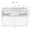
- FIGS. 12 through 18 are cross-sectional views for illustrating a method of manufacturing an inkjet printhead according to another embodiment of the present disclosure. For the sake of brevity, only those aspects that are substantially different from those of the previously described embodiments will be the primary focus of the following descriptions.
- the insulating layer 112 , the heaters 114 , the electrodes 116 , the passivation layer 118 , and the anti-cavitation layer 119 are formed on the substrate 110 .
- Such processes were previously described, and thus a detailed description is not repeated.
- the glue material layer 121 ′ which may include a negative type photosensitive resin, a PAG and a crosslink inhibitor, formed on the passivation layer 118 , is exposed.
- the cross linkage of the photosensitive resin is generated in the exposed part 121 a of the glue material layer 121 ′ as a result of the exposure.
- the photosensitive resin included in the glue material layer 121 ′ and a photosensitive resin included in a chamber material layer may be developed using different developing solutions.
- the glue material layer 121 ′ may be formed, for example, by coating a liquid-type photosensitive material on the passivation layer 118 or by laminating the photosensitive dry film on the passivation layer 118 .
- the chamber material layer (not shown), which may include a negative type photosensitive resin and PAG may be formed on the glue material layer 121 ′. Such chamber material layer may be exposed and developed, thereby forming the chamber layer 120 .
- the chamber material layer may be formed, for example, by laminating a photosensitive dry film which may include a negative type photosensitive resin and PAG, on the glue material layer 121 ′. Again, as described above, the photosensitive resin included in the chamber material layer and the photosensitive resin included in the glue material layer 121 may be developed using different developing solutions.
- So formed chamber layer 120 may include a plurality of ink chambers 122 and a plurality of restrictors 124 . According to an embodiment, both exposing processes for the glue material layer 121 ′ and for the chamber material layer may be performed simultaneously.
- the nozzle material layer 130 is formed on the chamber layer 120 .
- the nozzle material layer 130 ′ may be formed, for example, by laminating a photosensitive dry film, which may include a negative type photosensitive resin and PAG, on the chamber layer 120 .
- the photosensitive resin included in the nozzle material layer 130 ′ may be the same as the photosensitive resin included in the glue material layer 121 ′.
- the exposing process for the nozzle material layer 130 ′ is performed.
- the exposing process for the nozzle material layer 130 ′ may be performed, for example, by preparing the photomask 170 , on which a nozzle pattern is formed, above the nozzle material layer 130 ′, and by irradiating UV rays having a predetermined wavelength onto the photomask 170 .
- cross linkage of the photosensitive resin may be generated in the exposed part 130 a of the nozzle material layer 130 ′.
- substantially no cross linkage of the photosensitive resin occurs in the glue material layer 121 ′ due to the crosslink inhibitor included in the glue material layer 121 ′.
- the nozzle material layer 130 ′ and the glue material layer 121 ′ may be developed using a developing solution.
- the developing of the nozzle material layer 130 ′ and developing of the glue material layer 121 ′ may be sequentially performed.
- the non-exposed part 130 b of the nozzle material layer 130 ′ (see FIG. 16 ) and the non-exposed part 121 b of the glue material layer 121 ′ (see FIG. 15 ), in both of which no cross linkage had occurred, may be removed.
- the nozzle layer 130 having the nozzles 132 is formed on the chamber layer 120 , and the glue layer 121 is formed between the passivation layer 118 and the chamber layer 120 as depicted in FIG. 17 .
- the manufacturing of the inkjet printhead could be considered completed.
- the ink feed hole 111 may be formed by etching so as to penetrate the substrate 110 from the lower surface thereof to the upper surface thereof.
Abstract
Description
Claims (25)
Applications Claiming Priority (2)
| Application Number | Priority Date | Filing Date | Title |
|---|---|---|---|
| KR10-2008-0108471 | 2008-11-03 | ||
| KR1020080108471A KR101522552B1 (en) | 2008-11-03 | 2008-11-03 | Inkjet printhead and method of manufacturing the same |
Publications (2)
| Publication Number | Publication Date |
|---|---|
| US20100110142A1 US20100110142A1 (en) | 2010-05-06 |
| US8083324B2 true US8083324B2 (en) | 2011-12-27 |
Family
ID=42130847
Family Applications (1)
| Application Number | Title | Priority Date | Filing Date |
|---|---|---|---|
| US12/489,599 Expired - Fee Related US8083324B2 (en) | 2008-11-03 | 2009-06-23 | Inkjet printhead and method of manufacturing the same |
Country Status (2)
| Country | Link |
|---|---|
| US (1) | US8083324B2 (en) |
| KR (1) | KR101522552B1 (en) |
Cited By (4)
| Publication number | Priority date | Publication date | Assignee | Title |
|---|---|---|---|---|
| US20170203569A1 (en) | 2016-01-19 | 2017-07-20 | Canon Kabushiki Kaisha | Liquid ejection head manufacturing method |
| US10322584B2 (en) | 2016-04-18 | 2019-06-18 | Canon Kabushiki Kaisha | Method for manufacturing liquid ejection head |
| US10625507B2 (en) | 2017-08-02 | 2020-04-21 | Canon Kabushiki Kaisha | Transfer method, manufacturing method of liquid ejection head, and frame jig |
| US10744771B2 (en) | 2017-09-06 | 2020-08-18 | Canon Kabushiki Kaisha | Method of manufacturing liquid ejection head and method of manufacturing structure |
Families Citing this family (3)
| Publication number | Priority date | Publication date | Assignee | Title |
|---|---|---|---|---|
| US9358783B2 (en) * | 2012-04-27 | 2016-06-07 | Hewlett-Packard Development Company, L.P. | Fluid ejection device and method of forming same |
| WO2016164041A1 (en) * | 2015-04-10 | 2016-10-13 | Hewlett-Packard Development Company, L.P. | Removing an inclined segment of a metal conductor while forming printheads |
| JP6765891B2 (en) * | 2016-07-29 | 2020-10-07 | キヤノン株式会社 | How to manufacture the structure |
Citations (11)
| Publication number | Priority date | Publication date | Assignee | Title |
|---|---|---|---|---|
| US7168787B2 (en) * | 2002-12-30 | 2007-01-30 | Samsung Electronics Co., Ltd. | Monolithic bubble-ink jet print head having anti-curing-deformation part and fabrication method thereof |
| US20070256301A1 (en) * | 2005-05-12 | 2007-11-08 | Samsung Electronics Co., Ltd. | Method of manufacturing inkjet printhead using crosslinked polymer |
| US20080303869A1 (en) * | 2007-06-07 | 2008-12-11 | Samsung Electronics Co., Ltd | Ink jet print head and manufacturing method thereof |
| US20090278898A1 (en) * | 2008-05-08 | 2009-11-12 | Samsung Electronics Co., Ltd. | Method of manufacturing inkjet printhead and inkjet printhead manufactured using the same |
| US20090309911A1 (en) * | 2008-01-08 | 2009-12-17 | Samsung Electronics Co., Ltd | Inkjet head chip and inkjet print head using the same |
| US20100033536A1 (en) * | 2008-08-11 | 2010-02-11 | Samsung Electronics Co., Ltd. | Inkjet printhead and method of manufacturing the same |
| US20100060695A1 (en) * | 2008-09-08 | 2010-03-11 | Samsung Electronics Co., Ltd. | Inkjet printhead and method of manufacturing the same |
| US20100118088A1 (en) * | 2008-11-07 | 2010-05-13 | Samsung Electronics Co., Ltd. | Inkjet printhead and method of manufacturing the same |
| US20100128091A1 (en) * | 2008-11-27 | 2010-05-27 | Samsung Electronics Co., Ltd. | Inkjet printhead and method of manufacturing the same |
| US20100165044A1 (en) * | 2008-12-31 | 2010-07-01 | Samsung Electronics Co., Ltd. | Inkjet prtinthead and method of manufacturing the same |
| US20110069121A1 (en) * | 2009-09-22 | 2011-03-24 | Samsung Electronics Co., Ltd. | Inkjet printhead and method of manufacturing the same |
Family Cites Families (4)
| Publication number | Priority date | Publication date | Assignee | Title |
|---|---|---|---|---|
| JP2881061B2 (en) * | 1992-01-13 | 1999-04-12 | 富士写真フイルム株式会社 | Thermal development color photosensitive material |
| IT1282672B1 (en) * | 1996-02-23 | 1998-03-31 | Grace W R & Co | THERMOPLASTIC MATERIAL FILMS WITH GAS BARRIER PROPERTY |
| KR20050112027A (en) * | 2004-05-24 | 2005-11-29 | 삼성전자주식회사 | Method of fabricating ink jet head having glue layer |
| KR100856412B1 (en) * | 2006-12-04 | 2008-09-04 | 삼성전자주식회사 | Method of manufacturing inkjet printhead |
-
2008
- 2008-11-03 KR KR1020080108471A patent/KR101522552B1/en not_active IP Right Cessation
-
2009
- 2009-06-23 US US12/489,599 patent/US8083324B2/en not_active Expired - Fee Related
Patent Citations (11)
| Publication number | Priority date | Publication date | Assignee | Title |
|---|---|---|---|---|
| US7168787B2 (en) * | 2002-12-30 | 2007-01-30 | Samsung Electronics Co., Ltd. | Monolithic bubble-ink jet print head having anti-curing-deformation part and fabrication method thereof |
| US20070256301A1 (en) * | 2005-05-12 | 2007-11-08 | Samsung Electronics Co., Ltd. | Method of manufacturing inkjet printhead using crosslinked polymer |
| US20080303869A1 (en) * | 2007-06-07 | 2008-12-11 | Samsung Electronics Co., Ltd | Ink jet print head and manufacturing method thereof |
| US20090309911A1 (en) * | 2008-01-08 | 2009-12-17 | Samsung Electronics Co., Ltd | Inkjet head chip and inkjet print head using the same |
| US20090278898A1 (en) * | 2008-05-08 | 2009-11-12 | Samsung Electronics Co., Ltd. | Method of manufacturing inkjet printhead and inkjet printhead manufactured using the same |
| US20100033536A1 (en) * | 2008-08-11 | 2010-02-11 | Samsung Electronics Co., Ltd. | Inkjet printhead and method of manufacturing the same |
| US20100060695A1 (en) * | 2008-09-08 | 2010-03-11 | Samsung Electronics Co., Ltd. | Inkjet printhead and method of manufacturing the same |
| US20100118088A1 (en) * | 2008-11-07 | 2010-05-13 | Samsung Electronics Co., Ltd. | Inkjet printhead and method of manufacturing the same |
| US20100128091A1 (en) * | 2008-11-27 | 2010-05-27 | Samsung Electronics Co., Ltd. | Inkjet printhead and method of manufacturing the same |
| US20100165044A1 (en) * | 2008-12-31 | 2010-07-01 | Samsung Electronics Co., Ltd. | Inkjet prtinthead and method of manufacturing the same |
| US20110069121A1 (en) * | 2009-09-22 | 2011-03-24 | Samsung Electronics Co., Ltd. | Inkjet printhead and method of manufacturing the same |
Cited By (6)
| Publication number | Priority date | Publication date | Assignee | Title |
|---|---|---|---|---|
| US20170203569A1 (en) | 2016-01-19 | 2017-07-20 | Canon Kabushiki Kaisha | Liquid ejection head manufacturing method |
| JP2017128006A (en) * | 2016-01-19 | 2017-07-27 | キヤノン株式会社 | Method of manufacturing liquid discharge head |
| US10343406B2 (en) | 2016-01-19 | 2019-07-09 | Canon Kabushiki Kaisha | Liquid ejection head manufacturing method |
| US10322584B2 (en) | 2016-04-18 | 2019-06-18 | Canon Kabushiki Kaisha | Method for manufacturing liquid ejection head |
| US10625507B2 (en) | 2017-08-02 | 2020-04-21 | Canon Kabushiki Kaisha | Transfer method, manufacturing method of liquid ejection head, and frame jig |
| US10744771B2 (en) | 2017-09-06 | 2020-08-18 | Canon Kabushiki Kaisha | Method of manufacturing liquid ejection head and method of manufacturing structure |
Also Published As
| Publication number | Publication date |
|---|---|
| KR20100049352A (en) | 2010-05-12 |
| KR101522552B1 (en) | 2015-05-26 |
| US20100110142A1 (en) | 2010-05-06 |
Similar Documents
| Publication | Publication Date | Title |
|---|---|---|
| US8083324B2 (en) | Inkjet printhead and method of manufacturing the same | |
| JP5356646B2 (en) | High resolution pattern formation method | |
| US8148049B2 (en) | Ink jet recording head and manufacturing method of the same | |
| KR101012898B1 (en) | Liquid discharge head producing method | |
| KR100818277B1 (en) | Method of manufacturing inkjet printhead | |
| US20100028812A1 (en) | Method of manufacturing inkjet printhead | |
| JP2003145780A (en) | Production method for ink-jet printing head | |
| JP4729730B2 (en) | Inkjet printhead manufacturing method | |
| US8904639B2 (en) | Method of producing liquid ejection head | |
| JP2005104156A (en) | Manufacturing method of ink-jet printhead | |
| JP2010023494A (en) | Processing method for board, manufacturing method of board for liquid discharging head, and manufacturing method for liquid discharging head | |
| US8104872B2 (en) | Inkjet printhead and method of manufacturing the same | |
| KR100856412B1 (en) | Method of manufacturing inkjet printhead | |
| US8277023B2 (en) | Inkjet printhead and method of manufacturing the same | |
| JP6242174B2 (en) | Manufacturing method of ink discharge head | |
| JP2008290413A (en) | Method for manufacturing liquid ejecting head | |
| KR20090114787A (en) | Ink jet print head and manufacturing method thereof | |
| JP4845692B2 (en) | Method for manufacturing liquid discharge head | |
| JP2020062809A (en) | Manufacturing method of liquid discharge head | |
| US8118403B2 (en) | Inkjet printhead and method of manufacturing the same | |
| US8147037B2 (en) | Inkjet printhead and method of manufacturing the same | |
| US20030132990A1 (en) | Inkjet recording head, recording apparatus including the inkjet recording head, and method for manufacturing the inkjet recording head | |
| KR20060025876A (en) | Ink-jet printer head and manufacturing methods thereof | |
| US8114578B2 (en) | Method of manufacturing photosensitive epoxy structure using photolithography process and method of manufacturing inkjet printhead using the method of manufacturing photosensitive epoxy structure | |
| KR100509481B1 (en) | Method for manufacturing monolithic inkjet printhead |
Legal Events
| Date | Code | Title | Description |
|---|---|---|---|
| AS | Assignment |
Owner name: SAMSUNG ELECTRONICS CO., LTD.,KOREA, REPUBLIC OF Free format text: ASSIGNMENT OF ASSIGNORS INTEREST;ASSIGNORS:KWON, MYONG-JONG;PARK, SUNG-JOON;LEE, JIN-WOOK;SIGNING DATES FROM 20090529 TO 20090612;REEL/FRAME:022861/0620 Owner name: SAMSUNG ELECTRONICS CO., LTD., KOREA, REPUBLIC OF Free format text: ASSIGNMENT OF ASSIGNORS INTEREST;ASSIGNORS:KWON, MYONG-JONG;PARK, SUNG-JOON;LEE, JIN-WOOK;SIGNING DATES FROM 20090529 TO 20090612;REEL/FRAME:022861/0620 |
|
| FEPP | Fee payment procedure |
Free format text: PAYOR NUMBER ASSIGNED (ORIGINAL EVENT CODE: ASPN); ENTITY STATUS OF PATENT OWNER: LARGE ENTITY |
|
| STCF | Information on status: patent grant |
Free format text: PATENTED CASE |
|
| FPAY | Fee payment |
Year of fee payment: 4 |
|
| AS | Assignment |
Owner name: S-PRINTING SOLUTION CO., LTD., KOREA, REPUBLIC OF Free format text: ASSIGNMENT OF ASSIGNORS INTEREST;ASSIGNOR:SAMSUNG ELECTRONICS CO., LTD;REEL/FRAME:041852/0125 Effective date: 20161104 |
|
| AS | Assignment |
Owner name: HP PRINTING KOREA CO., LTD., KOREA, REPUBLIC OF Free format text: CHANGE OF NAME;ASSIGNOR:S-PRINTING SOLUTION CO., LTD.;REEL/FRAME:047370/0405 Effective date: 20180316 |
|
| AS | Assignment |
Owner name: HP PRINTING KOREA CO., LTD., KOREA, REPUBLIC OF Free format text: CORRECTIVE ASSIGNMENT TO CORRECT THE DOCUMENTATION EVIDENCING THE CHANGE OF NAME PREVIOUSLY RECORDED ON REEL 047370 FRAME 0405. ASSIGNOR(S) HEREBY CONFIRMS THE CHANGE OF NAME;ASSIGNOR:S-PRINTING SOLUTION CO., LTD.;REEL/FRAME:047769/0001 Effective date: 20180316 |
|
| FEPP | Fee payment procedure |
Free format text: MAINTENANCE FEE REMINDER MAILED (ORIGINAL EVENT CODE: REM.); ENTITY STATUS OF PATENT OWNER: LARGE ENTITY |
|
| AS | Assignment |
Owner name: HP PRINTING KOREA CO., LTD., KOREA, REPUBLIC OF Free format text: CHANGE OF LEGAL ENTITY EFFECTIVE AUG. 31, 2018;ASSIGNOR:HP PRINTING KOREA CO., LTD.;REEL/FRAME:050938/0139 Effective date: 20190611 |
|
| AS | Assignment |
Owner name: HEWLETT-PACKARD DEVELOPMENT COMPANY, L.P., TEXAS Free format text: CONFIRMATORY ASSIGNMENT EFFECTIVE NOVEMBER 1, 2018;ASSIGNOR:HP PRINTING KOREA CO., LTD.;REEL/FRAME:050747/0080 Effective date: 20190826 |
|
| LAPS | Lapse for failure to pay maintenance fees |
Free format text: PATENT EXPIRED FOR FAILURE TO PAY MAINTENANCE FEES (ORIGINAL EVENT CODE: EXP.); ENTITY STATUS OF PATENT OWNER: LARGE ENTITY |
|
| STCH | Information on status: patent discontinuation |
Free format text: PATENT EXPIRED DUE TO NONPAYMENT OF MAINTENANCE FEES UNDER 37 CFR 1.362 |
|
| FP | Lapsed due to failure to pay maintenance fee |
Effective date: 20191227 |