JP2010023494A - Processing method for board, manufacturing method of board for liquid discharging head, and manufacturing method for liquid discharging head - Google Patents
Processing method for board, manufacturing method of board for liquid discharging head, and manufacturing method for liquid discharging head Download PDFInfo
- Publication number
- JP2010023494A JP2010023494A JP2009130797A JP2009130797A JP2010023494A JP 2010023494 A JP2010023494 A JP 2010023494A JP 2009130797 A JP2009130797 A JP 2009130797A JP 2009130797 A JP2009130797 A JP 2009130797A JP 2010023494 A JP2010023494 A JP 2010023494A
- Authority
- JP
- Japan
- Prior art keywords
- substrate
- layer
- liquid
- etching
- forming
- Prior art date
- Legal status (The legal status is an assumption and is not a legal conclusion. Google has not performed a legal analysis and makes no representation as to the accuracy of the status listed.)
- Granted
Links
- 239000007788 liquid Substances 0.000 title claims abstract description 122
- 238000004519 manufacturing process Methods 0.000 title claims abstract description 36
- 238000003672 processing method Methods 0.000 title claims abstract description 13
- 238000007599 discharging Methods 0.000 title abstract description 8
- 238000005530 etching Methods 0.000 claims abstract description 63
- 239000000463 material Substances 0.000 claims abstract description 54
- 238000000034 method Methods 0.000 claims abstract description 49
- 239000000758 substrate Substances 0.000 claims description 124
- 239000010931 gold Substances 0.000 claims description 12
- 230000005540 biological transmission Effects 0.000 claims description 9
- PCHJSUWPFVWCPO-UHFFFAOYSA-N gold Chemical compound [Au] PCHJSUWPFVWCPO-UHFFFAOYSA-N 0.000 claims description 8
- 229910052737 gold Inorganic materials 0.000 claims description 8
- 238000012545 processing Methods 0.000 claims description 8
- 229910052751 metal Inorganic materials 0.000 claims description 7
- 239000002184 metal Substances 0.000 claims description 7
- 239000010949 copper Substances 0.000 claims description 3
- 238000001039 wet etching Methods 0.000 claims description 3
- RYGMFSIKBFXOCR-UHFFFAOYSA-N Copper Chemical compound [Cu] RYGMFSIKBFXOCR-UHFFFAOYSA-N 0.000 claims description 2
- BQCADISMDOOEFD-UHFFFAOYSA-N Silver Chemical compound [Ag] BQCADISMDOOEFD-UHFFFAOYSA-N 0.000 claims description 2
- 238000002679 ablation Methods 0.000 claims description 2
- 229910052802 copper Inorganic materials 0.000 claims description 2
- 229910052709 silver Inorganic materials 0.000 claims description 2
- 239000004332 silver Substances 0.000 claims description 2
- 238000003754 machining Methods 0.000 abstract 1
- 239000010410 layer Substances 0.000 description 102
- XUIMIQQOPSSXEZ-UHFFFAOYSA-N Silicon Chemical compound [Si] XUIMIQQOPSSXEZ-UHFFFAOYSA-N 0.000 description 16
- 229910052710 silicon Inorganic materials 0.000 description 16
- 239000010703 silicon Substances 0.000 description 16
- 230000017525 heat dissipation Effects 0.000 description 13
- CNQCVBJFEGMYDW-UHFFFAOYSA-N lawrencium atom Chemical compound [Lr] CNQCVBJFEGMYDW-UHFFFAOYSA-N 0.000 description 11
- 238000010438 heat treatment Methods 0.000 description 10
- 229920005989 resin Polymers 0.000 description 9
- 239000011347 resin Substances 0.000 description 9
- 230000015572 biosynthetic process Effects 0.000 description 4
- 238000002360 preparation method Methods 0.000 description 4
- 239000011241 protective layer Substances 0.000 description 4
- WGTYBPLFGIVFAS-UHFFFAOYSA-M tetramethylammonium hydroxide Chemical compound [OH-].C[N+](C)(C)C WGTYBPLFGIVFAS-UHFFFAOYSA-M 0.000 description 4
- NTIZESTWPVYFNL-UHFFFAOYSA-N Methyl isobutyl ketone Chemical compound CC(C)CC(C)=O NTIZESTWPVYFNL-UHFFFAOYSA-N 0.000 description 3
- UIHCLUNTQKBZGK-UHFFFAOYSA-N Methyl isobutyl ketone Natural products CCC(C)C(C)=O UIHCLUNTQKBZGK-UHFFFAOYSA-N 0.000 description 3
- VYPSYNLAJGMNEJ-UHFFFAOYSA-N Silicium dioxide Chemical compound O=[Si]=O VYPSYNLAJGMNEJ-UHFFFAOYSA-N 0.000 description 3
- 238000009429 electrical wiring Methods 0.000 description 3
- 238000007789 sealing Methods 0.000 description 3
- 239000000243 solution Substances 0.000 description 3
- 235000001674 Agaricus brunnescens Nutrition 0.000 description 2
- 229920002614 Polyether block amide Polymers 0.000 description 2
- 229910052581 Si3N4 Inorganic materials 0.000 description 2
- 238000010521 absorption reaction Methods 0.000 description 2
- 239000013078 crystal Substances 0.000 description 2
- 238000010586 diagram Methods 0.000 description 2
- 239000007769 metal material Substances 0.000 description 2
- 238000007747 plating Methods 0.000 description 2
- 230000001681 protective effect Effects 0.000 description 2
- 238000001454 recorded image Methods 0.000 description 2
- HQVNEWCFYHHQES-UHFFFAOYSA-N silicon nitride Chemical compound N12[Si]34N5[Si]62N3[Si]51N64 HQVNEWCFYHHQES-UHFFFAOYSA-N 0.000 description 2
- 235000012431 wafers Nutrition 0.000 description 2
- 239000004952 Polyamide Substances 0.000 description 1
- 239000012670 alkaline solution Substances 0.000 description 1
- CSDREXVUYHZDNP-UHFFFAOYSA-N alumanylidynesilicon Chemical compound [Al].[Si] CSDREXVUYHZDNP-UHFFFAOYSA-N 0.000 description 1
- 229910052782 aluminium Inorganic materials 0.000 description 1
- XAGFODPZIPBFFR-UHFFFAOYSA-N aluminium Chemical compound [Al] XAGFODPZIPBFFR-UHFFFAOYSA-N 0.000 description 1
- WPPDFTBPZNZZRP-UHFFFAOYSA-N aluminum copper Chemical compound [Al].[Cu] WPPDFTBPZNZZRP-UHFFFAOYSA-N 0.000 description 1
- -1 aluminum silicon copper Chemical compound 0.000 description 1
- 238000009835 boiling Methods 0.000 description 1
- 230000005587 bubbling Effects 0.000 description 1
- 238000012663 cationic photopolymerization Methods 0.000 description 1
- 239000000919 ceramic Substances 0.000 description 1
- 238000006243 chemical reaction Methods 0.000 description 1
- 238000004891 communication Methods 0.000 description 1
- 238000012937 correction Methods 0.000 description 1
- 230000007797 corrosion Effects 0.000 description 1
- 238000005260 corrosion Methods 0.000 description 1
- 238000011161 development Methods 0.000 description 1
- 239000003814 drug Substances 0.000 description 1
- 230000000694 effects Effects 0.000 description 1
- 239000003822 epoxy resin Substances 0.000 description 1
- 239000004744 fabric Substances 0.000 description 1
- 239000000835 fiber Substances 0.000 description 1
- 239000011521 glass Substances 0.000 description 1
- 239000003999 initiator Substances 0.000 description 1
- 230000001678 irradiating effect Effects 0.000 description 1
- 239000010985 leather Substances 0.000 description 1
- 239000003595 mist Substances 0.000 description 1
- 239000000203 mixture Substances 0.000 description 1
- 230000000149 penetrating effect Effects 0.000 description 1
- 239000004033 plastic Substances 0.000 description 1
- 229920002647 polyamide Polymers 0.000 description 1
- 229920000647 polyepoxide Polymers 0.000 description 1
- 239000011342 resin composition Substances 0.000 description 1
- 238000004904 shortening Methods 0.000 description 1
- 235000012239 silicon dioxide Nutrition 0.000 description 1
- 239000000377 silicon dioxide Substances 0.000 description 1
- 229910052814 silicon oxide Inorganic materials 0.000 description 1
- 239000002904 solvent Substances 0.000 description 1
- MZLGASXMSKOWSE-UHFFFAOYSA-N tantalum nitride Chemical compound [Ta]#N MZLGASXMSKOWSE-UHFFFAOYSA-N 0.000 description 1
- 238000012360 testing method Methods 0.000 description 1
- 239000002023 wood Substances 0.000 description 1
Images


Classifications
-
- B—PERFORMING OPERATIONS; TRANSPORTING
- B41—PRINTING; LINING MACHINES; TYPEWRITERS; STAMPS
- B41J—TYPEWRITERS; SELECTIVE PRINTING MECHANISMS, i.e. MECHANISMS PRINTING OTHERWISE THAN FROM A FORME; CORRECTION OF TYPOGRAPHICAL ERRORS
- B41J2/00—Typewriters or selective printing mechanisms characterised by the printing or marking process for which they are designed
- B41J2/005—Typewriters or selective printing mechanisms characterised by the printing or marking process for which they are designed characterised by bringing liquid or particles selectively into contact with a printing material
- B41J2/01—Ink jet
- B41J2/135—Nozzles
- B41J2/16—Production of nozzles
- B41J2/1601—Production of bubble jet print heads
- B41J2/1603—Production of bubble jet print heads of the front shooter type
-
- B—PERFORMING OPERATIONS; TRANSPORTING
- B41—PRINTING; LINING MACHINES; TYPEWRITERS; STAMPS
- B41J—TYPEWRITERS; SELECTIVE PRINTING MECHANISMS, i.e. MECHANISMS PRINTING OTHERWISE THAN FROM A FORME; CORRECTION OF TYPOGRAPHICAL ERRORS
- B41J2/00—Typewriters or selective printing mechanisms characterised by the printing or marking process for which they are designed
- B41J2/005—Typewriters or selective printing mechanisms characterised by the printing or marking process for which they are designed characterised by bringing liquid or particles selectively into contact with a printing material
- B41J2/01—Ink jet
- B41J2/135—Nozzles
- B41J2/16—Production of nozzles
- B41J2/1621—Manufacturing processes
- B41J2/1626—Manufacturing processes etching
- B41J2/1629—Manufacturing processes etching wet etching
-
- B—PERFORMING OPERATIONS; TRANSPORTING
- B41—PRINTING; LINING MACHINES; TYPEWRITERS; STAMPS
- B41J—TYPEWRITERS; SELECTIVE PRINTING MECHANISMS, i.e. MECHANISMS PRINTING OTHERWISE THAN FROM A FORME; CORRECTION OF TYPOGRAPHICAL ERRORS
- B41J2/00—Typewriters or selective printing mechanisms characterised by the printing or marking process for which they are designed
- B41J2/005—Typewriters or selective printing mechanisms characterised by the printing or marking process for which they are designed characterised by bringing liquid or particles selectively into contact with a printing material
- B41J2/01—Ink jet
- B41J2/135—Nozzles
- B41J2/16—Production of nozzles
- B41J2/1621—Manufacturing processes
- B41J2/1632—Manufacturing processes machining
- B41J2/1634—Manufacturing processes machining laser machining
-
- B—PERFORMING OPERATIONS; TRANSPORTING
- B41—PRINTING; LINING MACHINES; TYPEWRITERS; STAMPS
- B41J—TYPEWRITERS; SELECTIVE PRINTING MECHANISMS, i.e. MECHANISMS PRINTING OTHERWISE THAN FROM A FORME; CORRECTION OF TYPOGRAPHICAL ERRORS
- B41J2/00—Typewriters or selective printing mechanisms characterised by the printing or marking process for which they are designed
- B41J2/005—Typewriters or selective printing mechanisms characterised by the printing or marking process for which they are designed characterised by bringing liquid or particles selectively into contact with a printing material
- B41J2/01—Ink jet
- B41J2/135—Nozzles
- B41J2/16—Production of nozzles
- B41J2/1621—Manufacturing processes
- B41J2/1635—Manufacturing processes dividing the wafer into individual chips
-
- B—PERFORMING OPERATIONS; TRANSPORTING
- B41—PRINTING; LINING MACHINES; TYPEWRITERS; STAMPS
- B41J—TYPEWRITERS; SELECTIVE PRINTING MECHANISMS, i.e. MECHANISMS PRINTING OTHERWISE THAN FROM A FORME; CORRECTION OF TYPOGRAPHICAL ERRORS
- B41J2/00—Typewriters or selective printing mechanisms characterised by the printing or marking process for which they are designed
- B41J2/005—Typewriters or selective printing mechanisms characterised by the printing or marking process for which they are designed characterised by bringing liquid or particles selectively into contact with a printing material
- B41J2/01—Ink jet
- B41J2/135—Nozzles
- B41J2/16—Production of nozzles
- B41J2/1621—Manufacturing processes
- B41J2/1637—Manufacturing processes molding
- B41J2/1639—Manufacturing processes molding sacrificial molding
Abstract
Description
本発明は、基板の加工方法、液体吐出ヘッドに使用される液体吐出ヘッド用基板および液体吐出ヘッドの製造方法に関する。 The present invention relates to a substrate processing method, a liquid discharge head substrate used in a liquid discharge head, and a method of manufacturing a liquid discharge head.
吐出口から液体を吐出する液体吐出装置の一例として、液体であるインクを記録媒体に吐出して記録を行うインクジェット記録装置がある。液体吐出装置は液体を吐出するための液体吐出ヘッドを備えている。 As an example of a liquid ejecting apparatus that ejects liquid from an ejection port, there is an ink jet recording apparatus that performs recording by ejecting liquid ink onto a recording medium. The liquid ejection apparatus includes a liquid ejection head for ejecting liquid.
液体吐出ヘッドは、ノズル材が一面に形成された基板を有する。ノズル材には、液体を吐出する吐出口やノズルが形成されている。基板にはノズル材に液体を供給する液体供給口が形成されている。また、当該基板には液体を吐出するエネルギーを発生する吐出エネルギー発生素子が設けられている。液体吐出ヘッドは、吐出エネルギー発生素子が発するエネルギーによって液体を吐出する。 The liquid discharge head includes a substrate on which a nozzle material is formed. In the nozzle material, a discharge port and a nozzle for discharging a liquid are formed. A liquid supply port for supplying a liquid to the nozzle material is formed on the substrate. The substrate is provided with a discharge energy generating element that generates energy for discharging the liquid. The liquid discharge head discharges liquid by energy generated by the discharge energy generating element.
液体吐出ヘッドとしては、基板に対し垂直な方向に液体を吐出する方式のインクジェットヘッド(以下、サイドシュータ型ヘッドと呼ぶ。)が知られている。サイドシュータ型ヘッドでは、基板に貫通穴(スルーホール)である液体供給口が設けられており、この液体供給口を介して液体吐出ヘッドに液体が供給される。この液体供給口を形成するために基板加工の技術が用いられている。 As a liquid discharge head, an ink jet head (hereinafter referred to as a side shooter type head) that discharges liquid in a direction perpendicular to a substrate is known. In the side shooter type head, a liquid supply port which is a through hole (through hole) is provided in the substrate, and the liquid is supplied to the liquid discharge head through the liquid supply port. In order to form the liquid supply port, a substrate processing technique is used.
特許文献1には、サイドシュータ型の液体吐出ヘッドの製造方法が開示されている。特許文献1に記載の液体吐出ヘッドの製造方法は、スルーホールの開口径のばらつきを防ぐために、以下の(A)〜(F)の工程を有している。 Patent Document 1 discloses a method for manufacturing a side shooter type liquid discharge head. The method of manufacturing a liquid discharge head described in Patent Document 1 includes the following steps (A) to (F) in order to prevent variation in the opening diameter of the through hole.
(A)基板一面のスルーホール形成部位に基板材料に対して選択的にエッチングが可能な犠牲層を形成する工程
(B)基板に形成された犠牲層を被覆するように耐エッチング性を有するエッチングストップ層を形成する工程
(C)犠牲層に対応した開口部を有するエッチングマスク層を前記基板の前記一面と対向する側の前記面に形成する工程
(D)前記開口部より犠牲層が露出するまで基板を結晶軸異方性エッチングにてエッチングする工程
(E)エッチングにより露出した部分より犠牲層をエッチングして除去する工程
(F)エッチングストップ層の一部を除去しスルーホールを形成する工程。
(A) A step of forming a sacrificial layer that can be selectively etched with respect to the substrate material in a through hole forming portion on one surface of the substrate. (B) Etching having etching resistance so as to cover the sacrificial layer formed on the substrate. Step of forming stop layer (C) Step of forming an etching mask layer having an opening corresponding to the sacrificial layer on the surface opposite to the one surface of the substrate (D) The sacrificial layer is exposed from the opening (E) A step of etching and removing a sacrificial layer from a portion exposed by etching (F) A step of removing a part of the etching stop layer and forming a through hole .
特許文献2では、液体吐出ヘッドの製造方法において、異方性エッチングを行う前に、基板にレーザー光で非貫通穴を形成することが記載されている。 Japanese Patent Application Laid-Open No. H10-228561 describes that in a method for manufacturing a liquid discharge head, a non-through hole is formed in a substrate with laser light before performing anisotropic etching.
特許文献1のように、エッチングによって基板に液体供給口を形成する場合、エッチングに時間を要し、生産効率が低下するという課題があった。 When the liquid supply port is formed in the substrate by etching as in Patent Document 1, the etching takes time and there is a problem that the production efficiency is lowered.
また、特許文献2に記載の液体吐出ヘッドの製造方法では、エッチングによって基板に液体供給口を形成する前に、基板の一面と対向する側の面にレーザー光で非貫通穴を形成する。しかし、レーザー光では、非貫通穴の深さを正確に制御することは困難である。 Further, in the method for manufacturing a liquid discharge head described in Patent Document 2, before forming a liquid supply port in the substrate by etching, a non-through hole is formed with a laser beam on the surface facing the one surface of the substrate. However, it is difficult to accurately control the depth of the non-through hole with laser light.
そのため、基板の一面側近傍に到達する穴を形成する場合、穴が貫通してしまう可能性がある。この場合、基板の一面側に設けられているノズル材がレーザー光によって損傷するという懸念がある。したがって、基板に、深い穴を安定的に形成することは困難である。 Therefore, when forming a hole that reaches the vicinity of one surface side of the substrate, the hole may penetrate. In this case, there is a concern that the nozzle material provided on the one surface side of the substrate is damaged by the laser light. Therefore, it is difficult to stably form deep holes in the substrate.
本発明の目的は上記背景技術の課題に鑑み、高い生産効率で安定的に、基板に穴を形成することができる方法を提供することである。また、本発明の他の目的は、当該方法を利用した、液体吐出ヘッドの製造方法を提供することである。 An object of the present invention is to provide a method capable of stably forming a hole in a substrate with high production efficiency in view of the problems of the background art. Another object of the present invention is to provide a method of manufacturing a liquid discharge head using the method.
本発明の目的は上記背景技術の課題に鑑み、高い生産効率で安定的に、基板に穴を形成することができる方法を提供することである。また、本発明の他の目的は、当該方法を利用した、液体吐出ヘッドの製造方法を提供することである。 An object of the present invention is to provide a method capable of stably forming a hole in a substrate with high production efficiency in view of the problems of the background art. Another object of the present invention is to provide a method of manufacturing a liquid discharge head using the method.
本発明の一例としての基板の加工方法は、一方の面側にレーザー光の透過を抑制することが可能な材料からなる層が設けられた基板を用意することと、前記基板の前記一方の面の裏面から前記一方の面に向って、レーザー光により前記基板に加工を行い、前記レーザー光を前記層に到達させることにより前記基板に孔を形成することと、前記裏面から前記孔を通じて前記基板に対してエッチングを行うことと、を有する。 The substrate processing method as an example of the present invention includes preparing a substrate provided with a layer made of a material capable of suppressing transmission of laser light on one surface side, and said one surface of the substrate The substrate is processed with a laser beam from the back surface to the one surface, and a hole is formed in the substrate by allowing the laser beam to reach the layer, and the substrate is formed from the back surface through the hole. Etching.
本発明の一例によれば、高い生産効率で安定的に、基板に穴を形成することができる。 According to an example of the present invention, holes can be formed in a substrate stably with high production efficiency.
本発明によれば、高い生産効率で安定的に、基板に穴を形成することができる方法およびこれを利用した液体吐出ヘッドの製造方法を提供することができる。 ADVANTAGE OF THE INVENTION According to this invention, the method which can form a hole in a board | substrate stably with high production efficiency, and the manufacturing method of a liquid discharge head using this can be provided.
以下、本発明の実施形態について図面を参照して説明する。 Embodiments of the present invention will be described below with reference to the drawings.
なお、以下の説明では、液体吐出ヘッドの一例としてインクジェット記録ヘッド(以下記録ヘッド)を例示して説明する。他の応用例として液体吐出ヘッドは、工業用途、医療用途等に応用が可能である。 In the following description, an ink jet recording head (hereinafter referred to as a recording head) will be described as an example of the liquid discharge head. As another application example, the liquid discharge head can be applied to industrial use, medical use, and the like.
また、同一の機能を有する構成には図面中同一の番号を付与し、その説明を省略する場合がある。なお記録ヘッドは、プリンタ、複写機、通信システムを有するファクシミリ、プリンタ部を有するワードプロセッサなどの装置、さらには各種処理装置と複合的に組み合わせた産業記録装置に搭載可能である。そして、この記録ヘッドを用いることによって、紙、糸、繊維、布帛、皮革、金属、プラスチック、ガラス、木材、セラミックスなど種々の記録媒体に記録を行うことができる。なお、本明細書内で用いられる「記録」とは、文字や図形などの意味を持つ画像を記録媒体に対して付与することだけでなく、パターンなどの意味を持たない画像を付与することも意味することとする。 In addition, configurations having the same functions may be given the same numbers in the drawings, and descriptions thereof may be omitted. The recording head can be mounted on an apparatus such as a printer, a copying machine, a facsimile having a communication system, a word processor having a printer unit, or an industrial recording apparatus combined with various processing apparatuses. By using this recording head, recording can be performed on various recording media such as paper, thread, fiber, fabric, leather, metal, plastic, glass, wood, and ceramics. Note that “recording” used in the present specification not only applies an image having a meaning such as a character or a figure to a recording medium but also an image having no meaning such as a pattern. I mean.
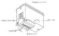
図3は本実施形態に係る液体吐出ヘッドユニットの斜視図である。液体吐出ヘッドユニット1は、被記録媒体等にインク等の液体を吐出する液体吐出ヘッド2と、インク等の液体を内部に収容しているケース部21と、記録動作等のための外部信号が入力される外部信号入力端子22と、を有している。液体吐出ヘッドユニット1は、インクジェット記録装置(不図示)に装着されると、外部信号入力端子22がインクジェット記録装置に電気的に接続されるように構成されている。 FIG. 3 is a perspective view of the liquid discharge head unit according to the present embodiment. The liquid discharge head unit 1 includes a liquid discharge head 2 that discharges a liquid such as ink onto a recording medium, a case portion 21 that stores a liquid such as ink, and an external signal for a recording operation. And an external signal input terminal 22 to be input. The liquid discharge head unit 1 is configured such that when the ink jet recording apparatus (not shown) is mounted, the external signal input terminal 22 is electrically connected to the ink jet recording apparatus.
液体吐出ヘッド2の両端部には、外部信号入力端子22に電気的に接続された電気的接続部が設けられ、電気的接続部を覆うように封止部材23が形成されている。電気的接続部を封止部材23で覆うことによって、液体吐出ヘッド2から吐出された液体が電気的接続部に接触することが防止されている。 At both ends of the liquid discharge head 2, an electrical connection portion electrically connected to the external signal input terminal 22 is provided, and a sealing member 23 is formed so as to cover the electrical connection portion. By covering the electrical connection portion with the sealing member 23, the liquid ejected from the liquid ejection head 2 is prevented from coming into contact with the electrical connection portion.
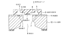
図4は図3に示した液体吐出ヘッドのA−A´線に沿った断面図である。液体吐出ヘッド2は、厚さ方向に貫通している供給口8が形成されたシリコン基板10と、シリコン基板10の一方の面である表面の上に設けられた樹脂製の流路形成部材3と、を有している。 4 is a cross-sectional view taken along the line AA ′ of the liquid discharge head shown in FIG. The liquid discharge head 2 includes a silicon substrate 10 in which a supply port 8 penetrating in the thickness direction is formed, and a resin flow path forming member 3 provided on the surface which is one surface of the silicon substrate 10. And have.
流路形成部材3には、吐出口5が形成され、吐出口5と供給口8とを連通するように流路6が形成されている。シリコン基板10の表面には、流路6内に配置された領域に、液体を吐出するために利用されるエネルギーを発生するエネルギー発生素子として窒化タンタルなどの発熱体で形成された発熱素子7が設けられている。更に全体を覆うように、窒化ケイ素などで形成された保護層11が設けられている。液体吐出ヘッド2では、発熱素子7が熱を発すると、発熱素子7に近接しているインク等の液体が瞬間的に加熱されて沸騰することで発生する発泡圧によって、吐出口5に近接している液体が吐出口5から吐出される。
A
流路形成部材3の、供給口8側の面には、放熱部材4が設けられていてもよい。放熱部材が設けられる場合には、放熱部材4は周囲を流路形成部材3に覆われることによって、流路形成部材3に保持されている。放熱部材4の供給口8側の端部は、流路形成部材3に覆われておらず、インクに直接接触する。放熱部材は熱伝導率が高い材料で形成され、本実施形態では、放熱部材4は、熱伝導率が高く、かつ、延性および展性に富み、耐食性に優れた金(Au)で形成されている。
A
図5は図3に示した液体吐出ヘッドユニット1の液体吐出ヘッドの部分を示した正面図である。図5では、説明の便宜上、封止部材23は省略した。 FIG. 5 is a front view showing a portion of the liquid discharge head of the liquid discharge head unit 1 shown in FIG. In FIG. 5, the sealing member 23 is omitted for convenience of explanation.
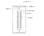
発熱素子7および吐出口5は2列に配列されており、液体吐出ヘッド2の表面側の、発熱素子7の配列方向における両端部には、外部信号入力端子22(図3参照)に電気的に接続された電気的接続部である複数の電極パッド9がそれぞれ設けられている。また、液体吐出ヘッド2の表面側には、電極パッド9に電気的に接続された電気配線(不図示)が設けられており、外部信号入力端子22から電極パッド9に伝達された外部信号は、電気配線を介して発熱素子7などに伝達される。
The
放熱部材4は、発熱素子7の2つの列の間に、発熱素子7の配列方向に沿って直線状に延びるように形成されている。したがって、各発熱素子7の近傍には放熱部材4が配置されており、発熱素子7が発した熱は、放熱部材4によって吐出口5の配列方向に拡散される。このように、液体吐出ヘッド2では、発熱素子7が発した熱が発熱素子7の近傍の部分に蓄積されずに拡散されるため、温度上昇が抑制される。
The
更に、放熱部材4は、液体吐出ヘッド2の両端部の電極パッド9に接続されており、発熱素子7が発した熱は、放熱部材7と電極パッド9とを介して、液体吐出ヘッドユニット1の外部信号入力端子22側へ放出される。これにより、液体吐出ヘッド2の放熱性は向上する。
Further, the
また、放熱部材4は、液体に直接接触する位置に配置されているため、効率的にインク等の液体の放熱をすることができる。これにより、インク等の液体の温度が上昇することが良好に抑制されるため、インクが変質することを防止することができる。
Moreover, since the
以上述べたように、本実施形態に係る液体吐出ヘッドユニット1は、発熱素子2が発した熱を放熱部材4が液体吐出ヘッド2から放出するので、高い放熱性を有する。
(第1の実施形態)
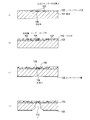
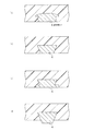
以下では、本発明の一例の基板の加工方法の一例としての液体吐出ヘッド用基板の製造方法を説明する。図1(a)〜(d)は、本実施例に係る基板に穴を形成する方法を示すステップ図である。
As described above, the liquid discharge head unit 1 according to the present embodiment has high heat dissipation because the
(First embodiment)
Hereinafter, a method for manufacturing a substrate for a liquid discharge head as an example of a substrate processing method according to an example of the present invention will be described. 1A to 1D are step diagrams showing a method for forming a hole in a substrate according to this embodiment.
基板に穴を形成する方法は、準備工程、レーザーストップ層形成工程、先導穴形成工程、及びエッチング工程を有している。 The method of forming holes in the substrate includes a preparation process, a laser stop layer forming process, a leading hole forming process, and an etching process.
準備工程では基板101を準備する(図1(a)参照。)。基板101としては、例えばシリコン基板を用いることが出来る。基板101の一面には、液体を吐出するエネルギーを発生する吐出エネルギー発生素子103が形成されている。
In the preparation step, the substrate 101 is prepared (see FIG. 1A). As the substrate 101, for example, a silicon substrate can be used. A discharge
また、基板101の一面には犠牲層106が形成されている。犠牲層106は、基板101の一面であって、後の工程で貫通穴が形成される部分に設けられている。犠牲層106としては、アルミ、アルミシリコン、アルミ銅、またはアルミシリコン銅など、アルカリ溶液に対してエッチング速度の速い材料を用いることが好ましい。
A
後述のレーザーストップ層形成工程を実施する前に、吐出エネルギー発生素子103、犠牲層106、及び基板101の一面を覆うように、エッチングストップ層102を形成することが望ましい。エッチングストップ層102は、ウェットエッチングに使用されるエッチング液に対する耐性(耐エッチング性)を有する材料からなり、吐出エネルギー発生素子103を保護する保護層として機能する。エッチングストップ層102は酸化珪素や窒化珪素などから成る。
It is desirable to form the
レーザーストップ層形成工程では、基板101の一面側に、レーザー光の透過を抑制するレーザーストップ層108を形成する(図1(b)参照。)。具体的には、基板101の一面側であって、後の工程で先導穴が形成される部分に、レーザーストップ層108を形成する。
In the laser stop layer forming step, a
レーザーストップ層108は基板101に設けられた犠牲層106に対応して設けられており、対応する犠牲層106の幅と同程度に形成される。
The
レーザーストップ層108は、レーザー光の透過を抑制し、レーザー光に対して耐性を有する層である。レーザーストップ層108は、後の工程で使用するレーザー光の吸収率が、基板におけるレーザー光の吸収率より十分に低い材料であれば良い。そのような材料として、金(Au)、銀(Ag)、及び銅(Cu)などの金属材料が挙げられる。このような金属材料はめっき法で形成することができる。
The
液体吐出用基板では、基板101の一面側に、配線層107と材料層であるノズル材110とをさらに形成する。配線層107は、吐出エネルギー発生素子103に電力を供給するために設けられる。また、ノズル材110は、液体を吐出するための吐出口と、当該吐出口と連通したノズルと、を有している。レーザーストップ層108は、材料層であるノズル材に覆われる。
In the liquid discharge substrate, a
先導穴形成工程では、基板101の一面と対向する側の面からレーザー光を照射して、当該面からレーザーストップ層108に到達する孔(以下、先導穴109と呼ぶ。)を形成する(図1(c)参照。)。
In the leading hole forming step, a laser beam is irradiated from the surface facing one surface of the substrate 101 to form a hole (hereinafter referred to as a leading hole 109) that reaches the
具体的には、基板101の一面と対向する側の面に開口部を有するエッチングマスク層105を形成し、当該開口部を通じて基板101にレーザー光を照射する。先導穴形成工程では、レーザー光を用いたアブレーション加工によって、先導穴109が形成される。
Specifically, an
エッチングマスク層105は、基板101の一面側に設けられたレーザーストップ層108に対応した開口部を有している。エッチングマスク層105としては、ポリエーテルアミド樹脂を用いることができる。
The
レーザーストップ層108はレーザー光の透過を十分に抑制するため、実質的に加工されず、レーザー光を反射する。そのため、レーザー光の出力を正確に調整する必要はなく、容易に先導穴109を形成することができる。
Since the
また、レーザー光がレーザーストップ層108を通過しないため、基板101の一面側に形成されている材料層であるノズル材110の損傷を防ぐことが出来る。
Further, since laser light does not pass through the
レーザー光としては、YAGレーザーの基本波(波長1064nm)を用いることができる。レーザー光の周波数は適切な値に設定される。本実施形態では、レーザーストップ層108として金(Au)を用いる。金は、YAGレーザーの基本波である1064nmの波長を有するレーザー光の吸収率が約2%と低く、レーザー光に対して耐性を有している。
As the laser light, a fundamental wave (wavelength 1064 nm) of a YAG laser can be used. The frequency of the laser beam is set to an appropriate value. In this embodiment, gold (Au) is used as the
それに対して、基板101として用いられるシリコンは、YAGレーザーの基本波を10%以上吸収する。そのため、レーザー光が照射されると、シリコン基板が削られて、先導穴109が形成される。
In contrast, silicon used as the substrate 101 absorbs 10% or more of the fundamental wave of the YAG laser. Therefore, when the laser beam is irradiated, the silicon substrate is scraped to form the leading
エッチング工程では、異方性エッチングによって、先導穴109の径を所望の大きさに広げる(図1(d)参照。)。具体的には、エッチングマスク層105をエッチング液に対する保護膜として、エッチングにより先導穴109を所望の径になるまで広げる。このようにして、基板101に所望の径の、供給口としての穴112を形成することができる。
In the etching process, the diameter of the leading
エッチング液としては、水酸化テトラメチルアンモニウム(TMAH)を用いることができる。先導穴109の底部近傍に位置するエッチングストップ層102は耐エッチング性を有しているため、エッチング液から吐出エネルギー発生素子103やノズル材110などを保護する機能を有する。
As an etchant, tetramethylammonium hydroxide (TMAH) can be used. Since the
先導穴形成工程において、レーザー光のビーム径を円形にすることは困難であるため、先導穴109の口径を円形に成形することは難しい。また、レーザー光で形成した先導穴109の側面には凸凹が形成されてしまう。さらに、レーザー光で、径の大きい先導穴109を形成するには、多大な時間を要する。
In the leading hole forming step, it is difficult to make the beam diameter of the laser light circular, so it is difficult to shape the diameter of the leading
そのため、レーザー光で径の小さい先導穴109を形成した後に、エッチング工程において、先導穴109の径を広げることにより、所望の径の穴112を安定的に形成することができる。また、エッチング液が先導穴109に入り込むため、異方性エッチングに要する時間(AE時間)が大幅に削減され、生産効率が向上する。
Therefore, after forming the leading
基板101に形成された穴112を液体吐出ヘッドの液体供給口として用いる場合、穴112の底部近傍に残っている犠牲層106及びエッチングストップ層102の一部を除去すれば良い。
When the
図1では、基板101に形成する穴112は1つのみ示されているが、複数の穴を同時に形成しても良い。
In FIG. 1, only one
上記実施形態では、基板101の一面側に材料層としてノズル材が形成される場合について説明したが、材料層はノズル材に限定されない。材料層としては、例えば樹脂層が挙げられる。本発明によれば、先導穴形成工程において、レーザーストップ層を覆う材料層をレーザー光から保護することができる。
(第2の実施形態)
次に、第1実施形態に係る基板の製造方法を利用した、液体吐出ヘッドの製造方法について詳細に説明する。液体吐出ヘッドとしては、液体であるインクを吐出して記録を行うインクジェットヘッドや、医療分野において液状薬剤を霧状として肺吸入させる際に使用される吸入装置などで液体を微小な液滴として噴霧吐出するヘッドなどが挙げられる。
In the above embodiment, the case where the nozzle material is formed as a material layer on one surface side of the substrate 101 has been described, but the material layer is not limited to the nozzle material. An example of the material layer is a resin layer. According to the present invention, the material layer covering the laser stop layer can be protected from the laser beam in the lead hole forming step.
(Second Embodiment)
Next, a manufacturing method of the liquid ejection head using the manufacturing method of the substrate according to the first embodiment will be described in detail. As the liquid ejection head, the liquid is sprayed as fine droplets by an inkjet head that performs recording by ejecting ink that is liquid, or an inhalation device that is used when inhaling a liquid medicine as a mist in the medical field. Examples include a discharge head.
図2(a)〜(f)は、本実施形態に係る液体吐出ヘッドの製造方法を示すステップ図である。液体吐出ヘッドの製造方法は、準備工程、配線工程、レーザーストップ層形成工程、ノズル材形成工程、先導穴形成工程、及びエッチング工程を有している。 2A to 2F are step diagrams illustrating a method for manufacturing a liquid ejection head according to the present embodiment. The manufacturing method of the liquid discharge head includes a preparation process, a wiring process, a laser stop layer forming process, a nozzle material forming process, a leading hole forming process, and an etching process.
まず、準備工程として基板101を準備する(図2(a)参照)。基板101の一面には、液体吐出ヘッドから液体を吐出するエネルギーを発生するための吐出エネルギー発生素子103が形成されている。吐出エネルギー発生素子103は、基板101にどのように配置されていても良い。
First, the substrate 101 is prepared as a preparation process (see FIG. 2A). On one surface of the substrate 101, an ejection
吐出エネルギー発生素子103としては、例えばヒータを用いることが出来る。ヒータの一例として、電熱変換素子(TaN)が挙げられる。なお、吐出エネルギー発生素子103は入力電極(不図示)と電気的に接続されている。この入力電極を介して、吐出エネルギー発生素子を駆動させるための制御信号が送られる。
As the ejection
本実施形態では、基板101として結晶軸(100)のシリコン基板を用いる。また、基板101の厚みは625μm程度に形成されている。基板101の一面側には犠牲層106が形成されている。また、吐出エネルギー発生素子103及び犠牲層106の形成場所及び材料は、第1の実施形態と同様である。また、基板101の一面と対向する側の面は、酸化膜104で覆われている。
In this embodiment, a silicon substrate having a crystal axis (100) is used as the substrate 101. The thickness of the substrate 101 is about 625 μm. A
第1の実施形態と同様に、レーザーストップ層形成工程を実施する前に、基板101の一面側を覆うエッチングストップ層102を形成することが望ましい。エッチングストップ層102は、耐エッチング性を有する材料からなる。
As in the first embodiment, it is desirable to form an
次に、配線層形成工程及びレーザーストップ層形成工程を実施する(図2(b)参照)。配線層形成工程では、吐出エネルギー発生素子103に電力を供給するための配線層107を、基板101の一面側に形成する。配線層107はめっき法によってパターニングすることができる。配線層107としては、例えば金(Au)のような金属を用いることができる。
Next, a wiring layer forming step and a laser stop layer forming step are performed (see FIG. 2B). In the wiring layer forming step, a
また、レーザーストップ層形成工程では、基板101の一面側、つまりエッチングストップ層102の一面にレーザーストップ層108を形成する。レーザーストップ層形成工程は、第1の実施形態と同様に形成することができる。
In the laser stop layer forming step, the
レーザーストップ層108と配線層107とを同種の金属にすることも好ましい態様の1つである。これにより、配線層形成工程とレーザーストップ工程とを、同時に実施することができ、製造時間の短縮を図ることができる。
It is also a preferable aspect that the
配線層形成工程とレーザーストップ層形成工程とを同時に行う場合、配線層107及びレーザーストップ層108の厚さは、0.5μm以上5.0μm以下であることが好ましい。これは、配線層107の電気抵抗を小さくし、さらに後の工程で形成するノズル材の表面(吐出口が形成される側の面。)を平坦にするためである。
When the wiring layer forming step and the laser stop layer forming step are performed simultaneously, the thickness of the
すなわち、配線層107の厚さが0.5μm未満の場合、配線抵抗が高くなる。また、配線層107及びレーザーストップ層108の厚さが5.0μmより厚い場合、ノズル材の表面に凹凸が形成されてしまう。ノズル材表面の凹凸は、液体の吐出性能を低下させる一要因となる。
That is, when the thickness of the
次に、ノズル材形成工程として、基板101の一面側にノズル材110を形成する(図2(c)参照)。ノズル材110には液体吐出ヘッドが液体を吐出するための吐出口202、及び吐出口202と連通したノズル203が形成される。
Next, as a nozzle material forming step, the nozzle material 110 is formed on one surface side of the substrate 101 (see FIG. 2C). The nozzle material 110 is formed with a
具体的には、まず、基板101の一面側であって、ノズルとなるべき部分に型材料201を積層する。型材料201としてはポジ型レジストを用いることができる。その後、ノズル材110である被覆感光性樹脂を、基板101の一面側に塗布する。吐出口202は、ノズル材110を露光、現像することで形成することができる。
Specifically, first, the
ノズル材形成工程は、上記方法に限定されず、任意の公知の方法によって形成することができる。 A nozzle material formation process is not limited to the said method, It can form by arbitrary well-known methods.
次に、先導穴形成工程として、基板101の一面と対向する側の面からレーザー光を照射して、当該面からレーザーストップ層108に到達する先導穴109を形成する(図2(d)参照。)。先導穴形成工程は第1の実施形態と同様に実施することができる。
Next, as a leading hole forming step, laser light is irradiated from the surface facing the one surface of the substrate 101 to form a leading
本実施形態では、先導穴109の直径を約40μmとした。先導穴109の直径は、約5μm以上、100μm以下であることが望ましい。これは、直径が小さすぎると、後に実施するエッチング工程においてエッチング液が先導穴109に入り難くなり、直径が大きすぎると、先導穴109の形成に多大な時間を要するためである。
In the present embodiment, the diameter of the leading
次に、エッチング工程として、異方性エッチングによって、先導穴109の径を所望の大きさまで広げ、液体供給口111を形成する(図2(e)参照。)。具体的にはまず、ポリエーテルアミド樹脂からなるエッチングマスク層105を保護膜として、エッチングマスク層105の開口部に露出した酸化膜104を除去する。
Next, as the etching process, the diameter of the leading
その後、第1の実施形態と同様に、基板101を異方性エッチングする。これにより、先導穴109は液体供給口111となる。
Thereafter, similarly to the first embodiment, the substrate 101 is anisotropically etched. As a result, the leading
その後、液体供給口111の底部近傍にある犠牲層106及びエッチングストップ層102の一部を除去することで、液体供給口111とノズル材110に形成されているノズル203とを連通させる(図2(f)参照。)。また、レーザーストップ層を除去することも可能である。
Thereafter, the
具体的には、犠牲層106は等方性エッチングにて除去される。また、エッチングストップ層102の犠牲層106に接触していた部分をエッチングによって除去する。そして、ノズル材110によって覆われている型材料201を除去することで、液体吐出ヘッドを製造することができる。型材料201は、遠紫外線を全面照射して、溶解除去することができる。
Specifically, the
本実施形態では、エッチング工程において異方性エッチングに要した時間(AE時間)は1時間であった。一方、先導穴形成工程を実施せず、エッチング工程のみで液体供給口を形成した場合、AE時間は16時間であった。このように、エッチング工程の前に、先導穴形成工程によって先導穴109を形成しておくことで、製造時間を大幅に短縮することが出来る。
In this embodiment, the time (AE time) required for anisotropic etching in the etching process was 1 hour. On the other hand, when the liquid supply port was formed only by the etching process without performing the lead hole forming process, the AE time was 16 hours. Thus, the manufacturing time can be significantly shortened by forming the leading
さらに、AE時間の短縮に伴い、液体供給口111の径は小さくなる。そのため、基板101に複数の液体供給口111を形成する場合、それぞれの液体供給口111間の間隔を狭くすることができる。したがって、液体吐出ヘッドのサイズを小さくすることができる。
Furthermore, as the AE time is shortened, the diameter of the
上記の実施形態では、基板単体を図示して、液体吐出用基板の製造方法を説明した。実際には、基板101はウエハ単位で製造されることが好ましい。また、上述の工程は、可能な限りその順番を入れ替えても構わない。 In the above embodiment, the method for manufacturing the liquid discharge substrate has been described with the substrate alone illustrated. Actually, it is preferable that the substrate 101 is manufactured in units of wafers. Further, the order of the above steps may be changed as much as possible.
以上、本発明の望ましい実施形態について提示し、詳細に説明したが、本発明は上記実施例に限定されるものではなく、要旨を逸脱しない限り、さまざまな変更及び修正が可能であることを理解されたい。
(第3の実施形態)
図6(a)は、図4に示した液体吐出ヘッドの放熱部材4の部分を示した拡大断面図である。放熱部材4はキノコ形状に形成されており、流路形成部材3に覆われた傘の部分が係止部となって、流放熱部材4が流路形成部材3から外れることを妨げている。したがって、供給口8から流路6に流れ込む液体から放熱部材4に加わる力などによって、放熱部材4が流路形成部材3から外れることを防止できる。
As mentioned above, although preferred embodiment of this invention was shown and described in detail, it understands that this invention is not limited to the said Example, A various change and correction are possible unless it deviates from the summary. I want to be.
(Third embodiment)
FIG. 6A is an enlarged cross-sectional view showing a portion of the
放熱部材は、図6(a)に示すようなキノコ形状に限らず、放熱部材4が流路形成部材3から外れることを妨げる係止部を備えていればよい。たとえば、図6(b)に示すような、流路形成部材の表面から内部にかけて広がるテーパ形状の場合にも、テーパ形状の側面が係止部となって放熱部材が流路形成部材から外れることを防止できる。また、図6(c)に示すように、放熱部材の、流路形成部材の表面に配置された部分を広く形成して、放熱部材の、液体に接触する部分の面積を増大させることによって、放熱性能を向上させることも可能である。また、図6(d)に示すように、放熱部材を流路形成部材の表面から突出するように形成して、放熱部材の、液体に接触する部分の面積を増大させることも可能である。
The heat radiating member is not limited to the mushroom shape as shown in FIG. 6A, and it is only necessary to include a locking portion that prevents the
次に、図7を参照して本実施形態に係る液体吐出ヘッドの製造方法について説明する。図7は本実施形態に係る液体吐出ヘッドの製造過程における断面図である。なお、図7においては、1つの液体吐出ヘッド2について示したが、実際にはウエハ単位で加工を行った後にダイシングにより個々の液体吐出ヘッド2に切り分ける。 Next, a manufacturing method of the liquid discharge head according to the present embodiment will be described with reference to FIG. FIG. 7 is a cross-sectional view in the process of manufacturing the liquid ejection head according to the present embodiment. In FIG. 7, one liquid discharge head 2 is shown, but in actuality, after processing in units of wafers, the individual liquid discharge heads 2 are separated by dicing.
まず、図7(a)に示すように、表面に発熱素子7およびエッチング犠牲層12が形成され、更に表面の全体を覆うように保護層11が形成されたシリコン基板10を用意する。シリコン基板10の他方の面である裏面には、エッチングマスクである二酸化ケイ素層13とポリアミド層14とが形成されている。発熱素子7には、電極パッド9に電気配線を介して電気的に接続された制御信号入力電極(不図示)が設けられている。シリコン基板10には、結晶方位が(100)で、厚さ625μmのものが用いられている。
First, as shown in FIG. 7A, a silicon substrate 10 is prepared in which a
次に、図7(b)に示すように、シリコン基板10の表面側のエッチング犠牲層12に対向する位置に金属層である放熱部材4を形成する。放熱部材4は金によって厚さが約4μmで、供給口8側の端部の幅が約40μmになるように形成した。
Next, as shown in FIG. 7B, a
放熱部材は、厚く形成されるほど熱伝導性が高くなるため放熱性能が向上する。放熱部材を厚く形成することを試みたところ、厚さが5.0μmより大きい場合には、形状にばらつきが発生することがあったが、厚さが5.0μm以下である場合には形状のばらつきは見られなかった。放熱部材の形状にばらつきが発生すると、良好に放熱することができない部分が生じることがあるため、放熱部材の厚さは5.0μm以下にすることが望ましい。 As the heat dissipation member is formed thicker, the heat conductivity becomes higher and the heat dissipation performance is improved. An attempt was made to form a thick heat dissipation member. When the thickness was greater than 5.0 μm, the shape could vary, but when the thickness was 5.0 μm or less, the shape There was no variation. If variation occurs in the shape of the heat radiating member, there may be a portion where heat cannot be radiated satisfactorily. Therefore, the thickness of the heat radiating member is preferably 5.0 μm or less.
放熱部材4を形成する工程において、電極パッド9および電気配線も同様に金によって形成する。放熱部材4と電極パッド9と電気配線とを、同一の組成を有する材料によって同一の工程で形成することによって、製造効率を向上させることができる。
In the step of forming the
次に、図7(c)に示すように、シリコン基板10の表面側の発熱素子7に近接する位置に流路パターン層15を形成する。流路パターン層15は、後に除去されて流路6になる部分であるため、容易に溶解して除去することができるポジ型感光性樹脂を用いて形成する。流路パターン層15は、ポジ型感光性樹脂を溶媒に溶解したものをシリコン基板10の表面側に塗布、露光した後、メチルイソブチルケトンを用いて現像することによって厚さ12μmに形成した。露光にはウシオ電機株式会社製UX−3000(商品名)を用いた。
Next, as shown in FIG. 7C, the flow
次に、図7(d)に示すように、シリコン基板10の表面側に流路形成部材3を形成する。流路形成部材3は、ネガ型感光性樹脂をメチルイソブチルケトンに溶解させたものを塗布し、90℃で4分間プリベークして形成した。ネガ型感光性樹脂には、エポキシ樹脂と光カチオン重合開始剤からなる樹脂組成物を用いた。流路形成部材3は、放熱部材4を露出しないように被覆するように設けることができる。
Next, as shown in FIG. 7D, the flow path forming member 3 is formed on the surface side of the silicon substrate 10. The flow path forming member 3 was formed by applying a negative photosensitive resin dissolved in methyl isobutyl ketone and prebaking at 90 ° C. for 4 minutes. As the negative photosensitive resin, a resin composition comprising an epoxy resin and a cationic photopolymerization initiator was used. The flow path forming member 3 can be provided so as to cover the
次に、図7(e)に示すように、流路形成部材3に吐出口5を形成する。吐出口5は、流路形成部材3に、吐出口マスクパターンを介して露光をした後に、メチルイソブチルケトンで現像を行うことによって直径10μmに形成した。露光にはキヤノン株式会社製マスクアライナMPA−600Super(商品名)を用いた。
Next, as illustrated in FIG. 7E, the
次に、図7(f)に示すように、シリコン基板10にレーザー光を照射して先導穴16を形成する。その際、放熱部材4がレーザー光の透過を抑制するレーザーストップ層として機能する。したがって、流路形成部材3は、先導穴16を形成する際にレーザー光によって損傷を受けない。
Next, as shown in FIG. 7F, the silicon substrate 10 is irradiated with laser light to form the leading holes 16. In that case, the
次に、図7(g)に示すように、供給口8および流路6を形成する。供給口8は、先導穴16を通じてシリコン基板10に対してエッチングを行うことにより形成し、流路6は、供給口8および吐出口5から流路パターン層15を除去することにより形成した。供給口8を形成することで、放熱部材4が供給口と対向する位置で露出する。
最後に、流路形成部材3を完全に硬化させることにより液体吐出ヘッド2が得られる。流路形成部材3の硬化は、200℃で1時間加熱することにより行った。
Next, as shown in FIG. 7G, the supply port 8 and the
Finally, the liquid discharge head 2 is obtained by completely curing the flow path forming member 3. The flow path forming member 3 was cured by heating at 200 ° C. for 1 hour.
同様のプロセスで放熱部材を様々な厚さに形成した液体吐出ヘッドを作製し、キヤノン株式会社製インクBCI−7C(商品名)を用いて連続記録試験を行った。その結果、放熱部材の厚さが0.5μm未満の場合には、記録された画像の質の低下が見られた。一方、放熱部材の厚さが0.5μm以上の場合には記録された画像の質は良好に保たれていた。これにより、放熱部材の厚さを0.5μm以上にすることにより、液体吐出ヘッドの温度の上昇が効果的に抑制されることがわかった。 Liquid discharge heads in which heat dissipation members were formed in various thicknesses by the same process were manufactured, and a continuous recording test was performed using ink BCI-7C (trade name) manufactured by Canon Inc. As a result, when the thickness of the heat dissipating member was less than 0.5 μm, the quality of the recorded image was deteriorated. On the other hand, when the thickness of the heat dissipating member was 0.5 μm or more, the quality of the recorded image was kept good. Accordingly, it was found that the temperature rise of the liquid discharge head is effectively suppressed by setting the thickness of the heat dissipation member to 0.5 μm or more.
なお、本実施形態に係る液体吐出ヘッドの製造方法では、放熱部材が流路形成部材に設けられているが、放熱部材は、発熱素子に近傍の、インク等の吐出液体が接触する位置に設けられていればよい。たとえば、放熱部材は、保護層の、流路内に配置された部分に設けられていても同様の効果を得ることができる。 In the method for manufacturing a liquid discharge head according to the present embodiment, the heat radiating member is provided on the flow path forming member. However, the heat radiating member is provided near the heat generating element and at a position where the discharge liquid such as ink contacts. It only has to be done. For example, the same effect can be obtained even if the heat dissipation member is provided in a portion of the protective layer disposed in the flow path.
101 基板
102 エッチングストップ層
103 吐出エネルギー発生素子
106 犠牲層
107 配線層
108 レーザーストップ層
109 先導穴
110 ノズル材
112 穴
101
Claims (12)
前記基板の前記一方の面の裏面から前記一方の面に向って、レーザー光により前記基板に加工を行い、前記レーザー光を前記層に到達させることにより前記基板に孔を形成することと、
前記裏面から前記孔を通じて前記基板に対してエッチングを行うことと、を有する基板の加工方法。 Preparing a substrate provided with a layer made of a material capable of suppressing transmission of laser light on one surface side;
From the back surface of the one surface of the substrate toward the one surface, processing the substrate with a laser beam, and forming a hole in the substrate by causing the laser beam to reach the layer;
Etching the substrate from the back surface through the hole.
一方の面側にレーザー光の透過を抑制することが可能な材料からなる層が設けられた基板を用意することと、
前記基板の前記一方の面の裏面から前記一方の面に向い前記基板にレーザー光により加工を行い、前記レーザー光を前記層に到達させることにより前記基板に孔を形成することと、
前記裏面から前記孔を通じて前記基板に対してエッチングを行うことにより前記供給口を形成することと、を有する液体吐出ヘッド用基板の製造方法。 A substrate provided with an energy generating element for generating energy used for ejecting liquid on one surface, and the one surface of the substrate and the back surface of the one surface are provided on the substrate so as to communicate with each other. A supply port for supplying a liquid to the energy generating element, and a method for manufacturing a substrate for a liquid discharge head,
Preparing a substrate provided with a layer made of a material capable of suppressing transmission of laser light on one surface side;
Processing the substrate from the back surface of the one surface of the substrate toward the one surface with a laser beam, and forming a hole in the substrate by causing the laser beam to reach the layer;
Forming the supply port by etching the substrate from the back surface through the hole.
前記基板上に前記材料からなる層を設けることと、
前記層の一部を利用して前記エネルギー発生素子に電気的に接続される配線を形成することと、を含む、請求項8に記載の液体吐出ヘッド用基板の製造方法。 Preparing the substrate provided with the layer,
Providing a layer of the material on the substrate;
The method for manufacturing a substrate for a liquid discharge head according to claim 8, comprising: forming a wiring electrically connected to the energy generating element using a part of the layer.
一方の面側にレーザー光の透過を抑制することが可能な材料からなる層が設けられた基板を用意することと、
前記層上に前記流路形成部材となる部材を設けることと、
前記基板の前記一方の面の裏面から前記一方の面に向って、レーザー光により前記基板に加工を行い、レーザー光を前記層に到達させることにより前記基板に孔を形成することと、
前記裏面から前記孔を通じて前記基板に対してエッチングを行うことにより前記供給口を形成することと、を有する液体吐出ヘッドの製造方法。 A substrate provided on one surface with an energy generating element that generates energy used to discharge liquid from the discharge port, a flow path forming member for forming a flow channel communicating with the discharge port, and the substrate A supply port for supplying the liquid to the flow path by communicating the one surface and the back surface of the one surface,
Preparing a substrate provided with a layer made of a material capable of suppressing transmission of laser light on one surface side;
Providing a member to be the flow path forming member on the layer;
From the back surface of the one surface of the substrate toward the one surface, processing the substrate with a laser beam, forming a hole in the substrate by causing the laser beam to reach the layer;
Forming the supply port by etching the substrate from the back surface through the hole.
前記孔を形成する工程において、レーザー光を前記金属層に到達させる、請求項10または11に記載の液体吐出ヘッドの製造方法。 The flow path forming member includes a metal layer at a position where the flow path forming member and the supply port face each other, and the metal layer is connected to the substrate.
The method of manufacturing a liquid ejection head according to claim 10, wherein in the step of forming the hole, laser light is allowed to reach the metal layer.
Priority Applications (1)
| Application Number | Priority Date | Filing Date | Title |
|---|---|---|---|
| JP2009130797A JP5495623B2 (en) | 2008-06-18 | 2009-05-29 | Substrate processing method, liquid discharge head substrate manufacturing method, and liquid discharge head manufacturing method |
Applications Claiming Priority (5)
| Application Number | Priority Date | Filing Date | Title |
|---|---|---|---|
| JP2008159116 | 2008-06-18 | ||
| JP2008159124 | 2008-06-18 | ||
| JP2008159124 | 2008-06-18 | ||
| JP2008159116 | 2008-06-18 | ||
| JP2009130797A JP5495623B2 (en) | 2008-06-18 | 2009-05-29 | Substrate processing method, liquid discharge head substrate manufacturing method, and liquid discharge head manufacturing method |
Publications (2)
| Publication Number | Publication Date |
|---|---|
| JP2010023494A true JP2010023494A (en) | 2010-02-04 |
| JP5495623B2 JP5495623B2 (en) | 2014-05-21 |
Family
ID=41430161
Family Applications (1)
| Application Number | Title | Priority Date | Filing Date |
|---|---|---|---|
| JP2009130797A Expired - Fee Related JP5495623B2 (en) | 2008-06-18 | 2009-05-29 | Substrate processing method, liquid discharge head substrate manufacturing method, and liquid discharge head manufacturing method |
Country Status (2)
| Country | Link |
|---|---|
| US (1) | US8597529B2 (en) |
| JP (1) | JP5495623B2 (en) |
Cited By (2)
| Publication number | Priority date | Publication date | Assignee | Title |
|---|---|---|---|---|
| JP2014108550A (en) * | 2012-11-30 | 2014-06-12 | Canon Inc | Liquid discharge head manufacturing method |
| CN113226887A (en) * | 2019-04-29 | 2021-08-06 | 惠普发展公司,有限责任合伙企业 | Corrosion-resistant microcomputer electric fluid injection device |
Families Citing this family (5)
| Publication number | Priority date | Publication date | Assignee | Title |
|---|---|---|---|---|
| TWI417532B (en) * | 2010-03-01 | 2013-12-01 | Univ Nat Chiao Tung | Method for manufacturing nozzle plate containing multiple micro-orifices for cascade impactor |
| JP5800534B2 (en) * | 2011-03-09 | 2015-10-28 | キヤノン株式会社 | Manufacturing method of substrate for liquid discharge head |
| JP6157184B2 (en) * | 2012-04-10 | 2017-07-05 | キヤノン株式会社 | Method for manufacturing liquid discharge head |
| JP6094239B2 (en) * | 2013-02-06 | 2017-03-15 | セイコーエプソン株式会社 | Silicon substrate processing method |
| JP6217711B2 (en) * | 2015-08-21 | 2017-10-25 | 日亜化学工業株式会社 | Method for manufacturing light emitting device |
Citations (3)
| Publication number | Priority date | Publication date | Assignee | Title |
|---|---|---|---|---|
| JP2002178181A (en) * | 2000-12-13 | 2002-06-25 | Taiyo Yuden Co Ltd | Method, workpiece and mask for laser machining |
| JP2002271039A (en) * | 2001-03-13 | 2002-09-20 | Canon Inc | Multilayer board and its machining method |
| JP2007269016A (en) * | 2006-03-07 | 2007-10-18 | Canon Inc | Substrate for ink-jet head, its manufacturing method, ink-jet head, and its manufacturing method |
Family Cites Families (6)
| Publication number | Priority date | Publication date | Assignee | Title |
|---|---|---|---|---|
| GB2314214B (en) * | 1996-06-13 | 2000-09-20 | Marconi Gec Ltd | Optical backplane |
| JP3984689B2 (en) | 1996-11-11 | 2007-10-03 | キヤノン株式会社 | Inkjet head manufacturing method |
| US7169722B2 (en) * | 2002-01-28 | 2007-01-30 | Guardian Industries Corp. | Clear glass composition with high visible transmittance |
| US7212698B2 (en) * | 2004-02-10 | 2007-05-01 | International Business Machines Corporation | Circuit board integrated optical coupling elements |
| US7824560B2 (en) * | 2006-03-07 | 2010-11-02 | Canon Kabushiki Kaisha | Manufacturing method for ink jet recording head chip, and manufacturing method for ink jet recording head |
| JP4854336B2 (en) | 2006-03-07 | 2012-01-18 | キヤノン株式会社 | Manufacturing method of substrate for inkjet head |
-
2009
- 2009-05-29 JP JP2009130797A patent/JP5495623B2/en not_active Expired - Fee Related
- 2009-06-15 US US12/484,937 patent/US8597529B2/en not_active Expired - Fee Related
Patent Citations (3)
| Publication number | Priority date | Publication date | Assignee | Title |
|---|---|---|---|---|
| JP2002178181A (en) * | 2000-12-13 | 2002-06-25 | Taiyo Yuden Co Ltd | Method, workpiece and mask for laser machining |
| JP2002271039A (en) * | 2001-03-13 | 2002-09-20 | Canon Inc | Multilayer board and its machining method |
| JP2007269016A (en) * | 2006-03-07 | 2007-10-18 | Canon Inc | Substrate for ink-jet head, its manufacturing method, ink-jet head, and its manufacturing method |
Cited By (2)
| Publication number | Priority date | Publication date | Assignee | Title |
|---|---|---|---|---|
| JP2014108550A (en) * | 2012-11-30 | 2014-06-12 | Canon Inc | Liquid discharge head manufacturing method |
| CN113226887A (en) * | 2019-04-29 | 2021-08-06 | 惠普发展公司,有限责任合伙企业 | Corrosion-resistant microcomputer electric fluid injection device |
Also Published As
| Publication number | Publication date |
|---|---|
| JP5495623B2 (en) | 2014-05-21 |
| US20090314742A1 (en) | 2009-12-24 |
| US8597529B2 (en) | 2013-12-03 |
Similar Documents
| Publication | Publication Date | Title |
|---|---|---|
| JP5495623B2 (en) | Substrate processing method, liquid discharge head substrate manufacturing method, and liquid discharge head manufacturing method | |
| JP4981491B2 (en) | Ink jet head manufacturing method and through electrode manufacturing method | |
| JP5219439B2 (en) | Manufacturing method of substrate for ink jet recording head | |
| US8267503B2 (en) | Ink jet recording head and manufacturing method therefor | |
| JP4480182B2 (en) | Inkjet recording head substrate and method of manufacturing inkjet recording head | |
| JP2009061663A (en) | Manufacturing method of inkjet head substrate | |
| US8449783B2 (en) | Method of manufacturing liquid ejection head substrate | |
| JP2005205916A (en) | Method of manufacturing monolithic inkjet printhead | |
| JP2008087478A (en) | Ink jet printhead and its manufacturing method | |
| US8904639B2 (en) | Method of producing liquid ejection head | |
| JP4195347B2 (en) | Inkjet printhead manufacturing method | |
| JP2003127399A (en) | Ink jet recording head and method for manufacturing the same | |
| KR20100049352A (en) | Inkjet printhead and method of manufacturing the same | |
| JP2010240869A (en) | Method for manufacturing substrate for liquid discharge head | |
| JP2007160624A (en) | Inkjet recording head and its manufacturing method | |
| JP4659898B2 (en) | Manufacturing method of substrate for liquid discharge head | |
| JP2017193166A (en) | Manufacturing method of liquid discharge head | |
| JP2007261169A (en) | Liquid jet head | |
| JP2008126481A (en) | Method for manufacturing substrate for inkjet recording head and method for manufacturing inkjet recording head | |
| KR20100019800A (en) | Inkjet printhead and method of manufacturing the same | |
| US20120139998A1 (en) | Liquid ejection head and method of producing the same | |
| JP2006198884A (en) | Substrate for inkjet head | |
| JP2008120075A (en) | Inkjet recording head and manufacturing method therefor | |
| US8999182B2 (en) | Method for manufacturing liquid discharge head | |
| JP2007296694A (en) | Method of producing ink-jet recording head |
Legal Events
| Date | Code | Title | Description |
|---|---|---|---|
| A621 | Written request for application examination |
Free format text: JAPANESE INTERMEDIATE CODE: A621 Effective date: 20120529 |
|
| A977 | Report on retrieval |
Free format text: JAPANESE INTERMEDIATE CODE: A971007 Effective date: 20130530 |
|
| A131 | Notification of reasons for refusal |
Free format text: JAPANESE INTERMEDIATE CODE: A131 Effective date: 20130604 |
|
| A521 | Request for written amendment filed |
Free format text: JAPANESE INTERMEDIATE CODE: A523 Effective date: 20130801 |
|
| TRDD | Decision of grant or rejection written | ||
| A01 | Written decision to grant a patent or to grant a registration (utility model) |
Free format text: JAPANESE INTERMEDIATE CODE: A01 Effective date: 20140204 |
|
| A61 | First payment of annual fees (during grant procedure) |
Free format text: JAPANESE INTERMEDIATE CODE: A61 Effective date: 20140304 |
|
| R151 | Written notification of patent or utility model registration |
Ref document number: 5495623 Country of ref document: JP Free format text: JAPANESE INTERMEDIATE CODE: R151 |
|
| LAPS | Cancellation because of no payment of annual fees |