JP6242174B2 - Manufacturing method of ink discharge head - Google Patents
Manufacturing method of ink discharge head Download PDFInfo
- Publication number
- JP6242174B2 JP6242174B2 JP2013235975A JP2013235975A JP6242174B2 JP 6242174 B2 JP6242174 B2 JP 6242174B2 JP 2013235975 A JP2013235975 A JP 2013235975A JP 2013235975 A JP2013235975 A JP 2013235975A JP 6242174 B2 JP6242174 B2 JP 6242174B2
- Authority
- JP
- Japan
- Prior art keywords
- photosensitive resist
- negative photosensitive
- ink discharge
- solvent
- ink
- Prior art date
- Legal status (The legal status is an assumption and is not a legal conclusion. Google has not performed a legal analysis and makes no representation as to the accuracy of the status listed.)
- Expired - Fee Related
Links
- 238000004519 manufacturing process Methods 0.000 title claims description 32
- 239000002904 solvent Substances 0.000 claims description 112
- 239000000758 substrate Substances 0.000 claims description 55
- 239000000463 material Substances 0.000 claims description 40
- 238000000034 method Methods 0.000 claims description 28
- XLYOFNOQVPJJNP-UHFFFAOYSA-N water Substances O XLYOFNOQVPJJNP-UHFFFAOYSA-N 0.000 claims description 20
- 238000009835 boiling Methods 0.000 claims description 16
- 230000035945 sensitivity Effects 0.000 claims description 11
- 238000010438 heat treatment Methods 0.000 claims description 5
- 238000002156 mixing Methods 0.000 claims description 4
- 239000010410 layer Substances 0.000 description 55
- LLHKCFNBLRBOGN-UHFFFAOYSA-N propylene glycol methyl ether acetate Chemical compound COCC(C)OC(C)=O LLHKCFNBLRBOGN-UHFFFAOYSA-N 0.000 description 16
- 239000005871 repellent Substances 0.000 description 15
- 229920005989 resin Polymers 0.000 description 15
- 239000011347 resin Substances 0.000 description 15
- 238000000576 coating method Methods 0.000 description 14
- 230000002940 repellent Effects 0.000 description 14
- CSCPPACGZOOCGX-UHFFFAOYSA-N Acetone Chemical compound CC(C)=O CSCPPACGZOOCGX-UHFFFAOYSA-N 0.000 description 13
- 238000001035 drying Methods 0.000 description 10
- 239000013557 residual solvent Substances 0.000 description 10
- 239000003822 epoxy resin Substances 0.000 description 8
- 229920000647 polyepoxide Polymers 0.000 description 8
- YEJRWHAVMIAJKC-UHFFFAOYSA-N 4-Butyrolactone Chemical compound O=C1CCCO1 YEJRWHAVMIAJKC-UHFFFAOYSA-N 0.000 description 6
- 239000011248 coating agent Substances 0.000 description 6
- 230000000052 comparative effect Effects 0.000 description 6
- 239000007788 liquid Substances 0.000 description 5
- XUIMIQQOPSSXEZ-UHFFFAOYSA-N Silicon Chemical compound [Si] XUIMIQQOPSSXEZ-UHFFFAOYSA-N 0.000 description 4
- 239000002253 acid Substances 0.000 description 4
- 239000011241 protective layer Substances 0.000 description 4
- 229910052710 silicon Inorganic materials 0.000 description 4
- 239000010703 silicon Substances 0.000 description 4
- XEKOWRVHYACXOJ-UHFFFAOYSA-N Ethyl acetate Chemical compound CCOC(C)=O XEKOWRVHYACXOJ-UHFFFAOYSA-N 0.000 description 3
- YXFVVABEGXRONW-UHFFFAOYSA-N Toluene Chemical compound CC1=CC=CC=C1 YXFVVABEGXRONW-UHFFFAOYSA-N 0.000 description 3
- 239000006096 absorbing agent Substances 0.000 description 3
- 238000007599 discharging Methods 0.000 description 3
- 238000004528 spin coating Methods 0.000 description 3
- 125000005409 triarylsulfonium group Chemical group 0.000 description 3
- LFQSCWFLJHTTHZ-UHFFFAOYSA-N Ethanol Chemical compound CCO LFQSCWFLJHTTHZ-UHFFFAOYSA-N 0.000 description 2
- YCKRFDGAMUMZLT-UHFFFAOYSA-N Fluorine atom Chemical compound [F] YCKRFDGAMUMZLT-UHFFFAOYSA-N 0.000 description 2
- 229910004298 SiO 2 Inorganic materials 0.000 description 2
- -1 amine compound Chemical class 0.000 description 2
- 238000006243 chemical reaction Methods 0.000 description 2
- 150000001875 compounds Chemical class 0.000 description 2
- 229910052731 fluorine Inorganic materials 0.000 description 2
- 239000011737 fluorine Substances 0.000 description 2
- 230000005865 ionizing radiation Effects 0.000 description 2
- 238000003475 lamination Methods 0.000 description 2
- 229920003986 novolac Polymers 0.000 description 2
- 230000000149 penetrating effect Effects 0.000 description 2
- 239000012466 permeate Substances 0.000 description 2
- 230000000704 physical effect Effects 0.000 description 2
- 229920006395 saturated elastomer Polymers 0.000 description 2
- WUOACPNHFRMFPN-SECBINFHSA-N (S)-(-)-alpha-terpineol Chemical compound CC1=CC[C@@H](C(C)(C)O)CC1 WUOACPNHFRMFPN-SECBINFHSA-N 0.000 description 1
- QTWJRLJHJPIABL-UHFFFAOYSA-N 2-methylphenol;3-methylphenol;4-methylphenol Chemical compound CC1=CC=C(O)C=C1.CC1=CC=CC(O)=C1.CC1=CC=CC=C1O QTWJRLJHJPIABL-UHFFFAOYSA-N 0.000 description 1
- ISWSIDIOOBJBQZ-UHFFFAOYSA-N Phenol Chemical compound OC1=CC=CC=C1 ISWSIDIOOBJBQZ-UHFFFAOYSA-N 0.000 description 1
- 239000005062 Polybutadiene Substances 0.000 description 1
- OVKDFILSBMEKLT-UHFFFAOYSA-N alpha-Terpineol Natural products CC(=C)C1(O)CCC(C)=CC1 OVKDFILSBMEKLT-UHFFFAOYSA-N 0.000 description 1
- 229940088601 alpha-terpineol Drugs 0.000 description 1
- 230000015572 biosynthetic process Effects 0.000 description 1
- 239000003795 chemical substances by application Substances 0.000 description 1
- 229930003836 cresol Natural products 0.000 description 1
- 230000009849 deactivation Effects 0.000 description 1
- 229920001971 elastomer Polymers 0.000 description 1
- 238000001704 evaporation Methods 0.000 description 1
- 230000008020 evaporation Effects 0.000 description 1
- 125000004435 hydrogen atom Chemical group [H]* 0.000 description 1
- 230000008595 infiltration Effects 0.000 description 1
- 238000001764 infiltration Methods 0.000 description 1
- 238000010030 laminating Methods 0.000 description 1
- 239000000155 melt Substances 0.000 description 1
- 229920002857 polybutadiene Polymers 0.000 description 1
- 229920000642 polymer Polymers 0.000 description 1
- 238000003825 pressing Methods 0.000 description 1
- 239000005060 rubber Substances 0.000 description 1
- 150000003839 salts Chemical class 0.000 description 1
- 239000007787 solid Substances 0.000 description 1
- 229920002554 vinyl polymer Polymers 0.000 description 1
Images
Classifications
-
- B—PERFORMING OPERATIONS; TRANSPORTING
- B41—PRINTING; LINING MACHINES; TYPEWRITERS; STAMPS
- B41J—TYPEWRITERS; SELECTIVE PRINTING MECHANISMS, i.e. MECHANISMS PRINTING OTHERWISE THAN FROM A FORME; CORRECTION OF TYPOGRAPHICAL ERRORS
- B41J2/00—Typewriters or selective printing mechanisms characterised by the printing or marking process for which they are designed
- B41J2/005—Typewriters or selective printing mechanisms characterised by the printing or marking process for which they are designed characterised by bringing liquid or particles selectively into contact with a printing material
- B41J2/01—Ink jet
- B41J2/135—Nozzles
- B41J2/16—Production of nozzles
- B41J2/1621—Manufacturing processes
- B41J2/1631—Manufacturing processes photolithography
-
- B—PERFORMING OPERATIONS; TRANSPORTING
- B41—PRINTING; LINING MACHINES; TYPEWRITERS; STAMPS
- B41J—TYPEWRITERS; SELECTIVE PRINTING MECHANISMS, i.e. MECHANISMS PRINTING OTHERWISE THAN FROM A FORME; CORRECTION OF TYPOGRAPHICAL ERRORS
- B41J2/00—Typewriters or selective printing mechanisms characterised by the printing or marking process for which they are designed
- B41J2/005—Typewriters or selective printing mechanisms characterised by the printing or marking process for which they are designed characterised by bringing liquid or particles selectively into contact with a printing material
- B41J2/01—Ink jet
- B41J2/135—Nozzles
- B41J2/16—Production of nozzles
- B41J2/1601—Production of bubble jet print heads
- B41J2/1603—Production of bubble jet print heads of the front shooter type
-
- B—PERFORMING OPERATIONS; TRANSPORTING
- B41—PRINTING; LINING MACHINES; TYPEWRITERS; STAMPS
- B41J—TYPEWRITERS; SELECTIVE PRINTING MECHANISMS, i.e. MECHANISMS PRINTING OTHERWISE THAN FROM A FORME; CORRECTION OF TYPOGRAPHICAL ERRORS
- B41J2/00—Typewriters or selective printing mechanisms characterised by the printing or marking process for which they are designed
- B41J2/005—Typewriters or selective printing mechanisms characterised by the printing or marking process for which they are designed characterised by bringing liquid or particles selectively into contact with a printing material
- B41J2/01—Ink jet
- B41J2/135—Nozzles
- B41J2/16—Production of nozzles
- B41J2/1621—Manufacturing processes
- B41J2/1632—Manufacturing processes machining
- B41J2/1634—Manufacturing processes machining laser machining
-
- B—PERFORMING OPERATIONS; TRANSPORTING
- B41—PRINTING; LINING MACHINES; TYPEWRITERS; STAMPS
- B41J—TYPEWRITERS; SELECTIVE PRINTING MECHANISMS, i.e. MECHANISMS PRINTING OTHERWISE THAN FROM A FORME; CORRECTION OF TYPOGRAPHICAL ERRORS
- B41J2/00—Typewriters or selective printing mechanisms characterised by the printing or marking process for which they are designed
- B41J2/005—Typewriters or selective printing mechanisms characterised by the printing or marking process for which they are designed characterised by bringing liquid or particles selectively into contact with a printing material
- B41J2/01—Ink jet
- B41J2/135—Nozzles
- B41J2/16—Production of nozzles
- B41J2/1621—Manufacturing processes
- B41J2/164—Manufacturing processes thin film formation
- B41J2/1645—Manufacturing processes thin film formation thin film formation by spincoating
-
- B—PERFORMING OPERATIONS; TRANSPORTING
- B41—PRINTING; LINING MACHINES; TYPEWRITERS; STAMPS
- B41J—TYPEWRITERS; SELECTIVE PRINTING MECHANISMS, i.e. MECHANISMS PRINTING OTHERWISE THAN FROM A FORME; CORRECTION OF TYPOGRAPHICAL ERRORS
- B41J2/00—Typewriters or selective printing mechanisms characterised by the printing or marking process for which they are designed
- B41J2/005—Typewriters or selective printing mechanisms characterised by the printing or marking process for which they are designed characterised by bringing liquid or particles selectively into contact with a printing material
- B41J2/01—Ink jet
- B41J2/135—Nozzles
- B41J2/16—Production of nozzles
- B41J2/1621—Manufacturing processes
- B41J2/164—Manufacturing processes thin film formation
- B41J2/1646—Manufacturing processes thin film formation thin film formation by sputtering
Description
本発明はインク吐出ヘッドの製造方法に関する。 The present invention relates to a method for manufacturing an ink discharge head.
液滴を吐出する液滴吐出ヘッドの代表例としては、インクを被記録媒体に吐出して記録を行うインクジェット記録方式に適用されるインク吐出ヘッドが挙げられる。インク吐出ヘッドは一般に、インクを吐出するためのインク吐出口と、インク吐出口と連通する液室およびインク流路と、液室に設けられたエネルギー発生部と、を具備する。 A typical example of a droplet discharge head that discharges droplets is an ink discharge head that is applied to an inkjet recording method in which recording is performed by discharging ink onto a recording medium. In general, the ink discharge head includes an ink discharge port for discharging ink, a liquid chamber and an ink flow path communicating with the ink discharge port, and an energy generation unit provided in the liquid chamber.
インク吐出ヘッドは、エネルギー発生部を駆動させることによってインク吐出口からインク滴を吐出させて記録を行う。このため、インク吐出口のサイズ及び形状がインク吐出性能に影響を与える。近年ではインク吐出ヘッドの微細化が進み、5pl以下のインクを吐出できる高精細インク吐出口がインク吐出ヘッドに搭載されている。 The ink ejection head performs recording by ejecting ink droplets from the ink ejection openings by driving the energy generation unit. For this reason, the size and shape of the ink ejection opening affects the ink ejection performance. In recent years, the ink discharge head has been miniaturized, and a high-definition ink discharge port capable of discharging ink of 5 pl or less is mounted on the ink discharge head.
しかしながら、長期にわたってインクを吐出しない場合には、インク中の溶媒が蒸発し、インクが増粘又は固化し、微細なインク吐出口の内部に詰まる場合がある。そのため、粘度の高いインクを安定して吐出するためには、吐出時のインクの抵抗を低下させる必要がある。前記課題を解決する手段の一つとして、インク吐出口の形状を、インク吐出口側からインク吐出エネルギー発生素子側に向けて断面積が大きくなる形状(以下、テーパ形状と示す)にすることが知られている。 However, when ink is not ejected over a long period of time, the solvent in the ink evaporates, the ink thickens or solidifies, and may clog the fine ink ejection openings. Therefore, in order to stably eject high-viscosity ink, it is necessary to reduce the resistance of the ink during ejection. As one means for solving the above problems, the shape of the ink discharge port is changed to a shape having a cross-sectional area that increases from the ink discharge port side toward the ink discharge energy generating element side (hereinafter referred to as a taper shape). Are known.
特許文献1には、テーパ形状のインク吐出口を有するインク吐出ヘッドの製造方法が開示されている。基板上に形成された液室及び流路壁型材の上に、ネガ型感光性レジストからなるノズル形成部材(以下、ノズルと示す)を塗布する。前記ノズルは2層構造を有し、下層に光吸収剤を添加することによって、露光時にテーパ形状の潜像を形成する。上層は、露光時のマスク寸法に対して一定となる潜像を形成できる感度を有する。前記2層を積層した後、一括露光及び現像を行うことによって、テーパ形状のインク吐出口を有するインク吐出ヘッドを得る。
しかしながら、特許文献1に記載の方法では、テーパ形状のインク吐出口を形成するために下層のネガ型感光性レジストに光吸収剤を添加する必要がある。下層のネガ型感光性レジストは一方で基板との密着面になるため、露光量の不足によりノズルと基板との密着性が低下する課題がある。前記課題を解決するために全体の露光量を増加させると、高精細のインク吐出口の形成が困難となる。一方、基板との密着面のみを追加露光する場合には、工程が増加するため生産性が低下する。
However, in the method described in
本発明は、ノズルと基板との密着性を確保しつつ、テーパ形状のインク吐出口を容易に形成することのできるインク吐出ヘッドの製造方法を提供することを目的とする。 An object of the present invention is to provide a method of manufacturing an ink discharge head capable of easily forming a tapered ink discharge port while ensuring adhesion between a nozzle and a substrate.
本発明に係るインク吐出ヘッドの製造方法は、基板と、該基板上に設けられるインク吐出エネルギー発生素子と、該基板上に設けられインク流路を形成する流路形成部材と、該インク吐出エネルギー発生素子と対向する位置にインク吐出口を有する吐出口形成部材と、を備えるインク吐出ヘッドの製造方法であって、
前記インク吐出口が、外部に開口する側に断面積が一定である部分と、該部分から前記インク吐出エネルギー発生素子側に向けて断面積が大きくなる部分とを有し、
基板上に流路形成部材となる第一のネガ型感光性レジストを形成する工程と、
前記第一のネガ型感光性レジスト上に吐出口形成部材となる第二のネガ型感光性レジストを形成する工程と、
前記第二のネガ型感光性レジスト上に溶媒を含む第三の材料を塗布することで、前記第一のネガ型感光性レジストと前記第二のネガ型感光性レジストとを一部混合して相溶層を形成する工程と、
前記第二のネガ型感光性レジスト、前記第三の材料及び前記相溶層を一括露光し、現像することでインク吐出口を形成する工程と、を含む。
また、本発明に係るインク吐出ヘッドの製造方法は、基板と、該基板上に設けられるインク吐出エネルギー発生素子と、該基板上に設けられインク流路を形成する流路形成部材と、該インク吐出エネルギー発生素子と対向する位置にインク吐出口を有する吐出口形成部材と、を備えるインク吐出ヘッドの製造方法であって、
前記インク吐出口が、外部に開口する側に断面積が一定である部分と、該部分から前記インク吐出エネルギー発生素子側に向けて断面積が大きくなる部分とを有し、
基板上に流路形成部材となる第一のネガ型感光性レジストを形成する工程と、
前記第一のネガ型感光性レジスト上に吐出口形成部材となる第二のネガ型感光性レジストを形成する工程と、
前記第二のネガ型感光性レジスト上に溶媒を塗布することで、前記第一のネガ型感光性レジストと前記第二のネガ型感光性レジストとを一部混合して相溶層を形成する工程と、
前記第二のネガ型感光性レジスト及び前記相溶層を一括露光し、現像することでインク吐出口を形成する工程と、を含む。
また、本発明に係るインク吐出ヘッドの製造方法は、基板と、該基板上に設けられるインク吐出エネルギー発生素子と、該基板上に設けられインク流路を形成する流路形成部材と、該インク吐出エネルギー発生素子と対向する位置にインク吐出口を有する吐出口形成部材と、を備えるインク吐出ヘッドの製造方法であって、
前記インク吐出口が、外部に開口する側に断面積が一定である部分と、該部分から前記インク吐出エネルギー発生素子側に向けて断面積が大きくなる部分とを有し、
基板上に流路形成部材となる第一のネガ型感光性レジストを形成する工程と、
前記第一のネガ型感光性レジスト上に吐出口形成部材となる第二のネガ型感光性レジストを加熱しながら塗布または転写することで、前記第一のネガ型感光性レジストと前記第二のネガ型感光性レジストとを一部混合して相溶層を形成しながら、前記第一のネガ型感光性レジスト上に前記第二のネガ型感光性レジストを形成する工程と、
前記第二のネガ型感光性レジスト及び前記相溶層を一括露光し、現像することでインク吐出口を形成する工程と、を含む。
An ink discharge head manufacturing method according to the present invention includes a substrate, an ink discharge energy generating element provided on the substrate, a flow path forming member provided on the substrate and forming an ink flow path, and the ink discharge energy. A method of manufacturing an ink ejection head comprising: an ejection port forming member having an ink ejection port at a position facing a generating element,
The ink discharge port has a portion having a constant cross-sectional area on the side that opens to the outside, and a portion having a cross-sectional area that increases from the portion toward the ink discharge energy generating element side,
Forming a first negative photosensitive resist serving as a flow path forming member on the substrate;
Forming a second negative photosensitive resist serving as a discharge port forming member on the first negative photosensitive resist;
A part of the first negative photosensitive resist and the second negative photosensitive resist are mixed by applying a third material containing a solvent on the second negative photosensitive resist. Forming a compatible layer;
Forming an ink discharge port by collectively exposing and developing the second negative photosensitive resist , the third material, and the compatible layer.
In addition, the method of manufacturing an ink discharge head according to the present invention includes a substrate, an ink discharge energy generating element provided on the substrate, a flow path forming member provided on the substrate and forming an ink flow path, and the ink. A discharge port forming member having an ink discharge port at a position facing the discharge energy generating element, and an ink discharge head manufacturing method comprising:
The ink discharge port has a portion having a constant cross-sectional area on the side that opens to the outside, and a portion having a cross-sectional area that increases from the portion toward the ink discharge energy generating element side,
Forming a first negative photosensitive resist serving as a flow path forming member on the substrate;
Forming a second negative photosensitive resist serving as a discharge port forming member on the first negative photosensitive resist;
By applying a solvent on the second negative photosensitive resist, a part of the first negative photosensitive resist and the second negative photosensitive resist are mixed to form a compatible layer. Process,
Forming the ink discharge port by collectively exposing and developing the second negative photosensitive resist and the compatible layer.
In addition, the method of manufacturing an ink discharge head according to the present invention includes a substrate, an ink discharge energy generating element provided on the substrate, a flow path forming member provided on the substrate and forming an ink flow path, and the ink. A discharge port forming member having an ink discharge port at a position facing the discharge energy generating element, and an ink discharge head manufacturing method comprising:
The ink discharge port has a portion having a constant cross-sectional area on the side that opens to the outside, and a portion having a cross-sectional area that increases from the portion toward the ink discharge energy generating element side,
Forming a first negative photosensitive resist serving as a flow path forming member on the substrate;
By applying or transferring a second negative photosensitive resist serving as a discharge port forming member on the first negative photosensitive resist while heating, the first negative photosensitive resist and the second negative photosensitive resist are applied. Forming the second negative photosensitive resist on the first negative photosensitive resist while forming a compatible layer by partially mixing the negative photosensitive resist;
Forming the ink discharge port by collectively exposing and developing the second negative photosensitive resist and the compatible layer.
本発明によれば、ノズルと基板との密着性を確保しつつ、テーパ形状のインク吐出口を容易に形成することのできるインク吐出ヘッドの製造方法を提供することができる。 ADVANTAGE OF THE INVENTION According to this invention, the manufacturing method of the ink discharge head which can form a taper-shaped ink discharge port easily can be provided, ensuring the adhesiveness of a nozzle and a board | substrate.
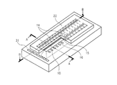
[インク吐出ヘッド]
図3は、本発明に係るインク吐出ヘッドの一例を示す斜視図である。図4は、図3のインク吐出ヘッドのA−A断面図である。
[Ink ejection head]
FIG. 3 is a perspective view showing an example of the ink ejection head according to the present invention. 4 is a cross-sectional view of the ink discharge head of FIG. 3 taken along the line AA.
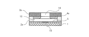
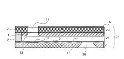
図4に示されるように、インク吐出ヘッド22は、基板1と、インク流路15を形成する流路形成部材21と、インク吐出口14を有する吐出口形成部材20とを備える。基板1はインク吐出エネルギー発生素子10を備え、インク供給口16が形成されている。吐出口形成部材20の表面には撥水膜6が設けられている。インク吐出口14は、開口の断面積が一定な部分と、該部分からインク吐出エネルギー発生素子10側に向けて開口の断面積が大きくなる部分とを有する。流路形成部材21により、インクを保持する液室13と、インク流路15とが形成されている。
As shown in FIG. 4, the
[インク吐出ヘッドの製造方法]
本発明に係るインク吐出ヘッドの製造方法は、基板と、該基板上に設けられるインク吐出エネルギー発生素子と、該基板上に設けられインク流路を形成する流路形成部材と、該インク吐出エネルギー発生素子と対向する位置にインク吐出口を有する吐出口形成部材と、を備えるインク吐出ヘッドの製造方法であって、
前記インク吐出口が、外部に開口する側に断面積が一定である部分と、該部分から前記インク吐出エネルギー発生素子側に向けて断面積が大きくなる部分とを有し、
基板上に流路形成部材となる第一のネガ型感光性レジストを形成する工程と、
前記第一のネガ型感光性レジスト上に吐出口形成部材となる第二のネガ型感光性レジストを形成する工程と、
前記第一のネガ型感光性レジストと前記第二のネガ型感光性レジストとを一部混合して相溶層を形成する工程と、
前記第二のネガ型感光性レジスト及び前記相溶層を一括露光し、現像することでインク吐出口を形成する工程と、を含む。
[Method of manufacturing ink discharge head]
An ink discharge head manufacturing method according to the present invention includes a substrate, an ink discharge energy generating element provided on the substrate, a flow path forming member provided on the substrate and forming an ink flow path, and the ink discharge energy. A method of manufacturing an ink ejection head comprising: an ejection port forming member having an ink ejection port at a position facing a generating element,
The ink discharge port has a portion having a constant cross-sectional area on the side that opens to the outside, and a portion having a cross-sectional area that increases from the portion toward the ink discharge energy generating element side,
Forming a first negative photosensitive resist serving as a flow path forming member on the substrate;
Forming a second negative photosensitive resist serving as a discharge port forming member on the first negative photosensitive resist;
A step of partially mixing the first negative photosensitive resist and the second negative photosensitive resist to form a compatible layer;
Forming the ink discharge port by collectively exposing and developing the second negative photosensitive resist and the compatible layer.
本発明に係る方法によれば、基板と密着する流路形成部材となる第一のネガ型感光性レジストに光吸収剤を添加する必要がなく、適切な露光量で第一のネガ型感光性レジストを露光できる。このため、ノズルを構成する流路形成部材と基板との密着性が高く、テーパ形状のインク吐出口を有する信頼性の高いインク吐出ヘッドを得ることができる。 According to the method of the present invention, there is no need to add a light absorber to the first negative photosensitive resist that becomes a flow path forming member in close contact with the substrate, and the first negative photosensitive property can be obtained with an appropriate exposure amount. The resist can be exposed. For this reason, it is possible to obtain a highly reliable ink discharge head having high adhesion between the flow path forming member constituting the nozzle and the substrate and having a tapered ink discharge port.
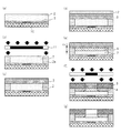
図1及び図2を用いて、本発明に係るインク吐出ヘッドの製造方法について説明する。図1及び図2は、図3に示されるインク吐出ヘッドのB−B断面図の一部(インク吐出口14の部分)である。なお、本発明に係る方法はこれらに限定されない。 A method for manufacturing an ink discharge head according to the present invention will be described with reference to FIGS. 1 and 2 are a part of the BB cross-sectional view of the ink discharge head shown in FIG. 3 (the portion of the ink discharge port 14). The method according to the present invention is not limited to these.
まず、図2(a)に示すように、インク吐出エネルギー発生素子10および保護層5が形成されたシリコンからなる基板1上に、第一のネガ型感光性レジスト2を形成する。インク吐出エネルギー発生素子10としては、電気熱変換素子、圧電素子等が挙げられる。保護層5の材料としては、SiO2等を用いることができる。第一のネガ型感光性レジスト2としては化学増幅型レジストを用いることができる。第一のネガ型感光性レジスト2に含まれる樹脂成分としては、エポキシ樹脂、シリコン系高分子化合物、α−位に水素原子を有するビニル系高分子化合物等を用いることができる。この中でも、該樹脂成分としてはエポキシ樹脂が好ましい。エポキシ樹脂としては、フェノールノボラック樹脂、クレゾールノボラック樹脂、エポキシ化ポリブタジエン等のエポキシ化ゴム等が挙げられる。これらは一種以上を用いてもよく、二種以上を併用してもよい。また、第一のネガ型感光性レジスト2は光酸発生剤を含むことができる。光酸発生剤としては、トリアリールスルホニウム塩、オニウム塩等を用いることができる。これらは一種以上を用いてもよく、二種以上を併用してもよい。さらに、第一のネガ型感光性レジスト2は溶媒を含むことができる。該溶媒としては、プロピレングリコールモノメチルエーテルアセテート(以下、PGMEAと示す)、γ−ブチロラクトン等を用いることができる。これらは一種以上を用いてもよく、二種以上を併用してもよい。該溶媒の沸点は、100℃以上、250℃以下であることが好ましい。なお、本発明における沸点は文献値である。また、該溶媒は、後述する第二のネガ型感光性レジスト3に含まれる溶媒、第二のネガ型感光性レジスト上に塗布される溶媒12と同一であってもよい。
First, as shown in FIG. 2A, a first negative photosensitive resist 2 is formed on a
第一のネガ型感光性レジスト2に含まれる樹脂成分の割合としては、例えば19.9質量%以上、70.0質量%以下とすることができる。第一のネガ型感光性レジスト2に含まれる光酸発生剤の割合としては、例えば0.1質量%以上、2.5質量%以下とすることができる。第一のネガ型感光性レジスト2に含まれる溶媒の割合としては、例えば29.9質量%以上、80.0質量%以下とすることができる。 The ratio of the resin component contained in the first negative photosensitive resist 2 can be, for example, 19.9 mass% or more and 70.0 mass% or less. As a ratio of the photo-acid generator contained in the 1st negative photosensitive resist 2, it can be 0.1 mass% or more and 2.5 mass% or less, for example. As a ratio of the solvent contained in the 1st negative photosensitive resist 2, it can be 29.9 mass% or more and 80.0 mass% or less, for example.
第一のネガ型感光性レジスト2の形成方法としては、ソルベントコート法、ドライフィルムを作製し基板上に転写する方法等が挙げられる。ソルベントコート法とは、レジスト溶液をスピンコーター、ロールコーター又はワイヤーバー等により基板上に塗布した後、溶媒を乾燥して除去し、レジスト層を形成する方法である。例えば、前記樹脂成分と、前記光酸発生剤と、前記溶媒とを含む溶液を基板1上にスピンコート法により塗布し、乾燥することにより、第一のネガ型感光性レジスト2を形成することができる。第一のネガ型感光性レジスト2の膜厚は特に限定されないが、例えば5μm以上、30μm以下とすることができる。
Examples of the method for forming the first negative photosensitive resist 2 include a solvent coating method and a method of producing a dry film and transferring it onto a substrate. The solvent coating method is a method of forming a resist layer by applying a resist solution on a substrate with a spin coater, a roll coater, a wire bar or the like and then drying and removing the solvent. For example, the first negative photosensitive resist 2 is formed by applying a solution containing the resin component, the photoacid generator, and the solvent onto the
第一のネガ型感光性レジスト2の溶解度パラメータ(SP値)は、5以上、13以下であることが好ましい。なお、本発明においてSP値は物性値から推算した値である。具体的には、溶解度パラメータδは、蒸発エンタルピーをΔH、モル体積をVとおくと、δ=√(ΔH−RT)/Vで定義されるため、各材料の物性値を文献から引用して推算できる。 The solubility parameter (SP value) of the first negative photosensitive resist 2 is preferably 5 or more and 13 or less. In the present invention, the SP value is a value estimated from a physical property value. Specifically, since the solubility parameter δ is defined as δ = √ (ΔH−RT) / V where the evaporation enthalpy is ΔH and the molar volume is V, the physical property values of each material are cited from the literature. Can be estimated.
次に、図2(b)に示すように、マスクを介して第一のネガ型感光性レジスト2を選択的に露光してインク流路パターンを潜像させ、その後露光後ベーク(以下、PEB(Post Exposure Bake)と示す)を行う。これにより、第一のネガ型感光性レジスト(硬化部)2aを形成する。露光には紫外線や電離放射線等を用いることができる。露光量は所望のパターンが形成できれば特に限定されないが、例えば3000J/m2以上、10000J/m2以下とすることができる。PEBの温度及び時間についても、所望のパターンが形成できれば特に限定されないが、例えば40℃以上、105℃以下で3分以上、15分以下行うことができる。 Next, as shown in FIG. 2B, the first negative photosensitive resist 2 is selectively exposed through a mask to form a latent image of the ink flow path pattern, and then post-exposure baking (hereinafter referred to as PEB). (Denoted as Post Exposure Bake). Thereby, the first negative photosensitive resist (cured portion) 2a is formed. For the exposure, ultraviolet rays, ionizing radiation, or the like can be used. Although the amount of exposure is not particularly limited as long as a desired pattern can be formed, for example, it can be 3000 J / m 2 or more and 10,000 J / m 2 or less. The temperature and time of PEB are not particularly limited as long as a desired pattern can be formed. For example, it can be performed at 40 ° C. or more and 105 ° C. or less for 3 minutes or more and 15 minutes or less.
次に、図2(c)に示すように、第一のネガ型感光性レジスト2上に、第二のネガ型感光性レジスト3を形成する。第二のネガ型感光性レジスト3としては化学増幅型レジストを用いることができる。第二のネガ型感光性レジスト3に含まれる樹脂成分としては、第一のネガ型感光性レジスト2に含まれる樹脂成分と同様のものを用いることができる。また、第二のネガ型感光性レジスト3は光酸発生剤を含むことができる。光酸発生剤としては、所望のパターンを形成できるものであれば特に限定されず、第一のネガ型感光性レジスト2に含まれる光酸発生剤と同様のものを用いることができる。さらに、第二のネガ型感光性レジスト3は溶媒を含むことができる。溶媒としては、PGMEA、γ−ブチロラクトン等を用いることができる。これらは一種以上を用いてもよく、二種以上を併用してもよい。該溶媒の沸点は、100℃以上、250℃以下であることが好ましい。なお、該溶媒は、第一のネガ型感光性レジスト2に含まれる溶媒、後述する第二のネガ型感光性レジスト3上に塗布される溶媒12と同一であってもよい。 Next, as shown in FIG. 2C, a second negative photosensitive resist 3 is formed on the first negative photosensitive resist 2. As the second negative photosensitive resist 3, a chemically amplified resist can be used. As the resin component contained in the second negative photosensitive resist 3, the same resin component as that contained in the first negative photosensitive resist 2 can be used. The second negative photosensitive resist 3 can contain a photoacid generator. The photoacid generator is not particularly limited as long as it can form a desired pattern, and the same photoacid generator as that contained in the first negative photosensitive resist 2 can be used. Furthermore, the second negative photosensitive resist 3 can contain a solvent. As the solvent, PGMEA, γ-butyrolactone, or the like can be used. These may use 1 or more types, and may use 2 or more types together. The boiling point of the solvent is preferably 100 ° C. or higher and 250 ° C. or lower. The solvent may be the same as the solvent contained in the first negative photosensitive resist 2 and the solvent 12 applied on the second negative photosensitive resist 3 described later.
第二のネガ型感光性レジスト3に含まれる樹脂成分の割合としては、例えば19.9質量%以上、70.0質量%以下とすることができる。第二のネガ型感光性レジスト3に含まれる光酸発生剤の割合としては、例えば0.1質量%以上、2.5質量%以下とすることができる。第二のネガ型感光性レジスト3に含まれる溶媒の割合としては、例えば29.9質量%以上、80.0質量%以下とすることができる。 As a ratio of the resin component contained in the 2nd negative photosensitive resist 3, it can be 19.9 mass% or more and 70.0 mass% or less, for example. As a ratio of the photo-acid generator contained in the 2nd negative photosensitive resist 3, it can be 0.1 mass% or more and 2.5 mass% or less, for example. As a ratio of the solvent contained in the 2nd negative photosensitive resist 3, it can be 29.9 mass% or more and 80.0 mass% or less, for example.
本発明においては、後述する相溶層4の感度を調整する観点から、第二のネガ型感光性レジスト3の露光に対する感度が、第一のネガ型感光性レジスト2の露光に対する感度よりも高いことが好ましい。すなわち、第二のネガ型感光性レジスト3の方が、第一のネガ型感光性レジスト2よりも光酸発生剤を多く含むことが好ましい。
In the present invention, from the viewpoint of adjusting the sensitivity of the
第二のネガ型感光性レジスト3の形成方法としては、ソルベントコート法、ドライフィルムを作製し基板上に転写する方法等が挙げられる。しかしながら、ソルベントコート法で塗布すると、第二のネガ型感光性レジスト3に含まれる溶媒が第一のネガ型感光性レジスト2を溶解してしまうなどの観点からドライフィルムを作製し基板上に転写する方法が好ましい。 Examples of the method for forming the second negative photosensitive resist 3 include a solvent coating method and a method of producing a dry film and transferring it onto a substrate. However, when applied by the solvent coating method, a dry film is produced and transferred onto the substrate from the viewpoint that the solvent contained in the second negative photosensitive resist 3 dissolves the first negative photosensitive resist 2. Is preferred.
第二のネガ型感光性レジスト3の膜厚は特に限定されないが、例えば3μm以上、60μm以下とすることができる。 Although the film thickness of the 2nd negative photosensitive resist 3 is not specifically limited, For example, it can be 3 micrometers or more and 60 micrometers or less.
次に、図2(d)に示すように、第二のネガ型感光性レジスト3上に溶媒12を塗布する。溶媒12としては、PGMEA、γ−ブチロラクトン、トルエン、α−テルピネオール、酢酸エチル、アセトン等が挙げられる。これらは一種のみを用いてもよく、二種以上を併用してもよい。溶媒12のSP値は、5以上、13以下であることが好ましい。なお、溶媒12は、第一のネガ型感光性レジスト2に含まれる溶媒、第二のネガ型感光性レジスト3に含まれる溶媒と同一であってもよい。 Next, as shown in FIG. 2D, a solvent 12 is applied on the second negative photosensitive resist 3. Examples of the solvent 12 include PGMEA, γ-butyrolactone, toluene, α-terpineol, ethyl acetate, acetone and the like. These may use only 1 type and may use 2 or more types together. The SP value of the solvent 12 is preferably 5 or more and 13 or less. The solvent 12 may be the same as the solvent contained in the first negative photosensitive resist 2 and the solvent contained in the second negative photosensitive resist 3.
第二のネガ型感光性レジスト3と、溶媒12とのSP値の差の絶対値は3.0以下であることが好ましい。該SP値の差の絶対値が3.0以下であることにより、溶媒12が第一のネガ型感光性レジスト2まで浸透し、第一のネガ型感光性レジスト2と第二のネガ型感光性レジスト3とが一部混合されて相溶層4が形成されやすい。該SP値の差の絶対値は2.5以下がより好ましく、2.0以下がさらに好ましい。また、第一のネガ型感光性レジスト2と溶媒12とのSP値の差の絶対値は3.0以下が好ましい。 The absolute value of the difference in SP value between the second negative photosensitive resist 3 and the solvent 12 is preferably 3.0 or less. When the absolute value of the difference between the SP values is 3.0 or less, the solvent 12 penetrates to the first negative photosensitive resist 2 and the first negative photosensitive resist 2 and the second negative photosensitive resist. The compatible resist 4 is easily formed by mixing a part of the compatible resist 3. The absolute value of the difference between the SP values is more preferably 2.5 or less, and further preferably 2.0 or less. The absolute value of the difference in SP value between the first negative photosensitive resist 2 and the solvent 12 is preferably 3.0 or less.
溶媒12の沸点は220℃以下であることが好ましい。溶媒12の沸点が220℃以下であることにより、溶媒12が第二のネガ型感光性レジスト3に浸透してから溶媒12が揮発するまでの時間を長くすることができる。このため、溶媒12を十分に第二のネガ型感光性レジスト3および第一のネガ型感光性レジスト2に浸透させることができ、相溶層4を形成することができる。溶媒12の沸点は50℃以上、200℃以下がより好ましく、70℃以上、150℃以下がさらに好ましい。
The boiling point of the solvent 12 is preferably 220 ° C. or lower. When the boiling point of the solvent 12 is 220 ° C. or less, it is possible to lengthen the time from when the solvent 12 penetrates the second negative photosensitive resist 3 until the solvent 12 volatilizes. Therefore, the solvent 12 can be sufficiently permeated into the second negative photosensitive resist 3 and the first negative photosensitive resist 2, and the
また、溶媒12の沸点は、第二のネガ型感光性レジスト3に含まれる溶媒の沸点以下であることが、相溶層4の膜厚制御の観点から好ましい。溶媒12の沸点は、第二のネガ型感光性レジスト3に含まれる溶媒の沸点より10℃以上低いことがより好ましく、30℃以上低いことがさらに好ましい。
Further, the boiling point of the solvent 12 is preferably not more than the boiling point of the solvent contained in the second negative photosensitive resist 3 from the viewpoint of controlling the film thickness of the
溶媒12の塗布方法は特に限定されないが、例えばスリットコーターによる塗布方法、スピンコートによる塗布方法等が挙げられる。 Although the coating method of the solvent 12 is not specifically limited, For example, the coating method by a slit coater, the coating method by spin coating, etc. are mentioned.
溶媒12のSP値、溶媒12の沸点、溶媒12の塗布量、溶媒12の塗布後から乾燥を行うまでの時間、および乾燥条件等によって相溶層4の膜厚が変化する。溶媒12の塗布量としては、1μm2あたり1.0×10⁻⁹ml以上、6.0×10⁻⁹ml以下とすることができる。溶媒12の塗布後から乾燥を行うまでの時間としては、15〜60秒とすることができる。溶媒12を乾燥する温度としては、40℃以上、90℃以下とすることができる。溶媒12を乾燥する時間としては、3分以上、15分以下とすることができる。
The film thickness of the
溶媒12が第二のネガ型感光性レジスト3および第一のネガ型感光性レジスト2に浸透することにより、図2(e)に示すように、第一のネガ型感光性レジスト2と第二のネガ型感光性レジスト3とが一部混合されて相溶層4が形成される。相溶層4の膜厚Cとしては、テーパ形状のインク吐出口を容易に形成できる観点から、0.5μm以上、30.0μm以下が好ましく、3.0μm以上、10.0μm以下がより好ましい。
When the solvent 12 permeates the second negative photosensitive resist 3 and the first negative photosensitive resist 2, as shown in FIG. 2 (e), the first negative photosensitive resist 2 and the second negative photosensitive resist 2 The negative photosensitive resist 3 is partially mixed to form the
溶媒12はそのまま第二のネガ型感光性レジスト3上に塗布してもよいが、溶媒12を含む第三の材料を塗布してもよい。第三の材料は撥水性を有することが好ましい。これにより、相溶層4を形成すると同時に、第二のネガ型感光性レジスト3上に撥水膜を形成することができる。また、該撥水膜の撥水性は、溶媒12を含まない第三の材料を塗布することで形成した撥水膜の撥水性と同等である。第三の材料に含まれる撥水剤としては、フッ素系の撥水剤、シリコン系の撥水剤等を用いることができる。これらは一種のみを用いてもよく、二種以上を併用してもよい。撥水膜の膜厚は、0.1μm以上、1.0μm以下であることが好ましい。
The solvent 12 may be applied as it is on the second negative photosensitive resist 3, but a third material containing the solvent 12 may be applied. The third material preferably has water repellency. Thereby, a water-repellent film can be formed on the second negative photosensitive resist 3 at the same time as forming the
第三の材料に含まれる溶媒12の割合は、5質量%以上、70質量以下であることが好ましい。該割合が5質量%以上であることにより、溶媒12が浸透して相溶層4が形成されやすい。また、該割合が70質量%以下であることにより、その形状を維持してテーパ形状のインク吐出口を形成することができる。該割合は20質量%以上、60質量%以下であることがより好ましく、30質量%以上、50質量%以下であることがさらに好ましい。
The ratio of the solvent 12 contained in the third material is preferably 5% by mass or more and 70% by mass or less. When the ratio is 5% by mass or more, the solvent 12 permeates and the
尚、相溶層4の形成方法は、溶媒12の浸透による方法に限られるものではない。例えば、熱によって相溶層4を形成することもできる。第二のネガ型感光性レジスト3を第一のネガ型感光性レジスト2上に形成する際に加熱する。加熱温度を、第一のネガ型感光性レジスト2及び第二のネガ型感光性レジスト3を十分に軟化させる温度とする。具体的には、レジストに一般的なエポキシ樹脂を用いた場合、該温度は、30℃以上であることが好ましく、50℃以上であることがより好ましい。また、該温度は180℃以下であることが好ましく、120℃以下であることがより好ましい。このように、第二のネガ型感光性レジスト3を第一のネガ型感光性レジスト2上に形成する際に加熱することで、第一のネガ型感光性レジスト2及び第二のネガ型感光性レジスト3を軟化させ、必要に応じて圧力を加えることによって2つのレジストが混合し、相溶層4が形成される。
In addition, the formation method of the
また、相溶層4の形成方法として、レジストに含有される残留溶媒を利用する方法も挙げられる。具体的には、図2(c)に示される工程において、第二のネガ型感光性レジスト3を転写する前の第一のネガ型感光性レジスト2及び第二のネガ型感光性レジスト3に含まれる残留溶媒量を、5質量%以上20質量%以下とすることが好ましい。ここでいう残留溶媒量とは、レジスト内に含まれる溶媒の、レジスト全体に対する質量%のことを意味する。残留溶媒量の調整は、例えば乾燥条件の調整によって行うことができる。このようにレジストに残留溶媒が十分に残った状態で転写を行うことで、溶媒を塗布しなくとも第一のネガ型感光性レジスト2及び第二のネガ型感光性レジスト3が混合し、相溶層4が形成される。
In addition, as a method for forming the
以上のようにして相溶層4を形成後、図2(f)に示すように、マスクを介して第二のネガ型感光性レジスト3及び相溶層4を選択的に一括露光してインク吐出口パターンを潜像させ、その後PEBを行う。溶媒12を含む第三の材料を塗布した場合には、第三の材料も一括露光する。露光条件及びPEB条件は、所望のインク吐出口パターンが形成できれば特に制限されるものではない。相溶層4が第二のネガ型感光性レジスト3よりも低い感度を有することで、適切な露光条件で露光を行うことにより、後の現像においてテーパ形状のインク吐出口が形成される。露光には、例えば紫外線や電離放射線等を用いることができる。露光量は、例えば400J/m2以上、2000J/m2以下とすることができる。PEBの温度及び時間については、例えば70℃以上、105℃以下で3分以上、10分以下行うことができる。
After forming the
次に、図2(g)に示すように、第一のネガ型感光性レジスト2、第二のネガ型感光性レジスト3及び相溶層4を一括現像してインク流路及びインク吐出口を形成する。溶媒12を含む第三の材料を塗布した場合には、第三の材料も一括現像する。現像はPGMEA(プロピレングリコールモノメチルエーテルアセテート)等を用いて行うことができる。これにより、外部に開口する側に断面積が一定である部分と、該部分から前記インク吐出エネルギー発生素子側に向けて断面積が大きくなる部分とを有するテーパ形状のインク吐出口が形成される。また、流路形成部材と基板との密着性も良好である。インク吐出口のテーパ角は3°以上、30°以下であることが好ましい。
Next, as shown in FIG. 2 (g), the first negative photosensitive resist 2, the second negative photosensitive resist 3, and the
次に、基板1にインク供給口を形成し、基板1をダイシングソー等により切断分離してチップ化する。その後、インク吐出エネルギー発生素子10を駆動させるための電気的接合を行う。さらに、インク供給のためのチップタンク部材を接続して、インク吐出ヘッドが完成する。
Next, an ink supply port is formed in the
本発明に係る方法では、第二のネガ型感光性レジスト3上に溶媒12を塗布することにより、溶媒12が第一のネガ型感光性レジスト2まで浸透し、二層間で相溶層4が形成される。また、熱により、又はレジストに含まれる残留溶媒により相溶層4を形成してもよい。この相溶層4が第二のネガ型感光性レジスト3よりも低感度であることを利用して、テーパ形状のインク吐出口を有する吐出口形成部材を、流路形成部材と基板1との密着性を低下させることなく形成することができる。
In the method according to the present invention, the solvent 12 penetrates to the first negative photosensitive resist 2 by applying the solvent 12 on the second negative photosensitive resist 3, and the
また、本発明に係る方法によって形成されるインク吐出ヘッドは、インク吐出時の前方抵抗が低減されるため、高い粘度のインクでも安定して吐出することができる。 In addition, the ink ejection head formed by the method according to the present invention reduces the forward resistance during ink ejection, and thus can stably eject even high viscosity ink.
[実施例1]
図2を用いて、実施例1に係るインク吐出ヘッドの製造方法を説明する。図2(a)〜(g)は本実施例に係るインク吐出ヘッドの製造方法を示す断面図である。
[Example 1]
A method for manufacturing the ink discharge head according to the first embodiment will be described with reference to FIG. 2A to 2G are cross-sectional views illustrating a method for manufacturing an ink discharge head according to the present embodiment.
まず、図2(a)に示すように、基板1上に第一のネガ型感光性レジスト2(以下、レジスト2と示す)を形成した。基板1にはシリコン基板を用いた。基板1には、電気熱変換素子であるインク吐出エネルギー発生素子10と、SiO2を含む保護層5とが設けられている。レジスト2は、エポキシ樹脂(商品名:SU−8、日本化薬製)からなる樹脂成分と、PGMEAからなる溶媒と、トリアリールスルホニウム塩からなる光酸発生剤と、アミン化合物からなる酸失活剤とを含む溶液をスピンコート法により塗布し、乾燥して形成した。レジスト2の膜厚は8μmであった。レジスト2に含まれる樹脂成分の割合は60質量%、光酸発生剤の割合は0.75質量%、酸失活剤の割合は0.25質量%、溶媒の割合は39質量%であった。即ち、レジスト2の残留溶媒量は39質量%である。また、レジスト2の軟化点は約70℃であった。
First, as shown in FIG. 2A, a first negative photosensitive resist 2 (hereinafter referred to as a resist 2) was formed on a
次に、図2(b)に示すように、マスク11を介してレジスト2に対してインク流路パターンを選択的に露光し、その後PEB(Post Exposure Bake)を行った。露光には紫外線を用いた。露光量は10000(J/m2)とした。PEBは60℃で10分間行った。 Next, as shown in FIG. 2B, the ink flow path pattern was selectively exposed to the resist 2 through the mask 11, and then PEB (Post Exposure Bake) was performed. Ultraviolet rays were used for exposure. The exposure amount was 10,000 (J / m 2 ). PEB was performed at 60 ° C. for 10 minutes.
次に、図2(c)に示すように、レジスト2上に第二のネガ型感光性レジスト3(以下レジスト3と示す)を形成した。レジスト3は、エポキシ樹脂(前記レジスト2と同じ)からなる樹脂成分と、PGMEAからなる溶媒と、トリアリールスルホニウム塩からなる光酸発生剤とを含むレジストをドライフィルムとしたものである。ドライフィルムにする前のレジストに含まれる樹脂成分の割合は50質量%、溶媒の割合は49質量%、光酸発生剤の割合は1質量%であった。このレジストを乾燥させてドライフィルムとした。レジスト3の溶媒量、即ち残留溶媒量は0.1質量%であった。また、レジスト3の軟化点は約70℃であった。レジスト3はラミネートによるドライフィルム転写により形成した。転写温度は55℃、転写時間は1分とした。レジスト3の膜厚は8μmであった。なお、本実施例ではレジスト2を低感度とし、レジスト3を高感度として相溶層の感度を調整するため、レジスト3の感度をレジスト2の感度よりも高くした。すなわち、レジスト2よりもレジスト3の方が光酸発生剤を多量に含むようにした。また、レジスト3のSP値は9.7〜10.9であった。 Next, as shown in FIG. 2C, a second negative photosensitive resist 3 (hereinafter referred to as a resist 3) was formed on the resist 2. The resist 3 is a dry film made of a resist containing a resin component made of an epoxy resin (same as the resist 2), a solvent made of PGMEA, and a photoacid generator made of a triarylsulfonium salt. The ratio of the resin component contained in the resist before forming a dry film was 50 mass%, the ratio of the solvent was 49 mass%, and the ratio of the photoacid generator was 1 mass%. This resist was dried to obtain a dry film. The solvent amount of the resist 3, that is, the residual solvent amount was 0.1% by mass. The softening point of the resist 3 was about 70 ° C. The resist 3 was formed by dry film transfer by lamination. The transfer temperature was 55 ° C. and the transfer time was 1 minute. The film thickness of the resist 3 was 8 μm. In this example, the sensitivity of the resist 3 is set higher than that of the resist 2 in order to adjust the sensitivity of the compatible layer by setting the resist 2 to be low sensitivity and the resist 3 to be high sensitivity. That is, the resist 3 contains a larger amount of photoacid generator than the resist 2. The SP value of resist 3 was 9.7 to 10.9.
次に、図2(d)に示すように、レジスト3上に溶媒12を塗布した。溶媒12としてはPGMEAを用いた。溶媒12をスリットコーターにより塗布した。溶媒12の塗布条件としては、1μm2あたり3.0×10⁻⁹mlの溶媒12を塗布した。溶媒12の塗布後から乾燥を行うまでの時間は40秒であった。溶媒12の乾燥は、60℃で10分間行った。
Next, as shown in FIG. 2D, a solvent 12 was applied on the resist 3. PGMEA was used as the solvent 12.
レジスト3と溶媒12とのSP値の差の絶対値は3.0以下であるため、溶媒12はレジスト3に十分に浸透した。その結果、図2(e)に示す膜厚Cが3μmである相溶層4が形成された。
Since the absolute value of the difference in SP value between the resist 3 and the solvent 12 is 3.0 or less, the solvent 12 has sufficiently penetrated into the resist 3. As a result, a
次に、図2(f)に示すように、マスクを介してレジスト3及び相溶層4に対して吐出口パターンを選択的に一括露光し、その後PEBを行った。露光には紫外線を用いた。露光量は1000(J/m2)とした。PEBは105℃で10分間行った。
Next, as shown in FIG. 2F, the discharge port pattern was selectively collectively exposed to the resist 3 and the
次に、図2(g)に示すように、レジスト2、レジスト3及び相溶層4を一括現像した。現像はPGMEAを用いて行った。これにより、外部に開口する側に断面積が一定である部分と、該部分から前記インク吐出エネルギー発生素子側に向けて断面積が大きくなる部分とを有するインク吐出口が形成された。インク吐出口のテーパ角は15°であった。
Next, as shown in FIG. 2G, the resist 2, the resist 3, and the
次に、基板1にインク供給口を形成後、基板1をダイシングソーにより切断分離してチップ化し、インク吐出エネルギー発生素子10を駆動させるための電気的接合を行った。その後、インク供給のためのチップタンク部材を接続して、インク吐出ヘッドを完成させた。
Next, after an ink supply port was formed in the
[実施例2]
溶媒12として、PGMEAを用いる代わりにアセトンを用いた以外は実施例1と同様にインク吐出ヘッドを製造した。相溶層4の膜厚Cは2.2μmであり、テーパ角が10°のテーパ形状のインク吐出口が形成された。
[Example 2]
An ink discharge head was manufactured in the same manner as in Example 1 except that acetone was used as the solvent 12 instead of PGMEA. The thickness C of the
なお、アセトンのSP値は10.0であり、SP値が8.7のPGMEAよりも溶解性が高い。一方、アセトンの沸点は56.5℃と低く、飽和蒸気圧も20℃で24.7kPaと高い。このため、アセトンは、沸点が146℃、飽和蒸気圧が20℃で3.8kPaのPGMEAと比較して、低温でも揮発しやすい。アセトンは溶解性が高いものの、レジスト3に浸透してから揮発するまでの時間が短いため、十分に浸透する前に揮発してしまい、相溶層4の膜厚CはPGMEAを用いた実施例1と比較して薄くなった。
In addition, SP value of acetone is 10.0, and its solubility is higher than PGMEA with SP value of 8.7. On the other hand, the boiling point of acetone is as low as 56.5 ° C., and the saturated vapor pressure is as high as 24.7 kPa at 20 ° C. For this reason, acetone has a boiling point of 146 ° C., a saturated vapor pressure of 20 ° C., and volatilizes easily even at a low temperature compared to 3.8 kPa PGMEA. Although acetone has a high solubility, it has a short time until it volatilizes after penetrating into the resist 3, and therefore volatilizes before sufficiently penetrating. The film thickness C of the
[実施例3]
実施例1と同様に、図2(a)〜(c)に示される工程を行った。
[Example 3]
Similar to Example 1, the steps shown in FIGS. 2A to 2C were performed.
次に、レジスト3上に溶媒を含む第三の材料を塗布した。第三の材料にはフッ素系の撥水剤を用いた。溶媒としてはPGMEAを用いた。第三の材料に含まれる溶媒の割合は50質量%とした。第三の材料をスリットコーターにより塗布した。第三の材料の塗布量は、形成される撥水膜6の膜厚が1μm未満になる塗布量とした。第三の材料の塗布後から乾燥を行うまでの時間は40秒であった。溶媒12の乾燥は、60℃で10分間行った。形成された撥水膜6の膜厚は0.8μmであった。 Next, a third material containing a solvent was applied onto the resist 3. A fluorine-based water repellent was used as the third material. PGMEA was used as the solvent. The ratio of the solvent contained in the third material was 50% by mass. The third material was applied with a slit coater. The application amount of the third material was such that the film thickness of the formed water repellent film 6 was less than 1 μm. The time from application of the third material to drying was 40 seconds. The solvent 12 was dried at 60 ° C. for 10 minutes. The formed water repellent film 6 had a thickness of 0.8 μm.
その後は実施例1と同様に行い、インク吐出ヘッドを製造した。相溶層4の膜厚Cは3μmであり、テーパ角が15°のテーパ形状のインク吐出口が形成された。
Thereafter, the same procedure as in Example 1 was performed to manufacture an ink discharge head. The thickness C of the
溶媒を添加せずに撥水剤を塗布した場合と比較しても、撥水膜6の撥水性は低下しなかった。また、膜厚Cが3μmである相溶層4が得られた。このように、溶媒12を第三の材料に添加しても、撥水膜6の撥水性を低下させることなく相溶層4を形成できることがわかった。
The water repellency of the water repellent film 6 did not decrease even when compared with the case where a water repellent was applied without adding a solvent. Moreover, the
[実施例4]
実施例1と同様に、図2(a)〜(c)に示される工程を行った。
[Example 4]
Similar to Example 1, the steps shown in FIGS. 2A to 2C were performed.
次に、レジスト3上に溶媒を含む第三の材料を塗布した。第三の材料には、溶媒としてPGMEAが含まれる他に、固形分としてエポキシ樹脂(レジスト3に含まれる樹脂と同じ樹脂)と、光酸発生剤(トリアリールスルホニウム塩)が含まれる。第三の材料に含まれる溶媒の割合は50質量%とした。第三の材料をスリットコーターにより塗布した。第三の材料の塗布量は、形成される膜厚が1μm未満になる塗布量とした。第三の材料の塗布後から乾燥を行うまでの時間は40秒であった。第三の材料の乾燥は、60℃で10分間行った。形成された膜厚は1.0μmであった。 Next, a third material containing a solvent was applied onto the resist 3. In addition to containing PGMEA as a solvent, the third material contains an epoxy resin (the same resin as that contained in the resist 3) and a photoacid generator (triarylsulfonium salt) as a solid content. The ratio of the solvent contained in the third material was 50% by mass. The third material was applied with a slit coater. The coating amount of the third material was set to a coating amount at which the formed film thickness was less than 1 μm. The time from application of the third material to drying was 40 seconds. The third material was dried at 60 ° C. for 10 minutes. The formed film thickness was 1.0 μm.
その後は実施例1と同様に行い、インク吐出ヘッドを製造した。相溶層4の膜厚Cは3μmであり、テーパ角が15°のテーパ形状のインク吐出口が形成された。
Thereafter, the same procedure as in Example 1 was performed to manufacture an ink discharge head. The thickness C of the
本実施例では上記に加えて、第三の材料とレジスト3との間にも相溶層が形成されるため、吐出口形成部材および流路形成部材によって形成される吐出口パターンや、応力緩和パターンおよびノズル部端部のノズル表面側の角部を丸めることができる。角部を丸めることによって、ワイピング機構が駆動した時に角部がワイピング機構と接触することを防ぐことができるため、ノズルの信頼性を向上させることができる。 In this embodiment, in addition to the above, a compatible layer is also formed between the third material and the resist 3, so that the discharge port pattern formed by the discharge port forming member and the flow path forming member, and stress relaxation The corners on the nozzle surface side of the pattern and the nozzle end can be rounded. By rounding the corner portion, it is possible to prevent the corner portion from coming into contact with the wiping mechanism when the wiping mechanism is driven, so that the reliability of the nozzle can be improved.
このように、溶媒に樹脂と光酸発生剤を添加することによって、相溶層4を形成するとともに、角部を丸めてワイピング機構との接触を防止することのできる、信頼性の高いノズルを形成することができた。
Thus, by adding a resin and a photoacid generator to the solvent, a highly reliable nozzle that can form the
[実施例5]
実施例1と同様に、図2(a)〜(b)に示される工程を行った。
[Example 5]
Similar to Example 1, the steps shown in FIGS. 2A to 2B were performed.
次に、図2(c)に示すように、レジスト2上にレジスト3を形成した。レジスト3としては、実施例1と同じ材料を用いた。レジスト3はラミネートによるドライフィルム転写により形成したが、転写温度を85℃とした。転写時間は実施例1と同様に1分とした。 Next, a resist 3 was formed on the resist 2 as shown in FIG. As the resist 3, the same material as in Example 1 was used. The resist 3 was formed by dry film transfer by lamination, but the transfer temperature was 85 ° C. The transfer time was 1 minute as in Example 1.
本実施例においては、図2(d)の溶媒12の塗布工程は行わなかったが、図2(e)に示す膜厚Cが3μmである相溶層4が形成された。その後は実施例1と同様にして、インク吐出ヘッドを完成させた。得られたインクジェット記録ヘッドは、外部に開口する側に断面積が一定である部分と、該部分から前記インク吐出エネルギー発生素子側に向けて断面積が大きくなる部分とを有するインク吐出口を有するものであった。また、インク吐出口のテーパ角は15°であった。
In this example, the solvent 12 application step of FIG. 2D was not performed, but a
[実施例6]
本実施例では、レジスト2の残留溶媒量を6.0質量%、レジスト3の残留溶媒量を8.0質量%とした。また、溶媒12の塗布工程は行わなかった。これ以外は、実施例1と同様にしてインク吐出ヘッドを完成させた。本実施例においては、図2(e)に示す膜厚Cが1μmである相溶層4が形成された。得られたインクジェット記録ヘッドは、外部に開口する側に断面積が一定である部分と、該部分から前記インク吐出エネルギー発生素子側に向けて断面積が大きくなる部分とを有するインク吐出口を有するものであった。また、インク吐出口のテーパ角は3°であった。
[Example 6]
In this example, the residual solvent amount of the resist 2 was 6.0 mass%, and the residual solvent amount of the resist 3 was 8.0 mass%. Moreover, the application | coating process of the solvent 12 was not performed. Except for this, an ink ejection head was completed in the same manner as in Example 1. In this example, a
[比較例1]
レジスト3としてSP値が9.6であるエポキシ樹脂を含有するドライフィルムレジストを用いた。また、溶媒12としてSP値が12.7であるエタノールを用いた。これら以外は実施例1と同様にインク吐出ヘッドを製造した。本比較例では溶媒12がレジスト3に浸透しなかったため、相溶層4は形成されなかった。
[Comparative Example 1]
A dry film resist containing an epoxy resin having an SP value of 9.6 was used as the resist 3. Further, ethanol having an SP value of 12.7 was used as the solvent 12. Other than these, an ink ejection head was manufactured in the same manner as in Example 1. In this comparative example, the solvent 12 did not penetrate into the resist 3, so the
[比較例2]
第三の材料に含まれる溶媒の割合を3質量%とした以外は実施例3と同様にインク吐出ヘッドを製造した。本比較例では第三の材料に含まれる溶媒の割合が低いため、相溶層4は形成されなかった。
[Comparative Example 2]
An ink ejection head was manufactured in the same manner as in Example 3 except that the ratio of the solvent contained in the third material was 3% by mass. In this comparative example, since the ratio of the solvent contained in the third material was low, the
[実施例7]
第三の材料に含まれる溶媒の割合を5質量%とした以外は実施例3と同様にインク吐出ヘッドを製造した。本実施例では、膜厚Cが0.5μmの相溶層4が形成され、テーパ角が3°のテーパ形状のインク吐出口を形成することができた。
[Example 7]
An ink ejection head was manufactured in the same manner as in Example 3 except that the ratio of the solvent contained in the third material was changed to 5% by mass. In this example, the
[実施例8]
第三の材料に含まれる溶媒の割合を70質量%とした以外は実施例3と同様にインク吐出ヘッドを製造した。本実施例では、膜厚Cが4.0μmの相溶層4が形成され、テーパ角が20°のテーパ形状のインク吐出口を形成することができた。
[Example 8]
An ink discharge head was manufactured in the same manner as in Example 3 except that the ratio of the solvent contained in the third material was 70% by mass. In this example, the
[比較例3]
第三の材料に含まれる溶媒の割合を75質量%とした以外は実施例3と同様にインク吐出ヘッドを製造した。本比較例では第三の材料に含まれる溶媒の割合が高いため、インク吐出口の形状が崩れ、テーパ形状のインク吐出口を形成することができなかった。
[Comparative Example 3]
An ink ejection head was manufactured in the same manner as in Example 3 except that the ratio of the solvent contained in the third material was 75% by mass. In this comparative example, since the ratio of the solvent contained in the third material is high, the shape of the ink ejection port collapses and a tapered ink ejection port cannot be formed.
1 基板
2 第一のネガ型感光性レジスト
2a 第一のネガ型感光性レジスト(硬化部)
3 第二のネガ型感光性レジスト
3a 第二のネガ型感光性レジスト(硬化部)
4 相溶層
4a 相溶層(硬化部)
5 保護層
6 撥水膜
10 インク吐出エネルギー発生素子
11 マスク
12 溶媒
13 液室
14 インク吐出口
15 インク流路
16 インク供給口
20 吐出口形成部材
21 流路形成部材
22 インク吐出ヘッド
1
3 Second negative photosensitive resist 3a Second negative photosensitive resist (cured portion)
4
5 Protective layer 6
Claims (10)
前記インク吐出口が、外部に開口する側に断面積が一定である部分と、該部分から前記インク吐出エネルギー発生素子側に向けて断面積が大きくなる部分とを有し、
基板上に流路形成部材となる第一のネガ型感光性レジストを形成する工程と、
前記第一のネガ型感光性レジスト上に吐出口形成部材となる第二のネガ型感光性レジストを形成する工程と、
前記第二のネガ型感光性レジスト上に溶媒を含む第三の材料を塗布することで、前記第一のネガ型感光性レジストと前記第二のネガ型感光性レジストとを一部混合して相溶層を形成する工程と、
前記第二のネガ型感光性レジスト、前記第三の材料及び前記相溶層を一括露光し、現像することでインク吐出口を形成する工程と、を含むインク吐出ヘッドの製造方法。 A substrate, an ink discharge energy generating element provided on the substrate, a flow path forming member provided on the substrate to form an ink flow path, and an ink discharge port at a position facing the ink discharge energy generating element; A discharge port forming member, and a method of manufacturing an ink discharge head comprising:
The ink discharge port has a portion having a constant cross-sectional area on the side that opens to the outside, and a portion having a cross-sectional area that increases from the portion toward the ink discharge energy generating element side,
Forming a first negative photosensitive resist serving as a flow path forming member on the substrate;
Forming a second negative photosensitive resist serving as a discharge port forming member on the first negative photosensitive resist;
A part of the first negative photosensitive resist and the second negative photosensitive resist are mixed by applying a third material containing a solvent on the second negative photosensitive resist. Forming a compatible layer;
Forming the ink discharge port by collectively exposing and developing the second negative photosensitive resist , the third material, and the compatible layer, and a method of manufacturing the ink discharge head.
前記インク吐出口が、外部に開口する側に断面積が一定である部分と、該部分から前記インク吐出エネルギー発生素子側に向けて断面積が大きくなる部分とを有し、The ink discharge port has a portion having a constant cross-sectional area on the side that opens to the outside, and a portion having a cross-sectional area that increases from the portion toward the ink discharge energy generating element side,
基板上に流路形成部材となる第一のネガ型感光性レジストを形成する工程と、Forming a first negative photosensitive resist serving as a flow path forming member on the substrate;
前記第一のネガ型感光性レジスト上に吐出口形成部材となる第二のネガ型感光性レジストを形成する工程と、Forming a second negative photosensitive resist serving as a discharge port forming member on the first negative photosensitive resist;
前記第二のネガ型感光性レジスト上に溶媒を塗布することで、前記第一のネガ型感光性レジストと前記第二のネガ型感光性レジストとを一部混合して相溶層を形成する工程と、By applying a solvent on the second negative photosensitive resist, a part of the first negative photosensitive resist and the second negative photosensitive resist are mixed to form a compatible layer. Process,
前記第二のネガ型感光性レジスト及び前記相溶層を一括露光し、現像することでインク吐出口を形成する工程と、を含むインク吐出ヘッドの製造方法。Forming the ink discharge port by collectively exposing and developing the second negative photosensitive resist and the compatible layer, and a method for manufacturing the ink discharge head.
前記インク吐出口が、外部に開口する側に断面積が一定である部分と、該部分から前記インク吐出エネルギー発生素子側に向けて断面積が大きくなる部分とを有し、The ink discharge port has a portion having a constant cross-sectional area on the side that opens to the outside, and a portion having a cross-sectional area that increases from the portion toward the ink discharge energy generating element side,
基板上に流路形成部材となる第一のネガ型感光性レジストを形成する工程と、Forming a first negative photosensitive resist serving as a flow path forming member on the substrate;
前記第一のネガ型感光性レジスト上に吐出口形成部材となる第二のネガ型感光性レジストを加熱しながら塗布または転写することで、前記第一のネガ型感光性レジストと前記第二のネガ型感光性レジストとを一部混合して相溶層を形成しながら、前記第一のネガ型感光性レジスト上に前記第二のネガ型感光性レジストを形成する工程と、By applying or transferring a second negative photosensitive resist serving as a discharge port forming member on the first negative photosensitive resist while heating, the first negative photosensitive resist and the second negative photosensitive resist are applied. Forming the second negative photosensitive resist on the first negative photosensitive resist while forming a compatible layer by partially mixing the negative photosensitive resist;
前記第二のネガ型感光性レジスト及び前記相溶層を一括露光し、現像することでインク吐出口を形成する工程と、を含むインク吐出ヘッドの製造方法。Forming the ink discharge port by collectively exposing and developing the second negative photosensitive resist and the compatible layer, and a method for manufacturing the ink discharge head.
Priority Applications (1)
| Application Number | Priority Date | Filing Date | Title |
|---|---|---|---|
| JP2013235975A JP6242174B2 (en) | 2012-11-21 | 2013-11-14 | Manufacturing method of ink discharge head |
Applications Claiming Priority (3)
| Application Number | Priority Date | Filing Date | Title |
|---|---|---|---|
| JP2012255201 | 2012-11-21 | ||
| JP2012255201 | 2012-11-21 | ||
| JP2013235975A JP6242174B2 (en) | 2012-11-21 | 2013-11-14 | Manufacturing method of ink discharge head |
Publications (3)
| Publication Number | Publication Date |
|---|---|
| JP2014121873A JP2014121873A (en) | 2014-07-03 |
| JP2014121873A5 JP2014121873A5 (en) | 2016-12-08 |
| JP6242174B2 true JP6242174B2 (en) | 2017-12-06 |
Family
ID=50728268
Family Applications (1)
| Application Number | Title | Priority Date | Filing Date |
|---|---|---|---|
| JP2013235975A Expired - Fee Related JP6242174B2 (en) | 2012-11-21 | 2013-11-14 | Manufacturing method of ink discharge head |
Country Status (2)
| Country | Link |
|---|---|
| US (1) | US8778599B2 (en) |
| JP (1) | JP6242174B2 (en) |
Families Citing this family (4)
| Publication number | Priority date | Publication date | Assignee | Title |
|---|---|---|---|---|
| JP6308751B2 (en) | 2013-11-12 | 2018-04-11 | キヤノン株式会社 | Method for manufacturing substrate for liquid discharge head, substrate for liquid discharge head, liquid discharge head, and recording apparatus |
| JP6418023B2 (en) | 2015-03-24 | 2018-11-07 | ブラザー工業株式会社 | Method for manufacturing liquid ejection device |
| JP6746329B2 (en) * | 2016-03-11 | 2020-08-26 | キヤノン株式会社 | Method of manufacturing recording element substrate and liquid ejection head |
| JP7013274B2 (en) * | 2018-02-22 | 2022-01-31 | キヤノン株式会社 | Manufacturing method of liquid discharge head |
Family Cites Families (10)
| Publication number | Priority date | Publication date | Assignee | Title |
|---|---|---|---|---|
| JP2694054B2 (en) * | 1990-12-19 | 1997-12-24 | キヤノン株式会社 | Liquid jet recording head, method of manufacturing the same, and recording apparatus having liquid jet recording head |
| US6162589A (en) * | 1998-03-02 | 2000-12-19 | Hewlett-Packard Company | Direct imaging polymer fluid jet orifice |
| JP2004192011A (en) * | 1997-11-14 | 2004-07-08 | Fuji Photo Film Co Ltd | Photosensitive image forming material for infrared laser |
| US6709805B1 (en) * | 2003-04-24 | 2004-03-23 | Lexmark International, Inc. | Inkjet printhead nozzle plate |
| KR100657334B1 (en) * | 2005-09-13 | 2006-12-14 | 삼성전자주식회사 | Method for manufacturing inkjet printhead and inkjet printhead manufactured by the same |
| JP2007320299A (en) | 2006-06-05 | 2007-12-13 | Ricoh Co Ltd | Method for manufacturing droplet ejection head, droplet ejection head, liquid cartridge, droplet ejection apparatus, and line type droplet ejection apparatus |
| JP2008030272A (en) * | 2006-07-27 | 2008-02-14 | Canon Inc | Inkjet recording head, and its manufacturing method |
| US8109608B2 (en) * | 2007-10-04 | 2012-02-07 | Lexmark International, Inc. | Micro-fluid ejection head and stress relieved orifice plate therefor |
| JP5506600B2 (en) * | 2010-08-25 | 2014-05-28 | キヤノン株式会社 | Method for manufacturing liquid discharge head |
| JP6008598B2 (en) | 2012-06-11 | 2016-10-19 | キヤノン株式会社 | Discharge port forming member and liquid discharge head manufacturing method |
-
2013
- 2013-10-30 US US14/067,012 patent/US8778599B2/en not_active Expired - Fee Related
- 2013-11-14 JP JP2013235975A patent/JP6242174B2/en not_active Expired - Fee Related
Also Published As
| Publication number | Publication date |
|---|---|
| US20140141379A1 (en) | 2014-05-22 |
| JP2014121873A (en) | 2014-07-03 |
| US8778599B2 (en) | 2014-07-15 |
Similar Documents
| Publication | Publication Date | Title |
|---|---|---|
| JP3833989B2 (en) | Inkjet printhead manufacturing method | |
| US7226149B2 (en) | Plurality of barrier layers | |
| US9216570B2 (en) | Process for producing liquid ejection head | |
| JP2005205916A (en) | Method of manufacturing monolithic inkjet printhead | |
| JP6242174B2 (en) | Manufacturing method of ink discharge head | |
| KR20080102903A (en) | Method for manufacturing inkjet printhead and inkjet printhead manufactured by the same | |
| US8753800B2 (en) | Process for producing ejection orifice forming member and liquid ejection head | |
| EP1680278B1 (en) | Plurality of barrier layers | |
| JP2004090636A (en) | Ink-jet print head and manufacturing method therefor | |
| US7278709B2 (en) | Photo-curable resin composition, method of patterning the same, and ink jet head and method of fabricating the same | |
| US20100128091A1 (en) | Inkjet printhead and method of manufacturing the same | |
| JP6039259B2 (en) | Liquid discharge head and manufacturing method thereof | |
| JP2020062809A (en) | Manufacturing method of liquid discharge head | |
| KR20090030111A (en) | Method for manufacturing inkjet printhead and inkjet printhead manufactured by the same | |
| JP2003251808A (en) | Channel constituting member of inkjet recording head and manufacturing method for inkjet recording head | |
| JP5328606B2 (en) | Method for manufacturing liquid discharge head | |
| JP6388385B2 (en) | Liquid discharge head and method of manufacturing liquid discharge head | |
| US20120267342A1 (en) | Method of producing substrate for liquid ejection head | |
| JP2009172871A (en) | Manufacturing method of liquid discharge head | |
| US10632754B2 (en) | Perforated substrate processing method and liquid ejection head manufacturing method | |
| KR20090077233A (en) | Method for manufacturing inkjet printhead and inkjet printhead manufactured by the same | |
| US10500861B2 (en) | Method for manufacturing liquid ejection head | |
| US10442201B2 (en) | Method for manufacturing liquid ejection head | |
| US20130244183A1 (en) | Process for producing ink jet recording head | |
| JP2006082331A (en) | Process for manufacturing ink jet recording head |
Legal Events
| Date | Code | Title | Description |
|---|---|---|---|
| RD04 | Notification of resignation of power of attorney |
Free format text: JAPANESE INTERMEDIATE CODE: A7424 Effective date: 20140430 |
|
| A521 | Request for written amendment filed |
Free format text: JAPANESE INTERMEDIATE CODE: A523 Effective date: 20161020 |
|
| A621 | Written request for application examination |
Free format text: JAPANESE INTERMEDIATE CODE: A621 Effective date: 20161020 |
|
| A977 | Report on retrieval |
Free format text: JAPANESE INTERMEDIATE CODE: A971007 Effective date: 20170721 |
|
| A131 | Notification of reasons for refusal |
Free format text: JAPANESE INTERMEDIATE CODE: A131 Effective date: 20170801 |
|
| A521 | Request for written amendment filed |
Free format text: JAPANESE INTERMEDIATE CODE: A523 Effective date: 20171002 |
|
| TRDD | Decision of grant or rejection written | ||
| A01 | Written decision to grant a patent or to grant a registration (utility model) |
Free format text: JAPANESE INTERMEDIATE CODE: A01 Effective date: 20171010 |
|
| A61 | First payment of annual fees (during grant procedure) |
Free format text: JAPANESE INTERMEDIATE CODE: A61 Effective date: 20171107 |
|
| R151 | Written notification of patent or utility model registration |
Ref document number: 6242174 Country of ref document: JP Free format text: JAPANESE INTERMEDIATE CODE: R151 |
|
| LAPS | Cancellation because of no payment of annual fees |