US8080774B1 - Module for scalable millimeter wave imaging arrays - Google Patents
Module for scalable millimeter wave imaging arrays Download PDFInfo
- Publication number
- US8080774B1 US8080774B1 US12/190,453 US19045308A US8080774B1 US 8080774 B1 US8080774 B1 US 8080774B1 US 19045308 A US19045308 A US 19045308A US 8080774 B1 US8080774 B1 US 8080774B1
- Authority
- US
- United States
- Prior art keywords
- horn antenna
- detector
- millimeter wave
- module
- video output
- Prior art date
- Legal status (The legal status is an assumption and is not a legal conclusion. Google has not performed a legal analysis and makes no representation as to the accuracy of the status listed.)
- Expired - Fee Related, expires
Links
- 238000003384 imaging method Methods 0.000 title description 22
- 238000003491 array Methods 0.000 title description 10
- 239000000758 substrate Substances 0.000 claims description 39
- 238000000034 method Methods 0.000 claims description 17
- 230000007704 transition Effects 0.000 claims description 12
- 239000000523 sample Substances 0.000 claims description 9
- 238000004519 manufacturing process Methods 0.000 claims description 4
- 238000012986 modification Methods 0.000 description 4
- 230000004048 modification Effects 0.000 description 4
- 238000013461 design Methods 0.000 description 3
- 239000002184 metal Substances 0.000 description 3
- 239000010409 thin film Substances 0.000 description 2
- 241000408659 Darpa Species 0.000 description 1
- 239000004593 Epoxy Substances 0.000 description 1
- 239000004809 Teflon Substances 0.000 description 1
- 229920006362 Teflon® Polymers 0.000 description 1
- 230000006978 adaptation Effects 0.000 description 1
- PNEYBMLMFCGWSK-UHFFFAOYSA-N aluminium oxide Inorganic materials [O-2].[O-2].[O-2].[Al+3].[Al+3] PNEYBMLMFCGWSK-UHFFFAOYSA-N 0.000 description 1
- 230000003321 amplification Effects 0.000 description 1
- 239000004020 conductor Substances 0.000 description 1
- 230000008878 coupling Effects 0.000 description 1
- 238000010168 coupling process Methods 0.000 description 1
- 238000005859 coupling reaction Methods 0.000 description 1
- 238000001514 detection method Methods 0.000 description 1
- 238000011161 development Methods 0.000 description 1
- 238000004070 electrodeposition Methods 0.000 description 1
- 238000001746 injection moulding Methods 0.000 description 1
- 239000000463 material Substances 0.000 description 1
- 238000003199 nucleic acid amplification method Methods 0.000 description 1
- 230000008569 process Effects 0.000 description 1
- 239000010453 quartz Substances 0.000 description 1
- 238000011160 research Methods 0.000 description 1
- VYPSYNLAJGMNEJ-UHFFFAOYSA-N silicon dioxide Inorganic materials O=[Si]=O VYPSYNLAJGMNEJ-UHFFFAOYSA-N 0.000 description 1
- 229910000679 solder Inorganic materials 0.000 description 1
Images


Classifications
-
- G—PHYSICS
- G01—MEASURING; TESTING
- G01S—RADIO DIRECTION-FINDING; RADIO NAVIGATION; DETERMINING DISTANCE OR VELOCITY BY USE OF RADIO WAVES; LOCATING OR PRESENCE-DETECTING BY USE OF THE REFLECTION OR RERADIATION OF RADIO WAVES; ANALOGOUS ARRANGEMENTS USING OTHER WAVES
- G01S7/00—Details of systems according to groups G01S13/00, G01S15/00, G01S17/00
- G01S7/02—Details of systems according to groups G01S13/00, G01S15/00, G01S17/00 of systems according to group G01S13/00
- G01S7/03—Details of HF subsystems specially adapted therefor, e.g. common to transmitter and receiver
- G01S7/032—Constructional details for solid-state radar subsystems
-
- H—ELECTRICITY
- H01—ELECTRIC ELEMENTS
- H01Q—ANTENNAS, i.e. RADIO AERIALS
- H01Q13/00—Waveguide horns or mouths; Slot antennas; Leaky-waveguide antennas; Equivalent structures causing radiation along the transmission path of a guided wave
- H01Q13/02—Waveguide horns
-
- H—ELECTRICITY
- H01—ELECTRIC ELEMENTS
- H01Q—ANTENNAS, i.e. RADIO AERIALS
- H01Q21/00—Antenna arrays or systems
- H01Q21/06—Arrays of individually energised antenna units similarly polarised and spaced apart
- H01Q21/061—Two dimensional planar arrays
-
- G—PHYSICS
- G01—MEASURING; TESTING
- G01S—RADIO DIRECTION-FINDING; RADIO NAVIGATION; DETERMINING DISTANCE OR VELOCITY BY USE OF RADIO WAVES; LOCATING OR PRESENCE-DETECTING BY USE OF THE REFLECTION OR RERADIATION OF RADIO WAVES; ANALOGOUS ARRANGEMENTS USING OTHER WAVES
- G01S13/00—Systems using the reflection or reradiation of radio waves, e.g. radar systems; Analogous systems using reflection or reradiation of waves whose nature or wavelength is irrelevant or unspecified
- G01S13/88—Radar or analogous systems specially adapted for specific applications
- G01S13/887—Radar or analogous systems specially adapted for specific applications for detection of concealed objects, e.g. contraband or weapons
Definitions
- This disclosure relates to millimeter wave imaging arrays and in particular to a modular and scalable millimeter wave imaging array.
- U.S. Pat. No. 7,135,848 to D. F. Ammar describes a radiometer sensor cell for a scanning millimeter wave scanning imaging camera.
- the cell of Ammar is only suitable for building scalable imaging arrays having dimensions of 2 ⁇ M, where M may be an arbitrary integer number.
- M may be an arbitrary integer number.
- the cell of Ammar is quite large, so pixel resolution is low and the Ammar design is also not suitable for volume manufacturing.
- a millimeter wave module for providing one pixel having a pixel resolution in a millimeter wave focal plane array includes a horn antenna for receiving millimeter wave signals and having a first cross section area less than or equal to the pixel resolution, a detector for detecting the millimeter wave signals received by the horn antenna, the detector mounted in a recess in the horn antenna and having a second cross section area less than or equal to the first cross section area, and a video output adapter connected to the horn antenna and electrically connected to the detector for providing a connection from the detector, the video output adapter having a third cross section area less than or equal to the first cross section area.
- FIG. 1A is a perspective view of an imaging array in accordance with the present disclosure
- FIG. 1B is another perspective view of the imaging array of FIG. 1A in accordance with the present disclosure.
- FIG. 2A is a perspective view of a horn antenna for an imaging array in accordance with the present disclosure
- FIG. 2B is another perspective view of the horn antenna of FIG. 2A in accordance with the present disclosure.
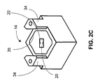
- FIG. 2C is another perspective view of a horn antenna in accordance with the present disclosure.
- FIG. 3A shows a substrate with circuit components in accordance with the present disclosure
- FIG. 3B is a perspective view of a back short on top of the substrate in accordance with the present disclosure.
- FIG. 3C is a perspective view of a back short on top of the substrate mounted in the horn antenna in accordance with the present disclosure
- FIG. 4 is a sectional view showing the coupling of the video output using a ball-grid array in accordance with the present disclosure
- FIG. 5 is a perspective sectional view of a module for an imaging array with cable connectors in accordance with the present disclosure.
- FIG. 6 is a perspective view of a module for an imaging array in accordance with the present disclosure.
- FIG. 1A the millimeter wave receiving side of an imaging focal plane array 10 , in accordance with the present disclosure, is shown.
- FIG. 1B shows the output side of the focal plane array.
- Millimeter wave modules 11 which form the imaging focal plane array, are held in a frame 12 fastened together by screws 15 .
- Each millimeter wave module 11 is configured to provide one pixel of the imaging focal plane array and each module includes a horn antenna 14 to collect millimeter wave signals, a detector to detect the video signal in the millimeter wave signals, and a video output adapter, which provides for connecting the detected video signal to a post processor (not shown).
- the video output adapters 16 are shown as cable connectors; however, there are other embodiments of video output adapters as further described below.
- the detector is located within the millimeter wave module between the input to the horn antenna and the video output adapters, as described further below.
- the overall size of the exemplary 8 ⁇ 8 imaging array shown in FIGS. 1A and 1B can be approximately 4.8 cm ⁇ 4.8 cm, not including the frame 12 .
- the individual millimeter wave modules 11 may have a horn antenna cross section area that is about 6 mm ⁇ 6 mm, which corresponds to two wavelengths at about 100 GHz. This dimension provides acceptable pixel resolution for millimeter wave imaging. Smaller size modules with smaller horn antenna cross section areas are also possible.
- FIGS. 1A and 1B show an 8 ⁇ 8 array, much larger arrays, such as 1024 ⁇ 1024 arrays are possible.
- FIGS. 2A and 2B show a detailed perspective view of the front and back of an exemplary horn antenna 14 , respectively.
- the horn antenna can be made using low-cost manufacturing techniques such as electro-deposition or metal injection molding.
- the input cross-section area of the horn antenna is the dimension of side 21 times the dimension of side 23 .
- sides 21 and 23 may each be 6 millimeters. Sides 21 and 23 can also be less than 6 millimeters.
- the sides of the horn antenna, such as side 25 are configured so that the cross section area of the horn antenna at any section taken along the side, never exceeds the cross section area defined by sides 21 and 23 .
- the cross section area of millimeter wave module 11 which as described above includes the horn antenna, a detector, and a video output adapter, also never exceeds the cross section area defined by sides 21 and 23 . This ensures that the millimeter wave module 11 can be used to build any size focal plane array 10 .
- the horn antenna 14 is shown to have ridged waveguide transitions 24 , which are raised portions that provide for wider bandwidth operation.
- a millimeter wave signal received by the horn antenna is focused by the horn antenna into opening 20 .
- the opening 20 shown in FIG. 2A , is generally circular; however, it is also ridged as shown by ridges 22 , which are located on either side of the opening near the center of opening 20 and are aligned with the ridged waveguide transitions 24 , which connect to the ridges 22 .
- the ridges 22 together with the ridged waveguide transitions 24 enhance the wideband operation of the module.
- FIG. 2B shows the rear side of an exemplary horn antenna 14 .
- a recess 35 is located on the rear side of the horn antenna and the recess is configured so that a detector substrate piece 40 , shown in FIG. 3A , can be inserted into the recess 35 .
- the recess 35 ensures that the detector substrate piece, which includes a detector 60 , is properly aligned relative to the signal input from the opening 20 .
- the tabs 34 on the horn antenna are configured to mate to a video output piece described below.
- FIG. 2C shows another embodiment of the horn antenna 14 with an essentially rectangular opening 36 rather than essentially circular opening 20 shown in FIG. 2B .
- the opening 20 of FIG. 2C also has ridges 22 to provide for wider bandwidth operation.
- the detector substrate piece 40 shown in FIG. 3A includes a substrate 51 that contains thin-film printed circuit probes 42 and 44 that receive the signal from the horn antenna 14 opening 20 .
- the circuit probes 42 and 44 provide the signal to a diode 60 , which can be flip-chip mounted onto the substrate 51 or can be wire-bonded to the substrate 51 .
- the diode detects a video signal and, as shown, video output lines 48 and 50 on the substrate 51 carry the video output from the diode 60 to two video output contact pads 52 and 54 to provide a differential video signal output.
- Some applications can also have a single video output rather than differential.
- the diode 60 can be a Sb-heterostructure diode, which allows for unamplified detection of millimeter wave frequencies from 70 GHz to 150 GHz. This reduces the volume otherwise required by a monolithic microwave integrated circuit (MMIC) low-noise preamplifier. The cost of a low-noise preamplifier is also saved. Other diodes that require amplification may also be used.
- MMIC monolithic microwave integrated circuit
- the substrate 51 is laser machined to a shape that matches the shape of recess 35 on the rear of the horn antenna 14 .
- the dimensions of recess 35 and substrate 51 are well within the cross section of the horn antenna.
- the substrate that contains the detector has a cross section area that is less than or equal to the cross section area of the horn antenna.
- the substrate 51 can typically be alumina, quartz, or other millimeter wave substrate materials of the appropriate thickness.
- the thin-film printed circuit on the substrate 51 is fabricated using commercially available techniques. Plated holes 53 provide electrical interconnects between the top and the bottom of the substrate 51 .
- FIG. 3B shows a back short 66 placed over the detector substrate piece 40
- FIG. 3C shows this combination mounted in the recess 35
- the back short 66 is put on top of the detector substrate piece 40 to provide an impedance match and termination for the signal from the horn antenna 14 .
- the back short 66 can be fabricated as a separate piece of metal and then is attached to the detector substrate piece 40 on plated holes 53 , which provide alignment for the back short 66 , as well as the electrical interconnect discussed above between the top and the bottom of the substrate 51 .
- the detector substrate piece 40 with the back short piece 66 is then attached into the recess 35 using either solder or conductive epoxy, as shown in FIG. 3C . This assembly process can be performed using automated pick-and-place machines.
- FIG. 4 shows one embodiment for a video output adapter and is a half of a cross section along the video output line 48 on the substrate 51 that leads to the video output contact pad 52 .
- a video output piece 30 is configured to mate with the horn antenna 14 and is placed over the rear of the horn antenna 14 .
- the cross section area of the video output piece 30 is less than or equal to the cross section area of the horn antenna.
- a hole 75 is fabricated in the video support piece 30 and is centered on the center of video output contact pad 52 .
- Teflon or another non-conducting material is formed into a sleeve 78 that is inserted into the hole 75 and then a conductive pin 76 , which can be metal, is placed in the sleeve.
- the pin can slide in the sleeve and the sleeve 78 insulates the pin 76 from the video output piece 30 .
- gentle contact is made between the pin 76 and the video output contact pad 52 by tiny commercially available springs 74 , such as fuzz-buttons. These springs 74 keep constant pressure on between the video output contact pad 52 and the pin 76 to insure a good electrical contact.
- the other end of the pin is in contact with a ball 80 of a ball grid array on board 82 .
- the board 82 contains a ball for each millimeter wave module 11 in the array and printed circuits to route the signals from each ball 80 to a post processor (not shown).
- connection of the diode 60 to the video output line 48 via flip-chip connection 62 is also shown in FIG. 4 .
- the opening 20 guides the signal to the circuit probes 42 and (not shown) and the signal is terminated by back short 66 to provide an impedance match.
- FIG. 5 shows a perspective cross-sectional view of another embodiment of the video output adapter using cable connectors.
- the video output is similar to that shown in FIG. 4 in that a spring 74 is between pin 76 and video output contact pad 52 .
- the pin 76 instead of the pin 76 , insulated by sleeve 78 , contacting a ball in a ball grid array, the pin 76 contacts a cable connector 90 , which is installed in a shroud 96 .
- the video cable output piece 94 can be mounted on the rear of the horn antenna 14 by screws 98 .
- the cross section area of the video cable output piece 94 is less than or equal to the cross section area of the horn antenna.
- two cable connectors 90 and 92 are provided.
- the cable connectors 90 and 92 can be commercially available snap-on connectors.
- FIG. 6 shows a perspective view of the assembled module using the video output adapter with cable connectors.
- the video output as described above can also be via a ball grid array and other connection techniques can also be employed. Since each module is entirely self-contained from millimeter wave input via the horn antenna 14 to the video output, focal plane imaging arrays can be built and scaled to any array size.
- the module enables low-cost millimeter wave focal plane arrays for millimeter wave imaging cameras.
- the bandwidth of the modules as described by the embodiments above is for millimeter wave frequencies or from 70 GHz to 150 GHz, other operational frequencies can be implemented by scaling the dimensions of this module, along with making appropriate modifications to the waveguide and circuitry.
Landscapes
- Engineering & Computer Science (AREA)
- Radar, Positioning & Navigation (AREA)
- Remote Sensing (AREA)
- Computer Networks & Wireless Communication (AREA)
- Physics & Mathematics (AREA)
- General Physics & Mathematics (AREA)
- Waveguide Aerials (AREA)
Abstract
Description
Claims (37)
Priority Applications (1)
| Application Number | Priority Date | Filing Date | Title |
|---|---|---|---|
| US12/190,453 US8080774B1 (en) | 2008-08-12 | 2008-08-12 | Module for scalable millimeter wave imaging arrays |
Applications Claiming Priority (1)
| Application Number | Priority Date | Filing Date | Title |
|---|---|---|---|
| US12/190,453 US8080774B1 (en) | 2008-08-12 | 2008-08-12 | Module for scalable millimeter wave imaging arrays |
Publications (1)
| Publication Number | Publication Date |
|---|---|
| US8080774B1 true US8080774B1 (en) | 2011-12-20 |
Family
ID=45219200
Family Applications (1)
| Application Number | Title | Priority Date | Filing Date |
|---|---|---|---|
| US12/190,453 Expired - Fee Related US8080774B1 (en) | 2008-08-12 | 2008-08-12 | Module for scalable millimeter wave imaging arrays |
Country Status (1)
| Country | Link |
|---|---|
| US (1) | US8080774B1 (en) |
Cited By (3)
| Publication number | Priority date | Publication date | Assignee | Title |
|---|---|---|---|---|
| US20140254979A1 (en) * | 2013-03-08 | 2014-09-11 | Northrop Grumman Systems Corporation | Waveguide and semiconductor packaging |
| WO2015069520A1 (en) * | 2013-11-05 | 2015-05-14 | Northrop Grumman Systems Corporation | Passive millimeter wave image converter |
| US9437923B2 (en) | 2012-10-15 | 2016-09-06 | The United States of America, as represented by the Secretary of Commerce, The National Institute of Standards and Technology | Simultaneous imaging and precision alignment of two millimeter wave antennas based on polarization-selective machine vision |
Citations (19)
| Publication number | Priority date | Publication date | Assignee | Title |
|---|---|---|---|---|
| US3824593A (en) * | 1972-12-04 | 1974-07-16 | Hughes Aircraft Co | Millimeter wave imaging system using direct carrier injection |
| US3882396A (en) * | 1973-08-10 | 1975-05-06 | Bell Telephone Labor Inc | Impedance-matched waveguide frequency converter integrally mounted on stripline |
| US5237334A (en) * | 1989-06-29 | 1993-08-17 | Waters William M | Focal plane antenna array for millimeter waves |
| US5760397A (en) * | 1996-05-22 | 1998-06-02 | Huguenin; G. Richard | Millimeter wave imaging system |
| US6049313A (en) * | 1997-06-10 | 2000-04-11 | Yupiteru Industries Co., Ltd. | Microwave detector |
| US20020080081A1 (en) * | 2000-12-21 | 2002-06-27 | Kefeng Liu | Diagonal dual-polarized broadband horn antenna |
| US20020149530A1 (en) * | 2001-04-11 | 2002-10-17 | International Business Machines Corporation | Dual damascene horn antenna |
| US6635907B1 (en) * | 1999-11-17 | 2003-10-21 | Hrl Laboratories, Llc | Type II interband heterostructure backward diodes |
| US20030210197A1 (en) * | 2002-05-08 | 2003-11-13 | Lockheed Martin Corporation | Multiple mode broadband ridged horn antenna |
| US6828556B2 (en) * | 2001-09-28 | 2004-12-07 | Hrl Laboratories, Llc | Millimeter wave imaging array |
| US6841768B2 (en) * | 2001-11-09 | 2005-01-11 | Korea Institute Of Science And Technology | Three dimensional conical horn antenna coupled image detector and the manufacturing method thereof |
| US20050009226A1 (en) * | 2002-09-04 | 2005-01-13 | Munehito Kumagai | Silicon substrate device and its manufacturing method |
| US20050270247A1 (en) * | 2002-09-20 | 2005-12-08 | Nobumasa Kitamori | Antenna device and transmitting/receiving device |
| US20060220974A1 (en) * | 2005-03-31 | 2006-10-05 | Denso Corporation | High frequency module and array of the same |
| US20060220952A1 (en) * | 2005-03-30 | 2006-10-05 | Denso Corporation | Electric wave transmitting/receiving module and imaging sensor having electric wave transmitting/receiving module |
| US7135848B1 (en) | 2005-12-12 | 2006-11-14 | Xytrans, Inc. | Highly integrated radiometer sensor cell |
| US20080048922A1 (en) * | 2006-05-24 | 2008-02-28 | Haziza Dedi D | Integrated waveguide antenna array |
| US20090066598A1 (en) * | 2007-09-07 | 2009-03-12 | Tyco Electronics Corporation And M/A-Com, Inc. | Modular waveguide feed horn |
| US7583074B1 (en) * | 2005-12-16 | 2009-09-01 | Hrl Laboratories, Llc | Low cost millimeter wave imager |
-
2008
- 2008-08-12 US US12/190,453 patent/US8080774B1/en not_active Expired - Fee Related
Patent Citations (23)
| Publication number | Priority date | Publication date | Assignee | Title |
|---|---|---|---|---|
| US3824593A (en) * | 1972-12-04 | 1974-07-16 | Hughes Aircraft Co | Millimeter wave imaging system using direct carrier injection |
| US3882396A (en) * | 1973-08-10 | 1975-05-06 | Bell Telephone Labor Inc | Impedance-matched waveguide frequency converter integrally mounted on stripline |
| US5237334A (en) * | 1989-06-29 | 1993-08-17 | Waters William M | Focal plane antenna array for millimeter waves |
| US5760397A (en) * | 1996-05-22 | 1998-06-02 | Huguenin; G. Richard | Millimeter wave imaging system |
| US6049313A (en) * | 1997-06-10 | 2000-04-11 | Yupiteru Industries Co., Ltd. | Microwave detector |
| US6635907B1 (en) * | 1999-11-17 | 2003-10-21 | Hrl Laboratories, Llc | Type II interband heterostructure backward diodes |
| US20020080081A1 (en) * | 2000-12-21 | 2002-06-27 | Kefeng Liu | Diagonal dual-polarized broadband horn antenna |
| US20020149530A1 (en) * | 2001-04-11 | 2002-10-17 | International Business Machines Corporation | Dual damascene horn antenna |
| US6828556B2 (en) * | 2001-09-28 | 2004-12-07 | Hrl Laboratories, Llc | Millimeter wave imaging array |
| US6841768B2 (en) * | 2001-11-09 | 2005-01-11 | Korea Institute Of Science And Technology | Three dimensional conical horn antenna coupled image detector and the manufacturing method thereof |
| US20030210197A1 (en) * | 2002-05-08 | 2003-11-13 | Lockheed Martin Corporation | Multiple mode broadband ridged horn antenna |
| US20050009226A1 (en) * | 2002-09-04 | 2005-01-13 | Munehito Kumagai | Silicon substrate device and its manufacturing method |
| US7081370B2 (en) * | 2002-09-04 | 2006-07-25 | Mitsubishi Denki Kabushiki Kaisha | Silicon substrate apparatus and method of manufacturing the silicon substrate apparatus |
| US20050270247A1 (en) * | 2002-09-20 | 2005-12-08 | Nobumasa Kitamori | Antenna device and transmitting/receiving device |
| US7064726B2 (en) * | 2002-09-20 | 2006-06-20 | Murata Manufacturing Co., Ltd. | Antenna device and transmitting/receiving device |
| US20060220952A1 (en) * | 2005-03-30 | 2006-10-05 | Denso Corporation | Electric wave transmitting/receiving module and imaging sensor having electric wave transmitting/receiving module |
| US20060220974A1 (en) * | 2005-03-31 | 2006-10-05 | Denso Corporation | High frequency module and array of the same |
| US7245264B2 (en) * | 2005-03-31 | 2007-07-17 | Denso Corporation | High frequency module and array of the same |
| US7135848B1 (en) | 2005-12-12 | 2006-11-14 | Xytrans, Inc. | Highly integrated radiometer sensor cell |
| US7583074B1 (en) * | 2005-12-16 | 2009-09-01 | Hrl Laboratories, Llc | Low cost millimeter wave imager |
| US7795859B1 (en) * | 2005-12-16 | 2010-09-14 | Hrl Laboratories, Llc | Low cost millimeter wave imager |
| US20080048922A1 (en) * | 2006-05-24 | 2008-02-28 | Haziza Dedi D | Integrated waveguide antenna array |
| US20090066598A1 (en) * | 2007-09-07 | 2009-03-12 | Tyco Electronics Corporation And M/A-Com, Inc. | Modular waveguide feed horn |
Non-Patent Citations (2)
| Title |
|---|
| Kane, B., et al., "High Sensitivity W-Band MMIC Radiometer Modules,"IEEE 1995 Microwave and Millimeter-Wave Monolithic Circuits Symposium, pp. 59-62 (1995). |
| Yngvesson, K.S., et al., "The Tapered Slot Antenna-A New Integrated Element for Millimeter-Wave Applications," IEEE Transactions on Microwave theory and Techniques, vol. 37, No. 2, (Feb. 1989). |
Cited By (5)
| Publication number | Priority date | Publication date | Assignee | Title |
|---|---|---|---|---|
| US9437923B2 (en) | 2012-10-15 | 2016-09-06 | The United States of America, as represented by the Secretary of Commerce, The National Institute of Standards and Technology | Simultaneous imaging and precision alignment of two millimeter wave antennas based on polarization-selective machine vision |
| US20140254979A1 (en) * | 2013-03-08 | 2014-09-11 | Northrop Grumman Systems Corporation | Waveguide and semiconductor packaging |
| US9478458B2 (en) * | 2013-03-08 | 2016-10-25 | Northrop Grumman Systems Corporation | Waveguide and semiconductor packaging |
| US9960204B2 (en) * | 2013-03-08 | 2018-05-01 | Northrop Grumman Systems Corporation | Waveguide and semiconductor packaging |
| WO2015069520A1 (en) * | 2013-11-05 | 2015-05-14 | Northrop Grumman Systems Corporation | Passive millimeter wave image converter |
Similar Documents
| Publication | Publication Date | Title |
|---|---|---|
| US7795859B1 (en) | Low cost millimeter wave imager | |
| EP3803474B1 (en) | Highly integrated miniature radiometer chip | |
| US6980068B2 (en) | System for and method of interconnecting high-frequency transmission lines | |
| JPH0730133A (en) | Electro-optical assembly | |
| US11662363B2 (en) | Test socket assembly with antenna and related methods | |
| US8547278B2 (en) | Sensing device having multi beam antenna array | |
| EP1097488A1 (en) | Rf connector | |
| US20130330944A1 (en) | Spring-loaded blind-mate electrical interconnect | |
| US8080774B1 (en) | Module for scalable millimeter wave imaging arrays | |
| US20040264980A1 (en) | Optical receiver module with To-Can structure | |
| US7460060B2 (en) | Electromagnetic wave transmitting/receiving module and imaging sensor having electromagnetic wave transmitting/receiving module | |
| EP1026742A3 (en) | Solder ball grid array for connecting multiple millimeter wave assemblies | |
| US6781108B2 (en) | Noise canceling photosensor-amplifier device | |
| US7496271B2 (en) | Printed circuit board with recessed region | |
| SE528289C2 (en) | Antenna with coaxial connector | |
| CN101776750B (en) | Integrated high-sensitivity millimeter wave receiver for millimeter wave array imaging system | |
| US20160143143A1 (en) | Optoelectronic modules and assemblies comprising optoelectronic modules | |
| JP2005073242A (en) | Dielectric resonator, dielectric filter, and method for supporting dielectric resonator element | |
| CN110132425B (en) | Radiometer front end and terminal equipment | |
| CN115616669A (en) | A multi-channel integrated dual-polarization passive radio frequency receiving device and method | |
| CN110187195B (en) | Radiometer front-end and terminal equipment | |
| US20020070739A1 (en) | Apparatus and method to read output information from a backside of a silicon device | |
| Schaffner et al. | A wideband radiometer module for an unamplified direct detection scalable W-band imaging array | |
| TW569006B (en) | Millimeter wave imaging array | |
| US20170084523A1 (en) | On-package connector |
Legal Events
| Date | Code | Title | Description |
|---|---|---|---|
| AS | Assignment |
Owner name: HRL LABORATORIES, LLC, CALIFORNIA Free format text: ASSIGNMENT OF ASSIGNORS INTEREST;ASSIGNORS:GUINN, KEITH V.;SCHAFFNER, JAMES H.;SIGNING DATES FROM 20080802 TO 20080812;REEL/FRAME:021392/0393 |
|
| FEPP | Fee payment procedure |
Free format text: PAYOR NUMBER ASSIGNED (ORIGINAL EVENT CODE: ASPN); ENTITY STATUS OF PATENT OWNER: LARGE ENTITY |
|
| ZAAA | Notice of allowance and fees due |
Free format text: ORIGINAL CODE: NOA |
|
| ZAAB | Notice of allowance mailed |
Free format text: ORIGINAL CODE: MN/=. |
|
| STCF | Information on status: patent grant |
Free format text: PATENTED CASE |
|
| FPAY | Fee payment |
Year of fee payment: 4 |
|
| MAFP | Maintenance fee payment |
Free format text: PAYMENT OF MAINTENANCE FEE, 8TH YEAR, LARGE ENTITY (ORIGINAL EVENT CODE: M1552); ENTITY STATUS OF PATENT OWNER: LARGE ENTITY Year of fee payment: 8 |
|
| FEPP | Fee payment procedure |
Free format text: MAINTENANCE FEE REMINDER MAILED (ORIGINAL EVENT CODE: REM.); ENTITY STATUS OF PATENT OWNER: LARGE ENTITY |
|
| LAPS | Lapse for failure to pay maintenance fees |
Free format text: PATENT EXPIRED FOR FAILURE TO PAY MAINTENANCE FEES (ORIGINAL EVENT CODE: EXP.); ENTITY STATUS OF PATENT OWNER: LARGE ENTITY |
|
| STCH | Information on status: patent discontinuation |
Free format text: PATENT EXPIRED DUE TO NONPAYMENT OF MAINTENANCE FEES UNDER 37 CFR 1.362 |
|
| FP | Lapsed due to failure to pay maintenance fee |
Effective date: 20231220 |