US8080366B2 - In-line process for making thin film electronic devices - Google Patents
In-line process for making thin film electronic devices Download PDFInfo
- Publication number
- US8080366B2 US8080366B2 US11/709,785 US70978507A US8080366B2 US 8080366 B2 US8080366 B2 US 8080366B2 US 70978507 A US70978507 A US 70978507A US 8080366 B2 US8080366 B2 US 8080366B2
- Authority
- US
- United States
- Prior art keywords
- line process
- layer
- process according
- patternable
- substrate
- Prior art date
- Legal status (The legal status is an assumption and is not a legal conclusion. Google has not performed a legal analysis and makes no representation as to the accuracy of the status listed.)
- Expired - Fee Related, expires
Links
Images


Classifications
-
- H—ELECTRICITY
- H10—SEMICONDUCTOR DEVICES; ELECTRIC SOLID-STATE DEVICES NOT OTHERWISE PROVIDED FOR
- H10P—GENERIC PROCESSES OR APPARATUS FOR THE MANUFACTURE OR TREATMENT OF DEVICES COVERED BY CLASS H10
- H10P95/00—Generic processes or apparatus for manufacture or treatments not covered by the other groups of this subclass
-
- H—ELECTRICITY
- H10—SEMICONDUCTOR DEVICES; ELECTRIC SOLID-STATE DEVICES NOT OTHERWISE PROVIDED FOR
- H10P—GENERIC PROCESSES OR APPARATUS FOR THE MANUFACTURE OR TREATMENT OF DEVICES COVERED BY CLASS H10
- H10P72/00—Handling or holding of wafers, substrates or devices during manufacture or treatment thereof
- H10P72/04—Apparatus for manufacture or treatment
- H10P72/0448—Apparatus for applying a liquid, a resin, an ink or the like
-
- H—ELECTRICITY
- H10—SEMICONDUCTOR DEVICES; ELECTRIC SOLID-STATE DEVICES NOT OTHERWISE PROVIDED FOR
- H10D—INORGANIC ELECTRIC SEMICONDUCTOR DEVICES
- H10D86/00—Integrated devices formed in or on insulating or conducting substrates, e.g. formed in silicon-on-insulator [SOI] substrates or on stainless steel or glass substrates
- H10D86/01—Manufacture or treatment
- H10D86/021—Manufacture or treatment of multiple TFTs
- H10D86/0231—Manufacture or treatment of multiple TFTs using masks, e.g. half-tone masks
-
- H—ELECTRICITY
- H10—SEMICONDUCTOR DEVICES; ELECTRIC SOLID-STATE DEVICES NOT OTHERWISE PROVIDED FOR
- H10D—INORGANIC ELECTRIC SEMICONDUCTOR DEVICES
- H10D86/00—Integrated devices formed in or on insulating or conducting substrates, e.g. formed in silicon-on-insulator [SOI] substrates or on stainless steel or glass substrates
- H10D86/40—Integrated devices formed in or on insulating or conducting substrates, e.g. formed in silicon-on-insulator [SOI] substrates or on stainless steel or glass substrates characterised by multiple TFTs
- H10D86/60—Integrated devices formed in or on insulating or conducting substrates, e.g. formed in silicon-on-insulator [SOI] substrates or on stainless steel or glass substrates characterised by multiple TFTs wherein the TFTs are in active matrices
-
- H—ELECTRICITY
- H10—SEMICONDUCTOR DEVICES; ELECTRIC SOLID-STATE DEVICES NOT OTHERWISE PROVIDED FOR
- H10K—ORGANIC ELECTRIC SOLID-STATE DEVICES
- H10K71/00—Manufacture or treatment specially adapted for the organic devices covered by this subclass
-
- H—ELECTRICITY
- H10—SEMICONDUCTOR DEVICES; ELECTRIC SOLID-STATE DEVICES NOT OTHERWISE PROVIDED FOR
- H10P—GENERIC PROCESSES OR APPARATUS FOR THE MANUFACTURE OR TREATMENT OF DEVICES COVERED BY CLASS H10
- H10P72/00—Handling or holding of wafers, substrates or devices during manufacture or treatment thereof
- H10P72/04—Apparatus for manufacture or treatment
- H10P72/0451—Apparatus for manufacturing or treating in a plurality of work-stations
- H10P72/0452—Apparatus for manufacturing or treating in a plurality of work-stations characterised by the layout of the process chambers
- H10P72/0456—Apparatus for manufacturing or treating in a plurality of work-stations characterised by the layout of the process chambers in-line arrangement
-
- H—ELECTRICITY
- H10—SEMICONDUCTOR DEVICES; ELECTRIC SOLID-STATE DEVICES NOT OTHERWISE PROVIDED FOR
- H10P—GENERIC PROCESSES OR APPARATUS FOR THE MANUFACTURE OR TREATMENT OF DEVICES COVERED BY CLASS H10
- H10P72/00—Handling or holding of wafers, substrates or devices during manufacture or treatment thereof
- H10P72/04—Apparatus for manufacture or treatment
- H10P72/0451—Apparatus for manufacturing or treating in a plurality of work-stations
- H10P72/0464—Apparatus for manufacturing or treating in a plurality of work-stations characterised by the construction of the transfer chamber
-
- H—ELECTRICITY
- H10—SEMICONDUCTOR DEVICES; ELECTRIC SOLID-STATE DEVICES NOT OTHERWISE PROVIDED FOR
- H10P—GENERIC PROCESSES OR APPARATUS FOR THE MANUFACTURE OR TREATMENT OF DEVICES COVERED BY CLASS H10
- H10P72/00—Handling or holding of wafers, substrates or devices during manufacture or treatment thereof
- H10P72/04—Apparatus for manufacture or treatment
- H10P72/0451—Apparatus for manufacturing or treating in a plurality of work-stations
- H10P72/0468—Apparatus for manufacturing or treating in a plurality of work-stations comprising a chamber adapted to a particular process
- H10P72/0474—Apparatus for manufacturing or treating in a plurality of work-stations comprising a chamber adapted to a particular process comprising at least one lithography chamber
-
- H—ELECTRICITY
- H10—SEMICONDUCTOR DEVICES; ELECTRIC SOLID-STATE DEVICES NOT OTHERWISE PROVIDED FOR
- H10K—ORGANIC ELECTRIC SOLID-STATE DEVICES
- H10K59/00—Integrated devices, or assemblies of multiple devices, comprising at least one organic light-emitting element covered by group H10K50/00
- H10K59/10—OLED displays
- H10K59/12—Active-matrix OLED [AMOLED] displays
Definitions
- the present invention relates to an in-line process for making a thin film electronic device on a substrate.
- the thin film electronic device is a thin film transistor.
- this process is integrated in and in-line process for making flat panel displays.
- a flat panel display comprises an array of pixels on a substrate.
- the pixels may comprise liquid crystals, or organic light emitting diodes, or OLEDs.
- OLEDs organic light emitting diodes
- a picture is formed by selectively activating pixels within the grid. The picture quality and resolution is determined to a large extent by the level of sophistication of the system for driving the pixels.
- the segment drive method is designed to apply a voltage to discrete groups of pixels at the same time. This method is suitable for simple displays such as those in calculators, but are unsuitable for more sophisticated displays because of their relatively poor resolution.
- a form of matrix drive method is required.
- Two types of drive method are used for matrix displays. In the static, or direct, drive method each pixel is individually wired to a driver. This is a simple driving method, but as the number of pixels is increased the wiring becomes very complex.
- An alternative method is the multiplex method, in which the pixels are arranged and wired in a matrix format. There are two types of matrix format, passive matrix and active matrix.
- each pixel is activated more than one frame time.
- the effective voltage applied to the pixel must average the signal pulses over several frame times, which results in a slow response time and a reduction of the maximum contrast ratio.
- the addressing of a passive matrix display also results in cross-talk that produces blurred images, because non-selected pixels are driven through a secondary signal voltage path.
- In-active matrix displays a switching device and a combined storage capacitor can be integrated at each cross point of the electrodes, such that each pixel has at least one switching device.
- Active matrix displays have no inherent limitation in the number of scan lines, and present fewer cross-talk issues.
- Most active matrix displays use switching devices that are transistors made of deposited thin films, known as thin film transistors or TFTs.
- a suitable semiconducting material is doped silicon. If doped silicon is used, it is usually in the form of amorphous silicon (a-Si). Amorphous silicon TFTs can be made in large area fabrication at a relatively low temperature (300 to 400 degrees C.).
- Poly-crystalline silicon (p-Si) or microcrystalline silicon (mc-Si) is superior to amorphous silicon in that It has an electron mobility that is 1 or 2 orders of magnitude greater than that of amorphous silicon.
- polycrystalline and microcrystalline silicon are costly to make and especially difficult to fabricate when manufacturing large area displays.
- TFT TFT-transistive field-effect transistor
- the creation of a TFT requires a significant number of individual process steps, each of which needs to be carried out in a vacuum or a controlled atmosphere in order to avoid contamination. Even small amounts of contamination may seriously hamper or even destroy the functionality of the TFT.
- the creation of a flat panel display requires additional steps of depositing materials, such as the display materials themselves and encapsulation layers protecting the TFTs and display materials from ambient influences.
- an object of the present invention to provide an in-line process for the manufacture of thin film transistors on a substrate. It is a further object of the present invention to integrate the in-line process for manufacturing thin film transistors into an in-line process for manufacturing flat panel displays.
- the invention relates to an in-line process for making a thin film electronic device on a substrate, comprising the steps of:
- steps being carried out without intermediate exposure of the substrate to ambient air.
- the first pattern in which the patternable material is deposited can be a layer fully covering the structurable layer.
- This full layer may be subsequently developed into a second pattern, for example by covering the layer with a mask, and curing the exposed areas of the patternable layer by, for example irradiation.
- the patternable material is deposited in a first pattern approximating said second pattern, and subsequently cured into the desired second pattern, which is inscribed within the first pattern.
- the second pattern may be formed by ablation of parts of the first pattern.
- the thin film electronic device is a thin film transistor.
- the invention relates to a process for manufacturing a flat panel display incorporating the in-line process for making thin film transistors on a substrate, whereby the TFTs are formed on the substrate arranged in a pixel pattern, and the formation of the thin film transistors is followed by the steps of:
- liquid crystals between two glass plates may be deposited onto the TFTs.
- in-line process means a process comprising several process steps that need to be carried out in a vacuum or in a controlled atmosphere, whereby these process steps are carried out in interconnected process stations, such that the substrate is not exposed to ambient air during or in-between process steps.
- a preferred thin film electronic device is a thin film transistor.
- substrate in this context is intended to encompass known glass and silicon substrates as well as polymer substrates and other suitable materials on which the inline process of the invention may be performed.
- the in-line process is continuous in the sense that subsequent process steps follow one another without intermediate storage of the substrate, other than small buffers for short-term storage.
- ambient air means air suitable for the breathing needs of human beings. As such the term encompasses outside air, conditioned air as may be found inside a building, and conditioned and purified air as may be found in a clean room.
- the structurable layer may be an insulating layer, a metal layer, a layer of a transparent conducting oxide (TCO), a semiconducting layer or any other layer that may be suitably structured to form part of the thin film electronic device.
- a preferred semiconducting material for the structurable layer is doped silicon.
- the structurable layer may be deposited using an evaporation process, preferably a plasma-enhanced chemical vapor deposition (PECVD) process, or a sputtering process.
- PECVD plasma-enhanced chemical vapor deposition
- etching is intended to mean any appropriate technique for removing material or otherwise changing its properties.
- patternable layer is intended to mean any layer that may be applied or formed on the structurable layer and that may form a pattern or may be treated to cause a pattern to be formed.
- a preferred form of patternable material is photoresist material that may be cured e.g. by exposure to light and then developed.
- Other forms of patterning are also known e.g. where part of an active layer is removed by laser ablation. Such a process is known from the unpublished PCT application PCT/IL2004/000792, the contents of which are hereby incorporated by reference in their entirety.
- Further alternative processes that permit a fine pattern to be formed in a layer may also be used, In particular, surface energy patterning techniques and other modifications of the surface properties of the patternable layer e.g. under influence of illumination
- the patternable material is used for selectively covering the structurable layer, so that this layer may be structured by, for example, by etching away the exposed portions of the structurable layer.
- the patternable material may be deposited in a first pattern, and subsequently selectively cured in a second pattern, inscribed within the first pattern.
- the term “cured” is intended to cover any process that may distinguish the properties of part of the patternable layer and encompasses conventional negative and positive photoresist and also laser ablation techniques for forming the second pattern.
- the first pattern may be a full layer, completely covering the structurable layer. Any known technique may be used for depositing the layer of patternable material. For use with photoresist material, curing of selected areas of this layer may be done by irradiation through a mask. Uncured photoresist material is then removed in a developing process, resulting in the desired second pattern.
- Selective patterning of the patternable material may also be accomplished using a direct imaging technique.
- the first pattern is not a full layer, but approximates the desired structure of the structurable layer.
- the patternable material is selectively removed to form the desired second pattern. It will be clear that the first pattern must be such that the second pattern can be inscribed within the first pattern.
- a preferred technique for depositing the patternable material in a first pattern that is less than a full layer is a printing technique, whereby the patternable material is deposited using a printhead. Advantages of such a technique is that less patternable material is used, and less patternable material needs to be removed in the following step.
- the patternable material is deposited and cured using an integrated printhead/cure head assembly.
- Such an assembly may sometimes be referred to as a processing head.
- the position of the cure head may be, moreover, directly mechanically coupled to the position of the printhead.
- the direct coupling of the position of the print head with the cure head practically excludes the possibility of the cure head carrying out a curing operation at incorrect positions on the substrate. With a localised curing step, any relatively inaccurate outlines of the patternable material applied by the printer can be more easily “cut off”, so that cured structures with fine, sharp boundaries are obtained.
- a scanning step can be carried out immediately prior to the printing step by a first scan head provided on the processing head on an upstream side of the printhead, viewed in the relative direction of movement of the processing head with respect to the substrate.
- a scanning step can be carried out immediately after the printing step e.g. by a second scan head provided on the processing head on a downstream side of the printhead, viewed in the relative direction of movement of the processing head with respect to the substrate.
- a second scan head provided on the processing head on a downstream side of the printhead, viewed in the relative direction of movement of the processing head with respect to the substrate.
- the head can go through a forward and backward movement over the same area of the substrate. Should it be detected during the second scanning movement that for some areas the patternable material has not yet been applied, it can still be deposited and cured in those areas in the backward movement.
- a scanning step is carried out immediately prior to the cure step in that a first scan head is provided on the processing head on the upstream side of the cure head, viewed in the relative direction of movement of the processing head with respect to the substrate.
- a scanning step is carried out immediately after the curing step e.g. by a second scan head provided on the processing head on the downstream side of the cure head, viewed in the relative direction of movement of the processing head with respect to the substrate.
- a second scan head provided on the processing head on the downstream side of the cure head, viewed in the relative direction of movement of the processing head with respect to the substrate.
- the head can go through a forward and a backward movement over the same area of the substrate. If it is detected with the second scan head that the patternable material has not yet been cured in some areas, it can still be cured in those areas in the backward movement.
- the in-line process of the present invention preferably is a continuous process. More preferably the process comprises in-line quality checks, and feedback loops for adjusting selected process parameters based on these in-line quality checks.
- the process optionally comprises process steps selected from the group of a washing step; a pre-bake step of the patternable layer; a post-bake step of the patternable layer; a structured layer annealing step; and combinations thereof.
- the process for making a thin film electronic device may be incorporated in a process for making a flat panel display.
- the in-line process of the present invention is used for depositing onto a substrate thin film transistors that are arranged as pixels.
- this process is integrated with an in-line process for printing organic light emitting material in discrete areas associated with these pixels.
- this process is followed by an in-line process for providing a cathode to the organic light emitting material to form an OLED device, and for covering said OLED device with encapsulating layers.
- pixels capable of emitting light of different colors may be accomplished by combining in each pixel organic light emitting materials capable of emitting light of different colors.
- Another possibility is to provide an organic light emitting material emitting light of one color, preferably white, and providing color filters or a phosphorescing material.
- the organic light emitting material may be deposited using an evaporation technique or a printing technique.
- the color filters and the phosphorescing material are preferably applied using a printing technique.
- the process may comprise feedback loops based on in-line quality checks.
- an assembly for processing substrates which assembly comprises a vacuum load lock and at least one process chamber.
- vacuum encompasses both an air pressure that is greatly reduced from atmospheric pressure, as well as controlled, specialized environments, such as carefully purified air and inert gases.
- the assembly comprises a series of process chambers, each process chamber being dedicated to a specific process step.
- the assembly further comprises conveying means for conveying a substrate between neighbouring process chambers.
- the apparatus for performing the process of the present invention is modular, and comprises an in-line module for making thin film transistors on a substrate, an in-line module for printing light emitting material onto the substrate, and an in-line module for providing a cathode and encapsulating layers.
- the apparatus may further comprise an in-line module for applying color filters, or an in-line module for applying phosphorescing material.
- the various modules may be stand-alone modules, in which case they may be assembled in a common clean room.
- the various modules are connected by connecting vacuum chambers, each connecting vacuum chamber having conveying means for conveying a substrate to a neighbouring module.
- the assembly is provided with a conveying device for moving the substrates from a vacuum lock to a process chamber.
- a conveying device for moving the substrates from a vacuum lock to a process chamber.
- the assembly comprises a number of process chambers, each dedicated to a specific process step.
- a conveying device is provided for moving the substrates from the vacuum lock to the first process chamber, and successively to subsequent process chambers. After completion of the final process step in the last process chamber, the substrate is moved to a vacuum lock from where it can be removed from the assembly.
- a preferred assembly is disclosed in Netherlands patent application number 102 4215, filed Sep. 3, 2003, the disclosures of which are incorporated herein by reference.
- the in-line process of the present invention preferably comprises at least one step involving the deposition of silicon nitrides. It is desirable to use a source that is capable of depositing silicon nitrides at a high deposition speed, as otherwise such a process step could become the rate determining step for the entire in-line process.
- European patent number EP 0 297 637 discloses a plasma source that is capable of depositing silicon nitrides with deposition speeds on the order of tens of nm per second. This plasma source is particularly preferred for use in silicon nitride deposition steps of the in-line process of the present invention.
- the disclosures of European patent number EP 0 297 637 are incorporated herein by reference.
- a particularly preferred plasma source is disclosed in Netherlands patent application 102 3491, filed May 21, 2003, the disclosures of which are incorporated herein by reference.
- FIG. 1 is a schematic comparison of a batch process, a semi-batch process, and the in-line process of the present invention.
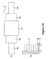
- FIG. 1A is a more detailed representation of a process step station as may be used in a batch or semi-batch process.
- FIG. 2 is a schematic cross sectional view of a device manufactured by the process of the present invention.
- FIG. 3 is a schematic representation of the process steps for making a structured layer.
- FIG. 4 is a schematic representation of an integrated printhead/cure head/scan head assembly.
- FIG. 5 shows part of a module for making depositing a structured layer on a substrate.
- FIG. 6 shows a complete modular apparatus for making a flat screen display panel.
- FIG. 1 compares the principles of a batch process for the manufacture of, for example, a TFT, with what could be considered a semi-batch process, and with the in-line process of the present invention.
- a process in relation to a technique using a photoresist layer is described, it is intended that this be interpreted to apply equally to other patternable layers.
- Section A of FIG. 1 is a schematic depiction of a batch process.
- the various steps of the manufacturing process are carried out in dedicated devices, each represented by a rectangular block.
- the devices are placed in a common clean room, 10 .
- Devices 11 a , 11 b , and 11 c are identical, and may be operating simultaneously.
- the arrows depict, schematically, the flow of a product through the manufacturing process.
- An important feature of the batch manufacturing process is the cross-over of product from one “assembly line” to another, as illustrated by crossing arrows 12 a and 12 b.
- Another important feature is the presence of redundant capacity at certain stages of the manufacturing process, which is the result of the fact that the capacities of individual devices are not always attuned to each other. Also, the designers of batch processes may have a need for building spare capacity into their process in order to be able to deal with imbalances in the process logistics, and with occasional equipment breakdowns.
- This feature of the batch process is illustrated by rectangular boxes that do not have incoming or outgoing arrows.
- An aspect of the batch process is the use of batch wise loadlocking of the substrates, leading to variation in history before the substrates are processed.
- Yet another feature of the batch process is the fact that product may need to be stored in clean room 10 for some length of time while waiting for a device dedicated to the next process step to become available. This feature is not shown in FIG. 1 .
- Section B of FIG. 1 shows what could be considered a “semi-batch” process.
- dedicated devices depicted by rectangular boxes are placed together in a common clean room.
- semi-batch process there typically is one such device for each process step.
- the product flows from one device to the next, as shown by the arrows.
- product may have to be stored in the clean room for some length of time while waiting for the device for the next process step to become available. This is not shown in FIG. 1 .
- Section C of FIG. 1 shows schematically an in-line process according to the present invention.
- the rectangular boxes represent modules of an integrated manufacturing unit.
- the modules are interconnected, and the product is conveyed from one module to the next by a conveying means (not shown).
- a load-lock is integrated in the manufacturing unit.
- As the modules are interconnected there is no need for the modules to be placed in a clean room environment.
- As the product is not exposed to an ambient environment in between process steps, the time lost in preparing the product for each subsequent process step is much reduced as compared to both the batch and the semi-batch processes.
- the production capacities of the individual modules are attuned to one another, so that the amount of idle time between process steps is much reduced as compared to both the batch and the semi-batch processes.
- Another advantage of the in-line process is that all substrates have the same process history, resulting in a much reduced product variability as compared to products made by a batch process or a semi-batch process.
- FIG. 1A shows in more detail one of the modules 11 a , 11 b , 11 c.
- Module 11 comprises docking stations 13 a , 13 b ; load locks 14 a and 14 b ; and process chamber 15 .
- FIG. 1A Portion b of FIG. 1A shows a so-called Automated Guide Vehicle (AGV) 16 , which is used for transporting container 18 , which holds a stack of substrates 17 .
- AGV Automated Guide Vehicle
- AGV 16 is moved into docking station 13 a , and from there into load lock 14 a .
- load lock 14 a the substrates are pre-conditioned, and then moved one-by-one into process chamber 15 to undergo a specific process step.
- each substrate has undergone the process step of process chamber 15 it is moved onto an AGV that is waiting in load lock 14 b .
- the AGV is moved from load lock 14 b to docking station 13 b , and from there into the clean room environment (not shown).
- section B of FIG. 1 uses similar modules, resulting in the same kind of variations in process history between individual substrates. These differences accumulate during the various process steps, and may result in significant differences in product quality, even among substrates of one batch.
- FIG. 2 shows a cross section of a preferred light emitting device 20 suitable for use in the flat panel displays made by the process of the present invention.
- Substrate 21 can be any suitable substrate known in the art.
- the preferred substrate is transparent, for example a thin sheet of glass or a transparent polymer.
- a preferred gate composition is a sputtered layer of 100 to 500 nm thickness of a metal, TCO or combination of the two.
- the substrate and the gate are covered by a layer of silicon nitride 23 .
- a layer of a semiconducting material 24 On top of the silicon nitride layer, immediately above the gate 22 , is a layer of a semiconducting material 24 .
- the semiconducting layer 24 may consist of doped versions of amorphous silicon, microcrystalline silicon, or a mixture of polycrystalline silicon and microcrystalline silicon.
- the source layer 25 On top of the silicon nitride layer 23 is the source layer 25 , in contact with the semiconducting layer.
- the source layer 25 which can be a sputtered layer of, for example, a metal like Al, Ag, Au, Mo, Cr, Ti, or an oxide like ZnO or a TCO, has an opening in the area of the semiconducting layer.
- a planarizing layer 26 On top of the entire structure is a planarizing layer 26 .
- anode 27 On top of planarizing layer 26 is anode 27 , which penetrates through the planarizing layer so as to make electrical contact with source layer 25 .
- the anode material may be any conductive material that can be easily deposited by known techniques.
- the anode is a light-reflecting layer of Al, Ag, Au, Mo, Cr, Ti, ZnO or TCO. Aluminum is specifically preferred.
- Light emitting material 28 is deposited on top of anode 27 .
- the light emitting material is preferably an organic light emitting material.
- the organic light emitting material may be a so-called “small molecule” (i.e., non-polymeric) material, or it may be a polymeric light emitting material.
- small molecule material include fluorescent metal chelates, for example 8-hydroxyqulnoline aluminum (Alq3).
- polymeric materials include the conjugated polymers disclosed in U.S. Pat. No. 5,247,190, the disclosures of which are incorporated herein, by reference. Of these polymers, poly(p-phenylenevinylene) (“PPV”) is particularly preferred.
- Cathode 29 is positioned on top of the light emitting material 28 , in the area immediately above the TFT. Shown in FIG. 2 also is blocking layer 30 , which prevents light from reaching the TFT and influencing its operation. This blocking layer is optional.
- Gate 22 , silicon layer 24 , source layer 25 , planarizing layer 26 , anode 27 , and blocking layer 30 are structured layers.
- the TFT, the anode, the cathode and the light emitting material form the functional part of the light emitting display device.
- the device is covered with a number of encapsulation layers to protect the device from the harmful influences of ambient oxygen and water vapor.
- an adhesive layer 32 On top of the encapsulation layer 31 is an adhesive layer 32 , which forms a bond between the device and front glass layer 33 . Having a glass substrate and a protecting front glass layer has the advantage that a stable symmetric structure is obtained.
- FIG. 3 is a schematic representation of the process for depositing an electronic device, such as a thin film transistor, onto a substrate.
- a glass substrate 30 shown in FIG. 3 a , is covered with a structurable layer 31 ( FIG. 3 b ), such as a doped silicon layer, using the plasma-enhanced chemical vapor deposition (PECVD) process disclosed in European patent number EP 0 297 637.
- PECVD plasma-enhanced chemical vapor deposition
- the structurable layer is then coated with a photoresist material ( 32 ), in a first pattern.
- the first pattern shown is a full layer covering all of the structurable layer, but the first pattern may conveniently be less than a full layer, such as a rough approximation of the second pattern to be formed in a subsequent step.
- step d the photoresist coating ( 32 ) is exposed to a light source through a mask.
- the mask is designed to provide a second pattern, inscribed within the first pattern.
- the light source can be any source suitable for curing the photoresist material in the desired areas.
- the non-cured photoresist material is removed, resulting in the structurable layer being in discrete, predetermined areas. Exposed portions of the structurable layer are removed by etching (step c), resulting in a structure forming part of the required transistor. After the etching step the photoresist material is stripped off.
- This process is repeated to form a complete transistor.
- FIG. 3 and the accompanying text utilizes the common approach of providing a full layer of photoresist material covering the entire working area of the substrate, followed by selective removal.
- the thin film transistor structure is created by means of the integrated printing and curing head of FIG. 4 .
- This integrated printing and curing head 40 comprises printhead 41 , a first cure head 42 , a first scan head 43 , a second cure head 44 , and a second scan head 45 .
- the printhead assembly is attached to a movable frame 46 , which provides movement in the X- and Y-directions above substrate 47 .
- cure heads 42 , 44 and scan heads 43 , 55 are provided on both sides of the inkjet printhead 41 , the steps of scanning, printing and curing can be carried out both in a forward and a backward movement.
- the double scan heads 43 , 45 the printed and cured structure can be evaluated directly and, optionally, on the basis of the evaluation, a second printing, curing and scanning step can be performed for correcting possibly incomplete structures applied in the first printing and curing step.
- the integrated printing and curing head makes it possible to fine-tune the curing pattern of the photoresist material without the need for e.g. aligning of a mask.
- any modifications to the required pattern can be simply made by reprogramming the computer, and do not require any hardware changes as would be necessary if a mask were used.
- the required areas are filled in with a light emitting material, such as an organic light emitting display, or OLED, material.
- a light emitting material such as an organic light emitting display, or OLED, material.
- OLED organic light emitting display
- the preferred method of depositing the light emitting material is by using an ink jet print head. This technique is disclosed in detail in published patent application U.S. 2003/0218645, the disclosures of which are incorporated herein by reference.
- FIG. 5 is a schematic representation of an in-line module 50 for the manufacture of thin film transistors on a substrate.
- a substrate is introduced into a load lock chamber (not shown). From the load lock chamber the substrate is moved through a series of process chambers by a conveying means (not shown). After conditioning of the substrate, the substrate is moved to process chamber 51 , which is provided with a device for depositing a layer that has to be structured such as a metal layer, a TCO layer, a semiconducting layer or and insulating layer.
- process chamber 52 which is provided with an integrated printing and curing head of the type described hereinabove.
- the deposited photoresist material is developed in process chamber 53 .
- any non-cured photoresist material is removed.
- the remaining photoresist material is removed in a stripping/ashing step in chamber 55 .
- the substrate is then subjected to a cleaning step in chamber 56 , which may be CO 2 snow cleaning. This module can be repeated several times as required for the device to be produced.
- this module is itself modular, and that the in-line manufacturing process may be varied by substituting sputtering, ink-jet printing, or spin-coating modules for the depicted PECVD modules.
- FIG. 6 shows the modular design of an in-line apparatus for the manufacture of the entire flat panel display.
- the first module 70 is the module for in-line formation of the thin film transistor, which is described in more detail hereinabove. As shown in FIG. 6 , this module is executed with two rows of process chambers connected by a conveying chamber 71 . This setup is sometimes preferred to save the floor space, but is otherwise functionally similar to the module shown in FIG. 5 .
- the second module, 72 comprises a second series of process chambers and is dedicated to the in-line printing of the organic light emitting material.
- OLEDs emitting different colors of light may be printed close together so as to form a single pixel, or in the alternative light emitting material of one color may be printed in discrete areas or the entire area of the pixel, each provided with a color filter of a different color.
- Module 73 has a third series of process chambers designed for providing the cathode material and the encapsulation layers, and, optionally, an adhesive layer and a front glass panel.
- the three modules may be each freestanding, for example put together in a clean room environment.
- the three modules are interconnected by vacuum chambers and provided with conveying means for conveying a substrate from one module to the next.
- the invention is not limited to the production of TFT structures for displays.
- the same method can be applied for the production of all kind of structured layers in electronic devices.
- One example is the production of a TCO or ITO layer of passive matrix displays.
- an ITO layer is deposited by for example sputtering which layer is structured by depositing a photo resist layer on top of it, structuring the photo resist and etching the ITO layer.
- electronic devices that can be produced with the method of the invention are light emitting diodes, displays for signing, sensors, organic electronics, micro electronic mechanical systems (MEMS), optoelectronic devices, and structures in the production of microchips.
- MEMS micro electronic mechanical systems
Landscapes
- Engineering & Computer Science (AREA)
- Manufacturing & Machinery (AREA)
- Electroluminescent Light Sources (AREA)
- Thin Film Transistor (AREA)
Abstract
Description
- a) depositing a structurable layer onto a substrate;
- b) depositing a patternable material onto the structurable layer in a first pattern; and
- c) etching the structurable layer in areas uncovered by the patternable material;
- d) placing discrete particles of OLED material onto the substrate, said particles being associated with said pixels;
- e) placing a cathode on top of the OLED particles to form an OLED device;
- f) encapsulating the OLED.
Claims (30)
Priority Applications (1)
| Application Number | Priority Date | Filing Date | Title |
|---|---|---|---|
| US11/709,785 US8080366B2 (en) | 2004-04-23 | 2007-02-23 | In-line process for making thin film electronic devices |
Applications Claiming Priority (11)
| Application Number | Priority Date | Filing Date | Title |
|---|---|---|---|
| NL1026013 | 2004-04-23 | ||
| NL1026013A NL1026013C2 (en) | 2004-04-23 | 2004-04-23 | Method and device for accurately applying structures to a substrate. |
| NL1026880 | 2004-08-19 | ||
| NL1026880A NL1026880C1 (en) | 2004-04-23 | 2004-08-19 | Method and device for accurately applying structures to a substrate. |
| US10/923,792 | 2004-08-24 | ||
| US10/923,792 US7354845B2 (en) | 2004-08-24 | 2004-08-24 | In-line process for making thin film electronic devices |
| EP05101618.6 | 2005-03-02 | ||
| EP05101618 | 2005-03-02 | ||
| PCT/NL2005/000298 WO2005104637A1 (en) | 2004-04-23 | 2005-04-22 | Method and apparatus for accurately applying structures to a substrate |
| PCT/EP2005/054157 WO2006021568A1 (en) | 2004-08-24 | 2005-08-24 | In-line process for making thin film electronic devices |
| US11/709,785 US8080366B2 (en) | 2004-04-23 | 2007-02-23 | In-line process for making thin film electronic devices |
Related Parent Applications (1)
| Application Number | Title | Priority Date | Filing Date |
|---|---|---|---|
| PCT/EP2005/054157 Continuation-In-Part WO2006021568A1 (en) | 2004-04-23 | 2005-08-24 | In-line process for making thin film electronic devices |
Publications (2)
| Publication Number | Publication Date |
|---|---|
| US20070238054A1 US20070238054A1 (en) | 2007-10-11 |
| US8080366B2 true US8080366B2 (en) | 2011-12-20 |
Family
ID=35943789
Family Applications (2)
| Application Number | Title | Priority Date | Filing Date |
|---|---|---|---|
| US10/923,792 Expired - Lifetime US7354845B2 (en) | 2004-04-23 | 2004-08-24 | In-line process for making thin film electronic devices |
| US11/709,785 Expired - Fee Related US8080366B2 (en) | 2004-04-23 | 2007-02-23 | In-line process for making thin film electronic devices |
Family Applications Before (1)
| Application Number | Title | Priority Date | Filing Date |
|---|---|---|---|
| US10/923,792 Expired - Lifetime US7354845B2 (en) | 2004-04-23 | 2004-08-24 | In-line process for making thin film electronic devices |
Country Status (7)
| Country | Link |
|---|---|
| US (2) | US7354845B2 (en) |
| EP (1) | EP1789996A1 (en) |
| JP (1) | JP2008511146A (en) |
| KR (1) | KR101236460B1 (en) |
| CN (1) | CN101088141A (en) |
| TW (1) | TWI389315B (en) |
| WO (1) | WO2006021568A1 (en) |
Families Citing this family (44)
| Publication number | Priority date | Publication date | Assignee | Title |
|---|---|---|---|---|
| US7354845B2 (en) * | 2004-08-24 | 2008-04-08 | Otb Group B.V. | In-line process for making thin film electronic devices |
| EP1839883B1 (en) * | 2006-03-08 | 2016-08-24 | Homag Holzbearbeitungssysteme AG | Method and device for printing on plate-like objects |
| DE502006005293D1 (en) * | 2006-08-25 | 2009-12-17 | Homag Holzbearbeitungssysteme | Device for patterning workpieces |
| US7914098B2 (en) * | 2006-11-07 | 2011-03-29 | Homag Holzbearbeitungssysteme Ag | Device for patterning workpieces |
| JP2010512028A (en) * | 2006-12-05 | 2010-04-15 | ナノ テラ インコーポレイテッド | Method for patterning a surface |
| US8608972B2 (en) * | 2006-12-05 | 2013-12-17 | Nano Terra Inc. | Method for patterning a surface |
| ES2402367T3 (en) * | 2006-12-20 | 2013-05-03 | Homag Holzbearbeitungssysteme Ag | Device and procedure for coating parts |
| US20080230773A1 (en) * | 2007-03-20 | 2008-09-25 | Nano Terra Inc. | Polymer Composition for Preparing Electronic Devices by Microcontact Printing Processes and Products Prepared by the Processes |
| PL1974928T3 (en) * | 2007-03-27 | 2010-04-30 | Homag Holzbearbeitungssysteme Ag | Method for printing on a three-dimensional container |
| EP1983072A1 (en) * | 2007-04-20 | 2008-10-22 | Applied Materials, Inc. | Processing device and method for processing a subtrate |
| JP5408842B2 (en) * | 2007-04-27 | 2014-02-05 | キヤノン株式会社 | Light emitting device and manufacturing method thereof |
| ES2564242T3 (en) * | 2007-05-10 | 2016-03-21 | Homag Holzbearbeitungssysteme Ag | Procedure and device for coating a surface |
| US20080314513A1 (en) * | 2007-06-19 | 2008-12-25 | Achim Gauss | Device for imparting a pattern onto the surface of work pieces |
| US20090120249A1 (en) * | 2007-11-14 | 2009-05-14 | Achim Gauss | Device For Refining Workpieces |
| US8899171B2 (en) | 2008-06-13 | 2014-12-02 | Kateeva, Inc. | Gas enclosure assembly and system |
| US9048344B2 (en) | 2008-06-13 | 2015-06-02 | Kateeva, Inc. | Gas enclosure assembly and system |
| US10434804B2 (en) | 2008-06-13 | 2019-10-08 | Kateeva, Inc. | Low particle gas enclosure systems and methods |
| US11975546B2 (en) | 2008-06-13 | 2024-05-07 | Kateeva, Inc. | Gas enclosure assembly and system |
| US10442226B2 (en) | 2008-06-13 | 2019-10-15 | Kateeva, Inc. | Gas enclosure assembly and system |
| US8383202B2 (en) | 2008-06-13 | 2013-02-26 | Kateeva, Inc. | Method and apparatus for load-locked printing |
| US9604245B2 (en) | 2008-06-13 | 2017-03-28 | Kateeva, Inc. | Gas enclosure systems and methods utilizing an auxiliary enclosure |
| US12018857B2 (en) | 2008-06-13 | 2024-06-25 | Kateeva, Inc. | Gas enclosure assembly and system |
| US12064979B2 (en) | 2008-06-13 | 2024-08-20 | Kateeva, Inc. | Low-particle gas enclosure systems and methods |
| KR100965259B1 (en) | 2008-12-18 | 2010-06-22 | 삼성모바일디스플레이주식회사 | Organic light emitting display device and the fabricating method of the same |
| CN102184708A (en) * | 2011-05-11 | 2011-09-14 | 冠捷显示科技(厦门)有限公司 | Novel passive matrix driving device for local backlight regulation |
| KR102016871B1 (en) | 2011-08-09 | 2019-08-30 | 카티바, 인크. | Face-down printing apparatus and method |
| US9120344B2 (en) | 2011-08-09 | 2015-09-01 | Kateeva, Inc. | Apparatus and method for control of print gap |
| CN106274054B (en) * | 2011-12-22 | 2018-04-17 | 科迪华公司 | Gas confinement system |
| KR102064391B1 (en) * | 2012-08-31 | 2020-01-10 | 삼성디스플레이 주식회사 | Substrate processing apparatus |
| DE102012111114B4 (en) * | 2012-11-19 | 2018-10-04 | Ev Group E. Thallner Gmbh | Semiconductor processing apparatus and method |
| KR102479011B1 (en) * | 2012-11-30 | 2022-12-16 | 카티바, 인크. | A method for maintenance of an industrial printing system |
| TWI618901B (en) * | 2012-11-30 | 2018-03-21 | 凱特伊夫公司 | Method for maintenance of an industrial printing system |
| CN104129163B (en) * | 2012-12-19 | 2016-03-23 | 科迪华公司 | Gas enclosure components and systems |
| EP3474317B1 (en) * | 2013-03-13 | 2022-06-22 | Kateeva, Inc. | Gas enclosure systems and methods utilizing an auxiliary enclosure |
| DE102013216113A1 (en) | 2013-08-14 | 2015-03-05 | Homag Holzbearbeitungssysteme Gmbh | coating unit |
| KR101878084B1 (en) | 2013-12-26 | 2018-07-12 | 카티바, 인크. | Apparatus and techniques for thermal treatment of electronic devices |
| KR102669753B1 (en) | 2014-01-21 | 2024-05-28 | 카티바, 인크. | Apparatus and techniques for electronic device encapsulation |
| US9343678B2 (en) | 2014-01-21 | 2016-05-17 | Kateeva, Inc. | Apparatus and techniques for electronic device encapsulation |
| KR102315014B1 (en) | 2014-04-30 | 2021-10-20 | 카티바, 인크. | Gas cushion apparatus and techniques for substrate coating |
| CN106457871B (en) | 2014-05-16 | 2018-06-01 | Ccl证券私人有限公司 | For safety document or the mixed security device of mark |
| CN114273154B (en) | 2014-11-26 | 2023-05-23 | 科迪华公司 | Environmentally controlled coating system |
| KR20170021589A (en) * | 2015-08-18 | 2017-02-28 | 엘지디스플레이 주식회사 | Display apparatus and method of manufacturing the same |
| KR102556021B1 (en) * | 2017-10-13 | 2023-07-17 | 삼성디스플레이 주식회사 | Display apparatus and manufacturing the same |
| CN117242559A (en) | 2021-03-11 | 2023-12-15 | 应用材料公司 | Systems and methods for manufacturing micro LED displays |
Citations (22)
| Publication number | Priority date | Publication date | Assignee | Title |
|---|---|---|---|---|
| JPH09293888A (en) | 1996-04-25 | 1997-11-11 | Mitsubishi Electric Corp | Method for manufacturing thin film silicon solar cell and method for forming resist mask |
| EP0930641A2 (en) | 1998-01-19 | 1999-07-21 | Seiko Epson Corporation | Pattern formation method and substrate manufacturing apparatus |
| US5932012A (en) | 1995-06-23 | 1999-08-03 | Hitachi Techno Engineering Co., Ltd. | Paste applicator having positioning means |
| GB2350321A (en) | 1999-05-27 | 2000-11-29 | Patterning Technologies Ltd | Method of forming a masking or spacer pattern on a substrate using inkjet droplet deposition |
| US6165658A (en) | 1999-07-06 | 2000-12-26 | Creo Ltd. | Nonlinear image distortion correction in printed circuit board manufacturing |
| US20010011526A1 (en) | 1997-03-03 | 2001-08-09 | Kenneth Doering | Processing chamber for atomic layer deposition processes |
| US6277199B1 (en) | 1999-01-19 | 2001-08-21 | Applied Materials, Inc. | Chamber design for modular manufacturing and flexible onsite servicing |
| US20010015074A1 (en) | 1999-11-03 | 2001-08-23 | Applied Materials, Inc. | Consecutive deposition system |
| US20010049197A1 (en) | 2000-06-05 | 2001-12-06 | Shunpei Yamazaki | Method of fabricating a light emitting device |
| US20020004261A1 (en) | 2000-04-28 | 2002-01-10 | Taketomi Asami | Manufacturing method for semiconductor device |
| EP1172843A2 (en) | 2000-07-11 | 2002-01-16 | Nordson Corporation | Material handling system and methods for a multichamber plasma treatment system |
| EP1223615A1 (en) | 2001-01-10 | 2002-07-17 | Eidgenössische Technische Hochschule Zürich | A method for producing a structure using nanoparticles |
| WO2002098573A1 (en) | 2001-06-01 | 2002-12-12 | Litrex Corporation | Waveform generator for microdeposition control system |
| US6517303B1 (en) | 1998-05-20 | 2003-02-11 | Applied Komatsu Technology, Inc. | Substrate transfer shuttle |
| JP2003126760A (en) | 2001-10-22 | 2003-05-07 | Seiko Epson Corp | Thin film forming method, thin film structure manufacturing apparatus using the same, semiconductor device manufacturing method, and electro-optical device manufacturing method |
| US20030228543A1 (en) | 2002-06-07 | 2003-12-11 | Fuji Photo Film Co., Ltd. | Writing device and writing method |
| WO2004010480A1 (en) | 2002-07-24 | 2004-01-29 | Applied Materials, Inc. | Apparatus and method for thermally isolating a heat chamber |
| US20040055537A1 (en) | 2002-06-21 | 2004-03-25 | Shinichi Kurita | Transfer chamber for vacuum processing system |
| US20040141832A1 (en) | 2003-01-10 | 2004-07-22 | Jang Geun-Ha | Cluster device having dual structure |
| US20040147066A1 (en) * | 2003-01-17 | 2004-07-29 | Semiconductor Energy Laboratory Co., Ltd. | Method for manufacturing resist pattern and method for manufacturing semiconductor device |
| US20040151562A1 (en) | 2002-07-22 | 2004-08-05 | Christopher Hofmeister | Substrate processing apparatus |
| US7354845B2 (en) * | 2004-08-24 | 2008-04-08 | Otb Group B.V. | In-line process for making thin film electronic devices |
Family Cites Families (19)
| Publication number | Priority date | Publication date | Assignee | Title |
|---|---|---|---|---|
| NL8701530A (en) | 1987-06-30 | 1989-01-16 | Stichting Fund Ond Material | METHOD FOR TREATING SURFACES OF SUBSTRATES USING A PLASMA AND REACTOR FOR CARRYING OUT THAT METHOD |
| GB8909011D0 (en) * | 1989-04-20 | 1989-06-07 | Friend Richard H | Electroluminescent devices |
| JPH04118925A (en) * | 1990-09-10 | 1992-04-20 | Fujitsu Ltd | Composite treatment apparatus |
| JPH05190571A (en) * | 1991-06-24 | 1993-07-30 | General Electric Co <Ge> | Manufacture of thin-film transistor in which number of mask process is reduced |
| US5814530A (en) * | 1996-09-27 | 1998-09-29 | Xerox Corporation | Producing a sensor with doped microcrystalline silicon channel leads |
| JPH11204411A (en) * | 1998-01-19 | 1999-07-30 | Nikon Corp | Coating development exposure equipment |
| US6697694B2 (en) * | 1998-08-26 | 2004-02-24 | Electronic Materials, L.L.C. | Apparatus and method for creating flexible circuits |
| US6620719B1 (en) | 2000-03-31 | 2003-09-16 | International Business Machines Corporation | Method of forming ohmic contacts using a self doping layer for thin-film transistors |
| US20030014146A1 (en) * | 2001-07-12 | 2003-01-16 | Kabushiki Kaisha Toshiba | Dangerous process/pattern detection system and method, danger detection program, and semiconductor device manufacturing method |
| AU2002360361A1 (en) * | 2001-11-09 | 2003-06-10 | Biomicroarrays, Inc. | High surface area substrates for microarrays and methods to make same |
| NL1020312C2 (en) * | 2002-04-05 | 2003-10-07 | Otb Groep B V | Method and device for manufacturing a display, such as for example a polymeric OLED display, a display and a substrate for use in the method. |
| NL1020633C2 (en) * | 2002-05-21 | 2003-11-24 | Otb Group Bv | Composition for treating substrates. |
| US20040055637A1 (en) * | 2002-09-21 | 2004-03-25 | Bossom Bernie Jon | Vacuum rescue devices, systems, and methods |
| NL1021760C2 (en) | 2002-10-28 | 2004-05-03 | Otb Groep B V | Main plate for manufacturing a stamp plate as well as a stamp plate and storage medium and a method for manufacturing the master plate, stamp plate and storage medium. |
| GB0230129D0 (en) | 2002-12-24 | 2003-01-29 | Koninkl Philips Electronics Nv | Method of fabricating a device |
| KR101061891B1 (en) * | 2003-02-05 | 2011-09-02 | 가부시키가이샤 한도오따이 에네루기 켄큐쇼 | How to make wiring |
| NL1023491C2 (en) | 2003-05-21 | 2004-11-24 | Otb Groep B V | Cascade source. |
| KR100556349B1 (en) * | 2003-10-28 | 2006-03-03 | 엘지.필립스 엘시디 주식회사 | Manufacturing method of array substrate for liquid crystal display device |
| US7259106B2 (en) * | 2004-09-10 | 2007-08-21 | Versatilis Llc | Method of making a microelectronic and/or optoelectronic circuitry sheet |
-
2004
- 2004-08-24 US US10/923,792 patent/US7354845B2/en not_active Expired - Lifetime
-
2005
- 2005-08-24 TW TW094128851A patent/TWI389315B/en not_active IP Right Cessation
- 2005-08-24 CN CNA2005800284479A patent/CN101088141A/en active Pending
- 2005-08-24 JP JP2007528853A patent/JP2008511146A/en active Pending
- 2005-08-24 KR KR1020077006433A patent/KR101236460B1/en not_active Expired - Fee Related
- 2005-08-24 WO PCT/EP2005/054157 patent/WO2006021568A1/en not_active Ceased
- 2005-08-24 EP EP05779028A patent/EP1789996A1/en not_active Withdrawn
-
2007
- 2007-02-23 US US11/709,785 patent/US8080366B2/en not_active Expired - Fee Related
Patent Citations (22)
| Publication number | Priority date | Publication date | Assignee | Title |
|---|---|---|---|---|
| US5932012A (en) | 1995-06-23 | 1999-08-03 | Hitachi Techno Engineering Co., Ltd. | Paste applicator having positioning means |
| JPH09293888A (en) | 1996-04-25 | 1997-11-11 | Mitsubishi Electric Corp | Method for manufacturing thin film silicon solar cell and method for forming resist mask |
| US20010011526A1 (en) | 1997-03-03 | 2001-08-09 | Kenneth Doering | Processing chamber for atomic layer deposition processes |
| EP0930641A2 (en) | 1998-01-19 | 1999-07-21 | Seiko Epson Corporation | Pattern formation method and substrate manufacturing apparatus |
| US6517303B1 (en) | 1998-05-20 | 2003-02-11 | Applied Komatsu Technology, Inc. | Substrate transfer shuttle |
| US6277199B1 (en) | 1999-01-19 | 2001-08-21 | Applied Materials, Inc. | Chamber design for modular manufacturing and flexible onsite servicing |
| GB2350321A (en) | 1999-05-27 | 2000-11-29 | Patterning Technologies Ltd | Method of forming a masking or spacer pattern on a substrate using inkjet droplet deposition |
| US6165658A (en) | 1999-07-06 | 2000-12-26 | Creo Ltd. | Nonlinear image distortion correction in printed circuit board manufacturing |
| US20010015074A1 (en) | 1999-11-03 | 2001-08-23 | Applied Materials, Inc. | Consecutive deposition system |
| US20020004261A1 (en) | 2000-04-28 | 2002-01-10 | Taketomi Asami | Manufacturing method for semiconductor device |
| US20010049197A1 (en) | 2000-06-05 | 2001-12-06 | Shunpei Yamazaki | Method of fabricating a light emitting device |
| EP1172843A2 (en) | 2000-07-11 | 2002-01-16 | Nordson Corporation | Material handling system and methods for a multichamber plasma treatment system |
| EP1223615A1 (en) | 2001-01-10 | 2002-07-17 | Eidgenössische Technische Hochschule Zürich | A method for producing a structure using nanoparticles |
| WO2002098573A1 (en) | 2001-06-01 | 2002-12-12 | Litrex Corporation | Waveform generator for microdeposition control system |
| JP2003126760A (en) | 2001-10-22 | 2003-05-07 | Seiko Epson Corp | Thin film forming method, thin film structure manufacturing apparatus using the same, semiconductor device manufacturing method, and electro-optical device manufacturing method |
| US20030228543A1 (en) | 2002-06-07 | 2003-12-11 | Fuji Photo Film Co., Ltd. | Writing device and writing method |
| US20040055537A1 (en) | 2002-06-21 | 2004-03-25 | Shinichi Kurita | Transfer chamber for vacuum processing system |
| US20040151562A1 (en) | 2002-07-22 | 2004-08-05 | Christopher Hofmeister | Substrate processing apparatus |
| WO2004010480A1 (en) | 2002-07-24 | 2004-01-29 | Applied Materials, Inc. | Apparatus and method for thermally isolating a heat chamber |
| US20040141832A1 (en) | 2003-01-10 | 2004-07-22 | Jang Geun-Ha | Cluster device having dual structure |
| US20040147066A1 (en) * | 2003-01-17 | 2004-07-29 | Semiconductor Energy Laboratory Co., Ltd. | Method for manufacturing resist pattern and method for manufacturing semiconductor device |
| US7354845B2 (en) * | 2004-08-24 | 2008-04-08 | Otb Group B.V. | In-line process for making thin film electronic devices |
Also Published As
| Publication number | Publication date |
|---|---|
| TWI389315B (en) | 2013-03-11 |
| EP1789996A1 (en) | 2007-05-30 |
| KR101236460B1 (en) | 2013-02-22 |
| US20070238054A1 (en) | 2007-10-11 |
| CN101088141A (en) | 2007-12-12 |
| JP2008511146A (en) | 2008-04-10 |
| US7354845B2 (en) | 2008-04-08 |
| KR20070051341A (en) | 2007-05-17 |
| US20060046326A1 (en) | 2006-03-02 |
| WO2006021568A1 (en) | 2006-03-02 |
| TW200618308A (en) | 2006-06-01 |
Similar Documents
| Publication | Publication Date | Title |
|---|---|---|
| US8080366B2 (en) | In-line process for making thin film electronic devices | |
| US7108369B2 (en) | Inkjet deposition apparatus and method | |
| US6794676B2 (en) | Fabrication of organic light emitting diode using selective printing of conducting polymer layers | |
| US7287469B2 (en) | Device and method for continuous screen printing of organic light emitting diodes | |
| US9172063B2 (en) | Method and apparatus for manufacturing display devices | |
| CN1288767C (en) | Patterning method | |
| US7405033B2 (en) | Method for manufacturing resist pattern and method for manufacturing semiconductor device | |
| US20050013927A1 (en) | Manufacturing method for display device | |
| EP1705692A2 (en) | Method of manufacturing a semiconductor device | |
| US20030029831A1 (en) | Etching process | |
| US6943066B2 (en) | Active matrix backplane for controlling controlled elements and method of manufacture thereof | |
| JP2005502455A (en) | Inkjet deposition apparatus and method | |
| KR102642502B1 (en) | Inkjet printer apparatus and method of manufacturing driving the same | |
| JP5371240B2 (en) | Wiring fabrication method | |
| US20060221122A1 (en) | Inkjet head cleaning system and inkjet head cleaning method | |
| US20070063640A1 (en) | Electroluminescent display panel | |
| US7737631B2 (en) | Flat panel display with repellant and border areas and method of manufacturing the same | |
| US20210359044A1 (en) | Organic light emitting diode back plate and method of manufacturing same | |
| US20070217167A1 (en) | Component Placement Substrate and Production Method Thereof | |
| JP2003316279A (en) | Device manufacturing method, device and electronic apparatus | |
| KR100560798B1 (en) | Formation method of organic film layer and manufacturing method of full color organic electroluminescent device | |
| KR20020095505A (en) | Liquid Crystal Display and Method of Fabricating electrode Layer Thereof | |
| KR20080057878A (en) | Array substrate and its manufacturing method | |
| KR20080056388A (en) | Array substrate for liquid crystal display device and manufacturing method thereof | |
| CN111199693A (en) | Display panel and manufacturing method thereof |
Legal Events
| Date | Code | Title | Description |
|---|---|---|---|
| AS | Assignment |
Owner name: OTB GROUP B.V., NETHERLANDS Free format text: ASSIGNMENT OF ASSIGNORS INTEREST;ASSIGNORS:KOK, RONALDUS J. C. M.;EVERS, MARINUS F. J.;DINGS, FRANCISCUS C.;REEL/FRAME:019471/0301;SIGNING DATES FROM 20070212 TO 20070225 Owner name: OTB GROUP B.V., NETHERLANDS Free format text: ASSIGNMENT OF ASSIGNORS INTEREST;ASSIGNORS:KOK, RONALDUS J. C. M.;EVERS, MARINUS F. J.;DINGS, FRANCISCUS C.;SIGNING DATES FROM 20070212 TO 20070225;REEL/FRAME:019471/0301 |
|
| AS | Assignment |
Owner name: OTB SOLAR B.V., NETHERLANDS Free format text: ASSIGNMENT OF ASSIGNORS INTEREST;ASSIGNOR:OTB GROUP B.V.;REEL/FRAME:023745/0639 Effective date: 20091216 |
|
| ZAAA | Notice of allowance and fees due |
Free format text: ORIGINAL CODE: NOA |
|
| ZAAB | Notice of allowance mailed |
Free format text: ORIGINAL CODE: MN/=. |
|
| ZAAA | Notice of allowance and fees due |
Free format text: ORIGINAL CODE: NOA |
|
| STCF | Information on status: patent grant |
Free format text: PATENTED CASE |
|
| AS | Assignment |
Owner name: ROTH & RAU B.V., NETHERLANDS Free format text: CHANGE OF NAME;ASSIGNOR:OTB SOLAR B.V.;REEL/FRAME:029818/0730 Effective date: 20120823 |
|
| FPAY | Fee payment |
Year of fee payment: 4 |
|
| FEPP | Fee payment procedure |
Free format text: MAINTENANCE FEE REMINDER MAILED (ORIGINAL EVENT CODE: REM.); ENTITY STATUS OF PATENT OWNER: LARGE ENTITY |
|
| FEPP | Fee payment procedure |
Free format text: 7.5 YR SURCHARGE - LATE PMT W/IN 6 MO, LARGE ENTITY (ORIGINAL EVENT CODE: M1555); ENTITY STATUS OF PATENT OWNER: LARGE ENTITY |
|
| MAFP | Maintenance fee payment |
Free format text: PAYMENT OF MAINTENANCE FEE, 8TH YEAR, LARGE ENTITY (ORIGINAL EVENT CODE: M1552); ENTITY STATUS OF PATENT OWNER: LARGE ENTITY Year of fee payment: 8 |
|
| FEPP | Fee payment procedure |
Free format text: MAINTENANCE FEE REMINDER MAILED (ORIGINAL EVENT CODE: REM.); ENTITY STATUS OF PATENT OWNER: LARGE ENTITY |
|
| LAPS | Lapse for failure to pay maintenance fees |
Free format text: PATENT EXPIRED FOR FAILURE TO PAY MAINTENANCE FEES (ORIGINAL EVENT CODE: EXP.); ENTITY STATUS OF PATENT OWNER: LARGE ENTITY |
|
| STCH | Information on status: patent discontinuation |
Free format text: PATENT EXPIRED DUE TO NONPAYMENT OF MAINTENANCE FEES UNDER 37 CFR 1.362 |
|
| FP | Lapsed due to failure to pay maintenance fee |
Effective date: 20231220 |