US8077285B2 - Liquid crystal display including neighboring sub-pixel electrodes with opposite polarities in the same pixel - Google Patents
Liquid crystal display including neighboring sub-pixel electrodes with opposite polarities in the same pixel Download PDFInfo
- Publication number
- US8077285B2 US8077285B2 US13/034,747 US201113034747A US8077285B2 US 8077285 B2 US8077285 B2 US 8077285B2 US 201113034747 A US201113034747 A US 201113034747A US 8077285 B2 US8077285 B2 US 8077285B2
- Authority
- US
- United States
- Prior art keywords
- pixel electrode
- sub
- pixel
- liquid crystal
- crystal display
- Prior art date
- Legal status (The legal status is an assumption and is not a legal conclusion. Google has not performed a legal analysis and makes no representation as to the accuracy of the status listed.)
- Active
Links
- 239000004973 liquid crystal related substance Substances 0.000 title claims abstract description 21
- 239000000758 substrate Substances 0.000 claims abstract description 21
- 238000000034 method Methods 0.000 description 4
- 238000012986 modification Methods 0.000 description 4
- 230000004048 modification Effects 0.000 description 4
- 239000010409 thin film Substances 0.000 description 3
- 230000005684 electric field Effects 0.000 description 2
- 238000004519 manufacturing process Methods 0.000 description 1
Images


Classifications
-
- G—PHYSICS
- G09—EDUCATION; CRYPTOGRAPHY; DISPLAY; ADVERTISING; SEALS
- G09G—ARRANGEMENTS OR CIRCUITS FOR CONTROL OF INDICATING DEVICES USING STATIC MEANS TO PRESENT VARIABLE INFORMATION
- G09G3/00—Control arrangements or circuits, of interest only in connection with visual indicators other than cathode-ray tubes
- G09G3/20—Control arrangements or circuits, of interest only in connection with visual indicators other than cathode-ray tubes for presentation of an assembly of a number of characters, e.g. a page, by composing the assembly by combination of individual elements arranged in a matrix no fixed position being assigned to or needed to be assigned to the individual characters or partial characters
- G09G3/34—Control arrangements or circuits, of interest only in connection with visual indicators other than cathode-ray tubes for presentation of an assembly of a number of characters, e.g. a page, by composing the assembly by combination of individual elements arranged in a matrix no fixed position being assigned to or needed to be assigned to the individual characters or partial characters by control of light from an independent source
- G09G3/36—Control arrangements or circuits, of interest only in connection with visual indicators other than cathode-ray tubes for presentation of an assembly of a number of characters, e.g. a page, by composing the assembly by combination of individual elements arranged in a matrix no fixed position being assigned to or needed to be assigned to the individual characters or partial characters by control of light from an independent source using liquid crystals
- G09G3/3611—Control of matrices with row and column drivers
- G09G3/3648—Control of matrices with row and column drivers using an active matrix
-
- G—PHYSICS
- G02—OPTICS
- G02F—OPTICAL DEVICES OR ARRANGEMENTS FOR THE CONTROL OF LIGHT BY MODIFICATION OF THE OPTICAL PROPERTIES OF THE MEDIA OF THE ELEMENTS INVOLVED THEREIN; NON-LINEAR OPTICS; FREQUENCY-CHANGING OF LIGHT; OPTICAL LOGIC ELEMENTS; OPTICAL ANALOGUE/DIGITAL CONVERTERS
- G02F1/00—Devices or arrangements for the control of the intensity, colour, phase, polarisation or direction of light arriving from an independent light source, e.g. switching, gating or modulating; Non-linear optics
- G02F1/01—Devices or arrangements for the control of the intensity, colour, phase, polarisation or direction of light arriving from an independent light source, e.g. switching, gating or modulating; Non-linear optics for the control of the intensity, phase, polarisation or colour
- G02F1/13—Devices or arrangements for the control of the intensity, colour, phase, polarisation or direction of light arriving from an independent light source, e.g. switching, gating or modulating; Non-linear optics for the control of the intensity, phase, polarisation or colour based on liquid crystals, e.g. single liquid crystal display cells
- G02F1/133—Constructional arrangements; Operation of liquid crystal cells; Circuit arrangements
- G02F1/1333—Constructional arrangements; Manufacturing methods
- G02F1/1343—Electrodes
- G02F1/134309—Electrodes characterised by their geometrical arrangement
- G02F1/134345—Subdivided pixels, e.g. for grey scale or redundancy
-
- G—PHYSICS
- G09—EDUCATION; CRYPTOGRAPHY; DISPLAY; ADVERTISING; SEALS
- G09G—ARRANGEMENTS OR CIRCUITS FOR CONTROL OF INDICATING DEVICES USING STATIC MEANS TO PRESENT VARIABLE INFORMATION
- G09G2300/00—Aspects of the constitution of display devices
- G09G2300/04—Structural and physical details of display devices
- G09G2300/0421—Structural details of the set of electrodes
- G09G2300/0426—Layout of electrodes and connections
-
- G—PHYSICS
- G09—EDUCATION; CRYPTOGRAPHY; DISPLAY; ADVERTISING; SEALS
- G09G—ARRANGEMENTS OR CIRCUITS FOR CONTROL OF INDICATING DEVICES USING STATIC MEANS TO PRESENT VARIABLE INFORMATION
- G09G2300/00—Aspects of the constitution of display devices
- G09G2300/04—Structural and physical details of display devices
- G09G2300/0439—Pixel structures
- G09G2300/0443—Pixel structures with several sub-pixels for the same colour in a pixel, not specifically used to display gradations
- G09G2300/0447—Pixel structures with several sub-pixels for the same colour in a pixel, not specifically used to display gradations for multi-domain technique to improve the viewing angle in a liquid crystal display, such as multi-vertical alignment [MVA]
-
- G—PHYSICS
- G09—EDUCATION; CRYPTOGRAPHY; DISPLAY; ADVERTISING; SEALS
- G09G—ARRANGEMENTS OR CIRCUITS FOR CONTROL OF INDICATING DEVICES USING STATIC MEANS TO PRESENT VARIABLE INFORMATION
- G09G3/00—Control arrangements or circuits, of interest only in connection with visual indicators other than cathode-ray tubes
- G09G3/20—Control arrangements or circuits, of interest only in connection with visual indicators other than cathode-ray tubes for presentation of an assembly of a number of characters, e.g. a page, by composing the assembly by combination of individual elements arranged in a matrix no fixed position being assigned to or needed to be assigned to the individual characters or partial characters
- G09G3/34—Control arrangements or circuits, of interest only in connection with visual indicators other than cathode-ray tubes for presentation of an assembly of a number of characters, e.g. a page, by composing the assembly by combination of individual elements arranged in a matrix no fixed position being assigned to or needed to be assigned to the individual characters or partial characters by control of light from an independent source
- G09G3/36—Control arrangements or circuits, of interest only in connection with visual indicators other than cathode-ray tubes for presentation of an assembly of a number of characters, e.g. a page, by composing the assembly by combination of individual elements arranged in a matrix no fixed position being assigned to or needed to be assigned to the individual characters or partial characters by control of light from an independent source using liquid crystals
- G09G3/3611—Control of matrices with row and column drivers
- G09G3/3614—Control of polarity reversal in general
Definitions
- the present invention relates to a liquid crystal display. More particularly, the present invention relates to a liquid crystal display containing sub-pixel electrodes.
- VVA multi-domain vertical alignment
- LCD liquid crystal display
- Some slits and protrusions are formed on the inner surfaces of two transparent substrates in a conventional MVA LCD in which vertically aligned liquid crystal molecules are tilted symmetrically in opposite directions to compensate for viewing angles.
- the lateral electric field applied to the slits on the inner surface of the transparent electrode of an MVA LCD has to be increased, so the liquid crystal molecules in the proximity of the slit can be inclined efficiently and liquid crystal molecular response time can be reduced.
- a pixel electrode is divided into two sub-pixel electrodes, and thus a pixel is divided into two sub-pixels.
- the two equipotential sub-pixel electrodes with opposite polarities are electrically isolated to each other by the slit. Lateral electric field is created on the slits to reduce response time of liquid crystal molecules.
- each of two sub-pixel electrodes to be connected with a switch as a driving device for the corresponding sub-pixel.
- the number of driving devices for each pixel is thus doubled.
- sub-pixels with opposite polarities must have their own contact holes to conduct their own electronic signals.
- sub-pixel electrodes with the same polarity have to be connected by additional wire in order to use one single switch as the driving device. The additional wire will increase both the complexity of electric circuit and the difficulty of manufacturing process.
- the pixel electrode array of the LCD comprises plural first pixel electrode and plural pixel electrode having opposite polarities.
- Each of the first pixel electrode comprises a first connecting part and two first sub-pixel electrodes located in two adjacent pixel areas.
- Each first sub-pixel electrode has at least three corners.
- the two first sub-pixel electrodes are diagonally connected through the first connecting part at respective corners of the two first sub-pixel electrodes and separately located on one of the first pixel area and one of the second pixel area located adjacently.
- each of the second pixel electrode comprises a second connecting part and two second sub-pixel electrodes located in two adjacent pixel areas.
- Each second sub-pixel electrode has at least three corners.
- the two second sub-pixel electrodes are diagonally connected through the second connecting part at respective corners of the two second sub-pixel electrodes and separately located on one of the first pixel area and one of the second pixel area located adjacently in such a manner that one of the two first sub-pixel electrodes and one of the two second sub-pixel electrodes are disposed side by side.
- each pixel area comprises at least a first sub-pixel electrode and a second sub-pixel electrode.
- Plural first switches are located on the first pixel areas to control the first pixel electrodes, respectively.
- Plural second switches are located on the second pixel areas to control the second pixel electrodes, respectively.
- pixel electrode is divided into several structurally connected sub-pixel electrodes and only one driving switch device is required for one pixel electrode. Furthermore, the first sub-pixel electrode and the second sub-pixel electrode are alternatively arranged. Same electric potential with opposite polarities can be applied to neighboring first pixel electrode and second pixel electrode. At least one first sub-pixel electrode and one second sub-pixel electrode can be formed in each pixel area without additional signal line and driving switch device.
- FIG. 1 illustrates the pixel array of an LCD according to an embodiment of the present invention
- FIG. 2 illustrates the pixel array of an LCD according to another embodiment of the present invention
- FIG. 3 illustrates the pixel array of an LCD according to another embodiment of the present invention.
- FIG. 4 illustrate a cross sectional view of a conventional LCD.
- this invention provides an LCD, each pixel electrode of the LCD is divided into several sub-pixel electrodes.
- the two neighboring sub-pixel electrodes in the same pixel have opposite polarities.
- the number of switch devices does not need to be increased. Only conventional signal line and switch device are required to obtain two neighboring sub-pixel electrodes with opposite polarities in the same pixel. The LCD response time can thus be reduced.
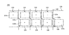
- FIG. 1 illustrates the pixel array of an LCD according to an embodiment of the invention.
- the pixel array 100 comprises pixel electrodes 110 and 115 .
- the pixel electrode 110 comprises two sub-pixel electrodes 110 a and 110 b .
- the sub-pixel electrodes 110 a , 110 b are formed in two neighboring pixel areas 120 sharing an edge and diagonally connected to each other through a connecting part 110 c .
- pixel electrode 115 comprises two sub-pixel electrodes 115 a and 115 b .
- the sub-pixel electrodes 115 a and 115 b are formed in two neighboring pixel areas 120 sharing an edge and diagonally connected to each other through a connecting part 115 c .
- a repeating unit of the pattern formed by the first sub-pixel electrodes 110 a , 110 b and the second sub-pixel electrodes 115 a , 115 b is two first sub-pixel electrodes 110 a , 110 b in the two diagonal areas of a parallelogram and two second sub-pixel electrodes 115 a , 115 b in the other two diagonal areas of the parallelogram.
- Each of the above mentioned pixel area 120 is defined by a pair of scan lines 130 and a pair of data lines 140 .
- a switch device 150 is formed in one corner of the pixel area 120 .
- the switch device 150 of this embodiment is a thin film transistor with a gate, a source and a drain connected to the scan line 130 , the data line 140 , the sub-pixel electrode 110 b or 115 b , respectively.
- the pixel electrodes 110 , 115 shown in FIG. 1 are formed on a switch device substrate alternatively.
- the two neighboring pixel electrodes 110 , 115 can be controlled to have opposite polarities, so that one pixel area 120 comprising two sub-pixel electrodes 110 b , 115 a (or 110 a , 115 b ) with opposite polarities can be obtained.
- the sub-pixel electrodes 110 b , 115 a (or 110 a , 115 b ) in one pixel area 120 belong to two different pixel electrodes 115 , 110 .
- the two sub-pixel electrodes ( 110 a , 110 b ) or ( 115 a , 115 b ) of one pixel electrode 110 or 115 are still connected to each other, only one switch device is required to drive the pixel electrodes 110 , 115 .
- dot inversion method or any appropriate method can be used to allow the two neighboring pixel electrodes 110 , 115 to have opposite polarities.
- FIG. 2 illustrates the pixel array of an LCD according to another embodiment of the invention.
- FIG. 2 shows that pixel array 200 is composed of pixel electrodes 210 and 215 .
- the pixel electrode 210 is divided into three sub-pixel electrodes 210 a , 210 b , and 210 c .
- the sub-pixel electrodes 210 a , 210 b , and 210 c are formed in the two neighboring pixel areas 220 sharing an edge.
- the sub-pixel electrode 210 b is diagonally connected to the sub-pixel electrodes 210 a and 210 c through connecting parts 210 d and 210 e .
- the pixel electrode 215 is divided into three sub-pixel electrodes 215 a , 215 b , and 215 c .
- the sub-pixel electrodes 215 a , 215 b , and 215 c are formed in the two neighboring pixel areas 22 sharing an edge.
- the sub-pixel electrode 215 b is diagonally connected to sub-pixel electrodes 215 a and 215 c through connecting parts 215 d and 215 e .
- a repeating unit of the pattern formed by, for example, the first sub-pixel electrodes 210 a , 110 b and the second sub-pixel electrodes 215 a , 215 b is two first sub-pixel electrodes 210 a , 210 b in the two diagonal areas of a parallelogram and two second sub-pixel electrodes 215 a , 215 b in the other two diagonal areas of the parallelogram.
- Each of the above mentioned pixel area 220 is defined by a pair of scan lines 230 and a pair of data lines 240 .
- a switch device 250 is formed in one corner of each pixel area 220 .
- the switch device 250 in this embodiment is a thin film transistor with a gate, a source and a drain connected to the scan line 230 , the data line 240 and the sub-pixel electrode 210 c or 215 c , respectively.
- the pixel electrodes 210 and 215 are alternatively formed on a switch device substrate.
- the three sub-pixel electrodes 210 a , 215 b , 210 c (or 215 a , 210 b , 215 c ) within the same pixel area 220 have opposite polarities between the sub-pixel electrodes 210 a , 210 c (or 215 a , 215 c ) and the sub-pixel electrode 215 b (or 210 b ) when the neighboring pixel electrode 210 and the pixel electrode 215 have opposite polarities.
- the sub-pixel electrodes 210 a , 210 b 210 c of the pixel electrode 210 are arranged in two pixel areas 220 sharing an edge, the sub-pixel electrodes 210 a , 210 b , 210 c of the pixel electrode 210 are connected through the connecting parts 210 d and 210 e . Hence, only one switch device 250 is required for the pixel electrode 210 .
- the sub-pixel electrodes 215 a , 215 b , 215 c of the pixel electrode 215 are also connected through the connecting parts 215 d and 215 e ; hence only one switch device 250 is required for the pixel electrode 215 .
- the way to obtain two neighboring pixel electrodes 210 , 215 with opposite polarities can be, for example, dot inversion.
- FIG. 3 illustrates the pixel array of an LCD according to another embodiment of the invention.
- the pixel array 300 is composed of pixel electrodes 310 and 315 .
- the pixel electrode 310 is divided into two sub-pixel electrodes 310 a and 310 b located in two pixel areas 320 sharing a corner.
- the sub-pixel electrodes 310 a and 310 b are connected to each other through a connecting part 310 c .
- pixel electrode 315 comprises two sub-pixel electrodes 315 a , 315 b located in two pixel areas 320 sharing a corner.
- the sub-pixel electrodes 315 a and 315 b are connected to each other through a connecting part 315 c .
- a repeating unit of a pattern formed by the first sub-pixel electrodes 310 a , 310 b and the second sub-pixel electrodes 315 a , 315 b is two first sub-pixel electrodes 310 a , 310 b located in the two opposite edges of a parallelogram and two second sub-pixel electrodes 315 a , 315 b located in the other two opposite edges of the parallelogram.
- the above mentioned pixel area 320 is defined by a pair of scan line 330 and a pair of data line 340 .
- a switch device 350 is formed in one corner of the pixel area 320 .
- the switch device 350 in this embodiment is a thin film transistor with a gate, a source and a drain connected to the scan line 330 , the data line 340 , the sub-pixel electrode 310 a or 315 a , respectively.
- the pixel electrodes 310 , 315 shown in FIG. 3 are formed on a switch device substrate alternatively.
- the two neighboring pixel electrodes 310 , 315 can be controlled to have opposite polarities, so that the same pixel area 320 comprising two sub-pixel electrodes 310 b , 315 a (or 315 b , 310 a ) with opposite polarities can be obtained.
- the two sub-pixel electrodes 310 b , 315 a (or 315 b , 310 a ) in one pixel area 320 belong to two different pixel electrodes 315 and 310
- the two sub-pixel electrodes 310 a , 310 b (or 315 a , 315 b ) belonged the pixel electrode 310 (or 315 ) are still connected to each other through the connecting part 310 c .
- only one switch device is required to drive the pixel electrode 310 (or 315 ).
- dot inversion method or any appropriate method can be used to allow the two neighboring pixel electrodes 310 , 315 to have opposite polarities.
- an LCD 400 comprises a lower substrate 410 , an upper substrate 420 and a liquid crystal layer 430 disposed therebetween.
- the upper substrate 420 can be a color filter if the lower substrate 410 is a control circuit board.
- the control circuit board and the color filter layer can be formed on the lower substrate 410 , and there is only a common electrode layer on the upper substrate 420 .
- the structure can be either COA (Color Filter on Array) or AOC (Array on Color Filter).
- COA Color Filter on Array
- AOC Array on Color Filter
- the pixel electrode is only divided into several structurally connected sub-pixel electrodes. Only one driving switch device is required for one pixel. Furthermore, pixel electrodes with opposite polarities are alternatively arranged. At least two sub-pixel electrodes can be formed on each pixel area without additional signal line and driving switch device.
Landscapes
- Physics & Mathematics (AREA)
- Chemical & Material Sciences (AREA)
- Crystallography & Structural Chemistry (AREA)
- Nonlinear Science (AREA)
- General Physics & Mathematics (AREA)
- Engineering & Computer Science (AREA)
- Mathematical Physics (AREA)
- Optics & Photonics (AREA)
- Computer Hardware Design (AREA)
- Theoretical Computer Science (AREA)
- Liquid Crystal (AREA)
Abstract
Description
Claims (9)
Priority Applications (1)
| Application Number | Priority Date | Filing Date | Title |
|---|---|---|---|
| US13/034,747 US8077285B2 (en) | 2006-03-17 | 2011-02-25 | Liquid crystal display including neighboring sub-pixel electrodes with opposite polarities in the same pixel |
Applications Claiming Priority (5)
| Application Number | Priority Date | Filing Date | Title |
|---|---|---|---|
| TW95109332A | 2006-03-17 | ||
| TW095109332A TWI328128B (en) | 2006-03-17 | 2006-03-17 | Liquid crystal display |
| TW95109332 | 2006-03-17 | ||
| US11/684,762 US7924387B2 (en) | 2006-03-17 | 2007-03-12 | Liquid crystal display including neighboring sub-pixel electrodes with opposite polarities in the same pixel |
| US13/034,747 US8077285B2 (en) | 2006-03-17 | 2011-02-25 | Liquid crystal display including neighboring sub-pixel electrodes with opposite polarities in the same pixel |
Related Parent Applications (1)
| Application Number | Title | Priority Date | Filing Date |
|---|---|---|---|
| US11/684,762 Division US7924387B2 (en) | 2006-03-17 | 2007-03-12 | Liquid crystal display including neighboring sub-pixel electrodes with opposite polarities in the same pixel |
Publications (2)
| Publication Number | Publication Date |
|---|---|
| US20110149225A1 US20110149225A1 (en) | 2011-06-23 |
| US8077285B2 true US8077285B2 (en) | 2011-12-13 |
Family
ID=38517245
Family Applications (2)
| Application Number | Title | Priority Date | Filing Date |
|---|---|---|---|
| US11/684,762 Active 2030-02-09 US7924387B2 (en) | 2006-03-17 | 2007-03-12 | Liquid crystal display including neighboring sub-pixel electrodes with opposite polarities in the same pixel |
| US13/034,747 Active US8077285B2 (en) | 2006-03-17 | 2011-02-25 | Liquid crystal display including neighboring sub-pixel electrodes with opposite polarities in the same pixel |
Family Applications Before (1)
| Application Number | Title | Priority Date | Filing Date |
|---|---|---|---|
| US11/684,762 Active 2030-02-09 US7924387B2 (en) | 2006-03-17 | 2007-03-12 | Liquid crystal display including neighboring sub-pixel electrodes with opposite polarities in the same pixel |
Country Status (4)
| Country | Link |
|---|---|
| US (2) | US7924387B2 (en) |
| JP (1) | JP4394114B2 (en) |
| KR (1) | KR100857255B1 (en) |
| TW (1) | TWI328128B (en) |
Cited By (1)
| Publication number | Priority date | Publication date | Assignee | Title |
|---|---|---|---|---|
| US20120007082A1 (en) * | 2010-07-09 | 2012-01-12 | Samsung Electronics Co., Ltd. | Thin film transistor array panel |
Families Citing this family (19)
| Publication number | Priority date | Publication date | Assignee | Title |
|---|---|---|---|---|
| US8107030B2 (en) * | 2005-09-15 | 2012-01-31 | Haip L. Ong | Pixels using associated dot polarity for multi-domain vertical alignment liquid crystal displays |
| US8747879B2 (en) | 2006-04-28 | 2014-06-10 | Advanced Cardiovascular Systems, Inc. | Method of fabricating an implantable medical device to reduce chance of late inflammatory response |
| US9517149B2 (en) | 2004-07-26 | 2016-12-13 | Abbott Cardiovascular Systems Inc. | Biodegradable stent with enhanced fracture toughness |
| US7731890B2 (en) | 2006-06-15 | 2010-06-08 | Advanced Cardiovascular Systems, Inc. | Methods of fabricating stents with enhanced fracture toughness |
| US7971333B2 (en) | 2006-05-30 | 2011-07-05 | Advanced Cardiovascular Systems, Inc. | Manufacturing process for polymetric stents |
| US8253897B2 (en) * | 2005-09-15 | 2012-08-28 | Hiap L. Ong | Spread pixel design for multi domain LCD |
| KR101407285B1 (en) * | 2006-05-22 | 2014-06-13 | 엘지디스플레이 주식회사 | Liquid Crystal Display Device and Method for Driving the Same |
| KR20080053644A (en) * | 2006-12-11 | 2008-06-16 | 삼성전자주식회사 | Liquid crystal display |
| EP2077466A1 (en) * | 2008-01-07 | 2009-07-08 | TPO Displays Corp. | Electrode structure for an LCD device |
| KR100893488B1 (en) * | 2008-02-28 | 2009-04-17 | 삼성모바일디스플레이주식회사 | LCD Display |
| CN102902116B (en) | 2008-05-11 | 2016-02-10 | Nlt科技股份有限公司 | The pel array of non-rectangle and there is the display device of this array |
| CN101644863B (en) * | 2008-08-06 | 2011-08-31 | 北京京东方光电科技有限公司 | TFT-LCD pixel structure and manufacturing method thereof |
| TWI399733B (en) * | 2008-09-19 | 2013-06-21 | Innolux Corp | Liquid crystal display panel, driving method of liquid crystal display panel and liquid crystal display apparatus |
| TW201013621A (en) * | 2008-09-23 | 2010-04-01 | Acer Inc | Liquid crystal display panel and pixel driving device for the liquid crystal display panel |
| CN103713415B (en) * | 2013-12-27 | 2016-10-26 | 合肥京东方光电科技有限公司 | A kind of pixel cell, display device and driving method thereof |
| CN105185288A (en) | 2015-08-28 | 2015-12-23 | 京东方科技集团股份有限公司 | A pixel array, a display driving device and its driving method, and a display device |
| TWI695205B (en) * | 2018-08-10 | 2020-06-01 | 友達光電股份有限公司 | Image-sensing display device and image processing method |
| CN110335563B (en) * | 2018-08-10 | 2022-10-21 | 友达光电股份有限公司 | Display device and operation method thereof |
| CN115755471B (en) * | 2022-11-21 | 2024-03-15 | 厦门天马微电子有限公司 | Display panel and display device |
Citations (11)
| Publication number | Priority date | Publication date | Assignee | Title |
|---|---|---|---|---|
| JPH11119193A (en) | 1997-10-16 | 1999-04-30 | Sony Corp | Liquid crystal display |
| KR20020072723A (en) | 2001-03-12 | 2002-09-18 | 삼성전자 주식회사 | Liquid crystal display device and a driving method thereof |
| TW200428345A (en) | 2003-06-11 | 2004-12-16 | Hannstar Display Corp | LCD panel |
| US20050041188A1 (en) | 2003-08-11 | 2005-02-24 | Seiko Epson Corporation | Pixel structure, electro-optical apparatus, and electronic instrument |
| WO2005040904A1 (en) | 2003-10-29 | 2005-05-06 | Samsung Electronics Co., Ltd. | Liquid crystal display of using dual select diode |
| US20050105032A1 (en) | 2003-11-18 | 2005-05-19 | Hitachi Displays, Ltd. | Liquid crystal display device |
| US6922183B2 (en) | 2002-11-01 | 2005-07-26 | Chin-Lung Ting | Multi-domain vertical alignment liquid crystal display and driving method thereof |
| US6958791B2 (en) | 2002-06-06 | 2005-10-25 | Sharp Kabushiki Kaisha | Liquid crystal display |
| JP2005316211A (en) | 2004-04-30 | 2005-11-10 | Fujitsu Display Technologies Corp | Liquid crystal display device with improved viewing angle characteristics |
| US20070058122A1 (en) * | 2005-09-15 | 2007-03-15 | Kyoritsu Optronics Co., Ltd. | Large pixel multi-domain vertical alignment liquid crystal display using fringe fields |
| US20080002109A1 (en) * | 2005-09-15 | 2008-01-03 | Kyoritsu Optronics Co., Ltd. And Haip L. Ong | Display Unit with Interleaved Pixels |
-
2006
- 2006-03-17 TW TW095109332A patent/TWI328128B/en not_active IP Right Cessation
- 2006-12-20 JP JP2006342605A patent/JP4394114B2/en active Active
-
2007
- 2007-03-12 US US11/684,762 patent/US7924387B2/en active Active
- 2007-03-15 KR KR1020070025531A patent/KR100857255B1/en active Active
-
2011
- 2011-02-25 US US13/034,747 patent/US8077285B2/en active Active
Patent Citations (11)
| Publication number | Priority date | Publication date | Assignee | Title |
|---|---|---|---|---|
| JPH11119193A (en) | 1997-10-16 | 1999-04-30 | Sony Corp | Liquid crystal display |
| KR20020072723A (en) | 2001-03-12 | 2002-09-18 | 삼성전자 주식회사 | Liquid crystal display device and a driving method thereof |
| US6958791B2 (en) | 2002-06-06 | 2005-10-25 | Sharp Kabushiki Kaisha | Liquid crystal display |
| US6922183B2 (en) | 2002-11-01 | 2005-07-26 | Chin-Lung Ting | Multi-domain vertical alignment liquid crystal display and driving method thereof |
| TW200428345A (en) | 2003-06-11 | 2004-12-16 | Hannstar Display Corp | LCD panel |
| US20050041188A1 (en) | 2003-08-11 | 2005-02-24 | Seiko Epson Corporation | Pixel structure, electro-optical apparatus, and electronic instrument |
| WO2005040904A1 (en) | 2003-10-29 | 2005-05-06 | Samsung Electronics Co., Ltd. | Liquid crystal display of using dual select diode |
| US20050105032A1 (en) | 2003-11-18 | 2005-05-19 | Hitachi Displays, Ltd. | Liquid crystal display device |
| JP2005316211A (en) | 2004-04-30 | 2005-11-10 | Fujitsu Display Technologies Corp | Liquid crystal display device with improved viewing angle characteristics |
| US20070058122A1 (en) * | 2005-09-15 | 2007-03-15 | Kyoritsu Optronics Co., Ltd. | Large pixel multi-domain vertical alignment liquid crystal display using fringe fields |
| US20080002109A1 (en) * | 2005-09-15 | 2008-01-03 | Kyoritsu Optronics Co., Ltd. And Haip L. Ong | Display Unit with Interleaved Pixels |
Non-Patent Citations (5)
| Title |
|---|
| Chinese language Notice of Allowance dated Sep. 29, 2009 and its English language translation. |
| English language translation of abstract of JP 11119193 (published Apr. 30, 199). |
| English language translation of abstract of JP 2005316211 (published Nov. 10, 2005). |
| English language translation of abstract of KR 1020020072723 (published Sep. 18, 2002). |
| English language translation of abstract of TW 200428345 (published Dec. 16, 2004). |
Cited By (2)
| Publication number | Priority date | Publication date | Assignee | Title |
|---|---|---|---|---|
| US20120007082A1 (en) * | 2010-07-09 | 2012-01-12 | Samsung Electronics Co., Ltd. | Thin film transistor array panel |
| US8665405B2 (en) * | 2010-07-09 | 2014-03-04 | Samsung Display Co., Ltd. | Thin film transistor array panel |
Also Published As
| Publication number | Publication date |
|---|---|
| JP4394114B2 (en) | 2010-01-06 |
| TW200736701A (en) | 2007-10-01 |
| TWI328128B (en) | 2010-08-01 |
| US20070216619A1 (en) | 2007-09-20 |
| JP2007249178A (en) | 2007-09-27 |
| KR20070094507A (en) | 2007-09-20 |
| US20110149225A1 (en) | 2011-06-23 |
| KR100857255B1 (en) | 2008-09-05 |
| US7924387B2 (en) | 2011-04-12 |
Similar Documents
| Publication | Publication Date | Title |
|---|---|---|
| US8077285B2 (en) | Liquid crystal display including neighboring sub-pixel electrodes with opposite polarities in the same pixel | |
| CN102156367B (en) | Array substrate, liquid crystal panel and liquid crystal displayer | |
| US7663708B2 (en) | Multi-domain liquid crystal display | |
| US8339343B2 (en) | Liquid crystal display device | |
| JPH095766A (en) | Liquid crystal display | |
| JP2005539270A (en) | Liquid crystal display | |
| US9646553B2 (en) | Display device | |
| JPH08179341A (en) | Liquid crystal display device and driving method thereof | |
| US20160274403A1 (en) | Display device | |
| KR101526262B1 (en) | Liquid crystal display devices and electronic devices | |
| CN102692769A (en) | Liquid crystal display panel | |
| US20130120670A1 (en) | Liquid Crystal Display Panel with Multi-domain Pixel Layout | |
| CN109116639B (en) | Liquid crystal display device and driving method thereof | |
| CN111650792A (en) | Array substrate, display panel and display device | |
| KR101189267B1 (en) | A thin film transistor array panel and a liquid crystal display | |
| CN102262322A (en) | Liquid crystal display device and liquid crystal display device substrate | |
| KR101327300B1 (en) | Array substrate and display panel having the same | |
| KR20040061786A (en) | Method for fabricating for an array substrate for In-Plane switching mode LCD | |
| KR19990003282A (en) | Planar drive type substrate for liquid crystal display | |
| KR100529556B1 (en) | Flat panel liquid crystal display | |
| KR100640215B1 (en) | Transverse electric field liquid crystal display device | |
| CN110531557A (en) | Array substrate, liquid crystal display panel and display device | |
| JP4152708B2 (en) | Active matrix substrate, manufacturing method thereof, and liquid crystal display device | |
| CN111240116B (en) | Display panel and display device | |
| CN100437314C (en) | Liquid crystal display and pixel electrode array thereof |
Legal Events
| Date | Code | Title | Description |
|---|---|---|---|
| AS | Assignment |
Owner name: AU OPTRONICS CORPORATION, TAIWAN Free format text: ASSIGNMENT OF ASSIGNORS INTEREST;ASSIGNOR:HUNG, MENG-YI;REEL/FRAME:025862/0167 Effective date: 20070302 |
|
| STCF | Information on status: patent grant |
Free format text: PATENTED CASE |
|
| FPAY | Fee payment |
Year of fee payment: 4 |
|
| MAFP | Maintenance fee payment |
Free format text: PAYMENT OF MAINTENANCE FEE, 8TH YEAR, LARGE ENTITY (ORIGINAL EVENT CODE: M1552); ENTITY STATUS OF PATENT OWNER: LARGE ENTITY Year of fee payment: 8 |
|
| MAFP | Maintenance fee payment |
Free format text: PAYMENT OF MAINTENANCE FEE, 12TH YEAR, LARGE ENTITY (ORIGINAL EVENT CODE: M1553); ENTITY STATUS OF PATENT OWNER: LARGE ENTITY Year of fee payment: 12 |