US8076055B2 - Passivation of multi-layer mirror for extreme ultraviolet lithography - Google Patents
Passivation of multi-layer mirror for extreme ultraviolet lithography Download PDFInfo
- Publication number
- US8076055B2 US8076055B2 US12/692,243 US69224310A US8076055B2 US 8076055 B2 US8076055 B2 US 8076055B2 US 69224310 A US69224310 A US 69224310A US 8076055 B2 US8076055 B2 US 8076055B2
- Authority
- US
- United States
- Prior art keywords
- layer
- mirror
- capping layer
- reflector
- substrate
- Prior art date
- Legal status (The legal status is an assumption and is not a legal conclusion. Google has not performed a legal analysis and makes no representation as to the accuracy of the status listed.)
- Expired - Fee Related, expires
Links
- 238000001900 extreme ultraviolet lithography Methods 0.000 title abstract description 15
- 238000002161 passivation Methods 0.000 title description 3
- 239000000463 material Substances 0.000 claims abstract description 28
- MCMNRKCIXSYSNV-UHFFFAOYSA-N Zirconium dioxide Chemical compound O=[Zr]=O MCMNRKCIXSYSNV-UHFFFAOYSA-N 0.000 claims abstract description 18
- 239000000758 substrate Substances 0.000 claims abstract description 15
- CJNBYAVZURUTKZ-UHFFFAOYSA-N hafnium(IV) oxide Inorganic materials O=[Hf]=O CJNBYAVZURUTKZ-UHFFFAOYSA-N 0.000 claims abstract description 6
- 238000000034 method Methods 0.000 claims description 33
- 239000004065 semiconductor Substances 0.000 claims description 14
- 229920002120 photoresistant polymer Polymers 0.000 claims description 13
- XUIMIQQOPSSXEZ-UHFFFAOYSA-N Silicon Chemical compound [Si] XUIMIQQOPSSXEZ-UHFFFAOYSA-N 0.000 claims description 10
- 229910052710 silicon Inorganic materials 0.000 claims description 10
- 239000010703 silicon Substances 0.000 claims description 10
- ZOKXTWBITQBERF-UHFFFAOYSA-N Molybdenum Chemical compound [Mo] ZOKXTWBITQBERF-UHFFFAOYSA-N 0.000 claims description 8
- 229910052750 molybdenum Inorganic materials 0.000 claims description 8
- 239000011733 molybdenum Substances 0.000 claims description 8
- 230000009467 reduction Effects 0.000 claims description 8
- 230000001590 oxidative effect Effects 0.000 claims description 6
- 238000003384 imaging method Methods 0.000 claims description 5
- 238000001459 lithography Methods 0.000 claims description 4
- 238000000059 patterning Methods 0.000 claims description 3
- 239000011521 glass Substances 0.000 claims description 2
- 239000010410 layer Substances 0.000 claims 23
- 239000002356 single layer Substances 0.000 claims 3
- 230000003647 oxidation Effects 0.000 abstract description 26
- 238000007254 oxidation reaction Methods 0.000 abstract description 26
- QVGXLLKOCUKJST-UHFFFAOYSA-N atomic oxygen Chemical compound [O] QVGXLLKOCUKJST-UHFFFAOYSA-N 0.000 abstract description 12
- 239000001301 oxygen Substances 0.000 abstract description 11
- 229910052760 oxygen Inorganic materials 0.000 abstract description 11
- 238000005546 reactive sputtering Methods 0.000 abstract description 10
- 238000000151 deposition Methods 0.000 abstract description 7
- 230000008021 deposition Effects 0.000 abstract description 7
- PNEYBMLMFCGWSK-UHFFFAOYSA-N aluminium oxide Inorganic materials [O-2].[O-2].[O-2].[Al+3].[Al+3] PNEYBMLMFCGWSK-UHFFFAOYSA-N 0.000 abstract description 5
- 229910052593 corundum Inorganic materials 0.000 abstract description 5
- 210000002381 plasma Anatomy 0.000 abstract description 5
- 229910001845 yogo sapphire Inorganic materials 0.000 abstract description 5
- CBENFWSGALASAD-UHFFFAOYSA-N Ozone Chemical compound [O-][O+]=O CBENFWSGALASAD-UHFFFAOYSA-N 0.000 abstract description 3
- 238000000277 atomic layer chemical vapour deposition Methods 0.000 abstract description 3
- PBCFLUZVCVVTBY-UHFFFAOYSA-N tantalum pentoxide Inorganic materials O=[Ta](=O)O[Ta](=O)=O PBCFLUZVCVVTBY-UHFFFAOYSA-N 0.000 abstract description 3
- 230000008569 process Effects 0.000 description 12
- OKTJSMMVPCPJKN-UHFFFAOYSA-N Carbon Chemical compound [C] OKTJSMMVPCPJKN-UHFFFAOYSA-N 0.000 description 10
- 229910052799 carbon Inorganic materials 0.000 description 10
- 239000007789 gas Substances 0.000 description 7
- 230000005855 radiation Effects 0.000 description 7
- 238000004519 manufacturing process Methods 0.000 description 6
- XLYOFNOQVPJJNP-UHFFFAOYSA-N water Chemical compound O XLYOFNOQVPJJNP-UHFFFAOYSA-N 0.000 description 6
- 238000010521 absorption reaction Methods 0.000 description 4
- 230000004888 barrier function Effects 0.000 description 4
- 238000010494 dissociation reaction Methods 0.000 description 4
- 230000005593 dissociations Effects 0.000 description 4
- 238000009792 diffusion process Methods 0.000 description 3
- 229930195733 hydrocarbon Natural products 0.000 description 3
- 150000002430 hydrocarbons Chemical class 0.000 description 3
- 239000000203 mixture Substances 0.000 description 3
- XKRFYHLGVUSROY-UHFFFAOYSA-N Argon Chemical compound [Ar] XKRFYHLGVUSROY-UHFFFAOYSA-N 0.000 description 2
- IJGRMHOSHXDMSA-UHFFFAOYSA-N Atomic nitrogen Chemical compound N#N IJGRMHOSHXDMSA-UHFFFAOYSA-N 0.000 description 2
- KJTLSVCANCCWHF-UHFFFAOYSA-N Ruthenium Chemical compound [Ru] KJTLSVCANCCWHF-UHFFFAOYSA-N 0.000 description 2
- 230000004075 alteration Effects 0.000 description 2
- XAGFODPZIPBFFR-UHFFFAOYSA-N aluminium Chemical compound [Al] XAGFODPZIPBFFR-UHFFFAOYSA-N 0.000 description 2
- 238000005516 engineering process Methods 0.000 description 2
- 238000005530 etching Methods 0.000 description 2
- 230000003287 optical effect Effects 0.000 description 2
- 229910052707 ruthenium Inorganic materials 0.000 description 2
- 238000004544 sputter deposition Methods 0.000 description 2
- 238000010301 surface-oxidation reaction Methods 0.000 description 2
- 239000004215 Carbon black (E152) Substances 0.000 description 1
- MYMOFIZGZYHOMD-UHFFFAOYSA-N Dioxygen Chemical compound O=O MYMOFIZGZYHOMD-UHFFFAOYSA-N 0.000 description 1
- UFHFLCQGNIYNRP-UHFFFAOYSA-N Hydrogen Chemical compound [H][H] UFHFLCQGNIYNRP-UHFFFAOYSA-N 0.000 description 1
- 239000006094 Zerodur Substances 0.000 description 1
- AZDRQVAHHNSJOQ-UHFFFAOYSA-N alumane Chemical group [AlH3] AZDRQVAHHNSJOQ-UHFFFAOYSA-N 0.000 description 1
- 229910052782 aluminium Inorganic materials 0.000 description 1
- 229910052786 argon Inorganic materials 0.000 description 1
- 238000006243 chemical reaction Methods 0.000 description 1
- 238000000576 coating method Methods 0.000 description 1
- 238000010276 construction Methods 0.000 description 1
- 238000011109 contamination Methods 0.000 description 1
- 230000003247 decreasing effect Effects 0.000 description 1
- 230000001419 dependent effect Effects 0.000 description 1
- 238000003795 desorption Methods 0.000 description 1
- 229910001882 dioxygen Inorganic materials 0.000 description 1
- 238000009501 film coating Methods 0.000 description 1
- 239000001257 hydrogen Substances 0.000 description 1
- 229910052739 hydrogen Inorganic materials 0.000 description 1
- 238000007737 ion beam deposition Methods 0.000 description 1
- 238000001659 ion-beam spectroscopy Methods 0.000 description 1
- 238000010884 ion-beam technique Methods 0.000 description 1
- 150000002500 ions Chemical class 0.000 description 1
- 238000001755 magnetron sputter deposition Methods 0.000 description 1
- 229910052757 nitrogen Inorganic materials 0.000 description 1
- 238000010943 off-gassing Methods 0.000 description 1
- 230000000149 penetrating effect Effects 0.000 description 1
- 230000035515 penetration Effects 0.000 description 1
- 238000000206 photolithography Methods 0.000 description 1
- 238000006303 photolysis reaction Methods 0.000 description 1
- 231100000572 poisoning Toxicity 0.000 description 1
- 230000000607 poisoning effect Effects 0.000 description 1
- 238000002310 reflectometry Methods 0.000 description 1
- 238000005478 sputtering type Methods 0.000 description 1
- 230000003068 static effect Effects 0.000 description 1
- 238000006467 substitution reaction Methods 0.000 description 1
- 230000003746 surface roughness Effects 0.000 description 1
- 239000010409 thin film Substances 0.000 description 1
Images


Classifications
-
- G—PHYSICS
- G03—PHOTOGRAPHY; CINEMATOGRAPHY; ANALOGOUS TECHNIQUES USING WAVES OTHER THAN OPTICAL WAVES; ELECTROGRAPHY; HOLOGRAPHY
- G03F—PHOTOMECHANICAL PRODUCTION OF TEXTURED OR PATTERNED SURFACES, e.g. FOR PRINTING, FOR PROCESSING OF SEMICONDUCTOR DEVICES; MATERIALS THEREFOR; ORIGINALS THEREFOR; APPARATUS SPECIALLY ADAPTED THEREFOR
- G03F7/00—Photomechanical, e.g. photolithographic, production of textured or patterned surfaces, e.g. printing surfaces; Materials therefor, e.g. comprising photoresists; Apparatus specially adapted therefor
- G03F7/70—Microphotolithographic exposure; Apparatus therefor
- G03F7/708—Construction of apparatus, e.g. environment aspects, hygiene aspects or materials
- G03F7/7095—Materials, e.g. materials for housing, stage or other support having particular properties, e.g. weight, strength, conductivity, thermal expansion coefficient
- G03F7/70958—Optical materials or coatings, e.g. with particular transmittance, reflectance or anti-reflection properties
-
- B—PERFORMING OPERATIONS; TRANSPORTING
- B82—NANOTECHNOLOGY
- B82Y—SPECIFIC USES OR APPLICATIONS OF NANOSTRUCTURES; MEASUREMENT OR ANALYSIS OF NANOSTRUCTURES; MANUFACTURE OR TREATMENT OF NANOSTRUCTURES
- B82Y10/00—Nanotechnology for information processing, storage or transmission, e.g. quantum computing or single electron logic
-
- G—PHYSICS
- G03—PHOTOGRAPHY; CINEMATOGRAPHY; ANALOGOUS TECHNIQUES USING WAVES OTHER THAN OPTICAL WAVES; ELECTROGRAPHY; HOLOGRAPHY
- G03F—PHOTOMECHANICAL PRODUCTION OF TEXTURED OR PATTERNED SURFACES, e.g. FOR PRINTING, FOR PROCESSING OF SEMICONDUCTOR DEVICES; MATERIALS THEREFOR; ORIGINALS THEREFOR; APPARATUS SPECIALLY ADAPTED THEREFOR
- G03F7/00—Photomechanical, e.g. photolithographic, production of textured or patterned surfaces, e.g. printing surfaces; Materials therefor, e.g. comprising photoresists; Apparatus specially adapted therefor
- G03F7/70—Microphotolithographic exposure; Apparatus therefor
- G03F7/70216—Mask projection systems
- G03F7/70316—Details of optical elements, e.g. of Bragg reflectors, extreme ultraviolet [EUV] multilayer or bilayer mirrors or diffractive optical elements
-
- G—PHYSICS
- G03—PHOTOGRAPHY; CINEMATOGRAPHY; ANALOGOUS TECHNIQUES USING WAVES OTHER THAN OPTICAL WAVES; ELECTROGRAPHY; HOLOGRAPHY
- G03F—PHOTOMECHANICAL PRODUCTION OF TEXTURED OR PATTERNED SURFACES, e.g. FOR PRINTING, FOR PROCESSING OF SEMICONDUCTOR DEVICES; MATERIALS THEREFOR; ORIGINALS THEREFOR; APPARATUS SPECIALLY ADAPTED THEREFOR
- G03F7/00—Photomechanical, e.g. photolithographic, production of textured or patterned surfaces, e.g. printing surfaces; Materials therefor, e.g. comprising photoresists; Apparatus specially adapted therefor
- G03F7/70—Microphotolithographic exposure; Apparatus therefor
- G03F7/708—Construction of apparatus, e.g. environment aspects, hygiene aspects or materials
- G03F7/70908—Hygiene, e.g. preventing apparatus pollution, mitigating effect of pollution or removing pollutants from apparatus
- G03F7/70916—Pollution mitigation, i.e. mitigating effect of contamination or debris, e.g. foil traps
-
- G—PHYSICS
- G21—NUCLEAR PHYSICS; NUCLEAR ENGINEERING
- G21K—TECHNIQUES FOR HANDLING PARTICLES OR IONISING RADIATION NOT OTHERWISE PROVIDED FOR; IRRADIATION DEVICES; GAMMA RAY OR X-RAY MICROSCOPES
- G21K1/00—Arrangements for handling particles or ionising radiation, e.g. focusing or moderating
- G21K1/06—Arrangements for handling particles or ionising radiation, e.g. focusing or moderating using diffraction, refraction or reflection, e.g. monochromators
- G21K1/062—Devices having a multilayer structure
-
- Y—GENERAL TAGGING OF NEW TECHNOLOGICAL DEVELOPMENTS; GENERAL TAGGING OF CROSS-SECTIONAL TECHNOLOGIES SPANNING OVER SEVERAL SECTIONS OF THE IPC; TECHNICAL SUBJECTS COVERED BY FORMER USPC CROSS-REFERENCE ART COLLECTIONS [XRACs] AND DIGESTS
- Y10—TECHNICAL SUBJECTS COVERED BY FORMER USPC
- Y10T—TECHNICAL SUBJECTS COVERED BY FORMER US CLASSIFICATION
- Y10T428/00—Stock material or miscellaneous articles
- Y10T428/12—All metal or with adjacent metals
- Y10T428/12493—Composite; i.e., plural, adjacent, spatially distinct metal components [e.g., layers, joint, etc.]
- Y10T428/1266—O, S, or organic compound in metal component
- Y10T428/12667—Oxide of transition metal or Al
Definitions
- the present invention relates generally to semiconductor fabrication, and more particularly to EUV lithography.
- photolithography techniques used in the fabrication of semiconductor devices utilize an imaging system that directs radiation onto a mask to form a pattern.
- the pattern is projected onto a semiconductor wafer covered with light-sensitive photoresist.
- the photoresist material may be developed to remove excess photoresist material.
- the remaining photoresist material acts as an etching mask for an etching process used to pattern the underlying semiconductor wafer.
- EUV lithography uses radiation having wavelengths of about 10 to 15 nm located between the soft x-ray and the vacuum ultra-violet (VUV) wavelength range.
- EUVL imaging systems are reflective systems.
- EUV reflective systems which may be used as an illuminator, projection optics, reflective optics, condenser optics, reflective photo masks, or the like, use multi-layer, thin-film coatings known as distributed Bragg reflectors.
- the multi-layer coatings typically comprise 40-70, or more, Mo/Si bi-layers with the bi-layer thickness being about half of the respective EUV wavelength being used.
- the surface of the EUV reflective optics including reflective masks which are also considered to be optical elements frequently become contaminated.
- Surface oxidation and carbon deposits are particularly troublesome and can shorten the useful life of the EUV reflective optics such that the use of EUV reflective optics is not commercially feasible.
- Carbon deposits occur due to the absorption of CH-containing molecules (hydrocarbons) on the optics surface from residual gases in the vacuum environment or absorption of carbon containing molecules (CO, CO 2 ) and subsequent photon- or secondary electron induced dissociation and desorption reactions. Resist outgassing may also lead to carbon deposition on the mirror surfaces through photodissociation or through electron-induced dissociation by photon generated secondary electrons of hydrocarbons.
- Surface oxidation may result from residual water vapor through absorption of water and subsequent photon-induced or secondary electron-induced dissociation of H 2 O where the oxygen remains on the surface and the hydrogen desorbs.
- Carbon contaminates may be removed reversibly by controlled introduction of oxidizing gases such as H 2 O.
- oxidizing gases such as H 2 O.
- the partial pressures of hydrocarbon-containing gases and water vapor pressure must be tightly controlled within a very small process window that prevents oxidation without leaving too much carbon on the surface.
- the process is further complicated because EUV optics in an EUV exposure tool are exposed to different EUV intensities and the process window may be different for each mirror.
- oxidation is enhanced by generation of highly reactive radicals (e.g., O, OH) via dissociation of gas phase molecules by the intense EUV radiation above the mirror surfaces.
- the generation of radicals may be different for different light intensities and, therefore, for different mirrors.
- capping layers of silicon, ruthenium, and layers of silicon and ruthenium modified by adding oxygen and/or nitrogen over the surface of the EUV optics were not oxidation resistant and did not provide an effective barrier layer against diffusion of oxides, e.g., O 2 , O, OH, or the like, such that the capping layers were penetrated by these molecules and/or atoms which then oxidized the multi-layer stack below the capping layer causing changes of the optical constants and the thicknesses of the individual layers.
- a reflective device suitable for use in extreme ultraviolet or soft x-ray applications comprises a substrate having a multi-layer reflector.
- a capping layer is formed over the multi-layer reflector to prevent oxidation.
- the capping layer comprises an inert oxide, such as Al 2 O 3 , HfO 2 , ZrO 2 , Ta 2 O 5 , Y 2 O 3 -stabilized ZrO 2 , or the like.
- a method of forming a reflective device suitable for use in extreme ultraviolet or soft x-ray applications includes forming a capping layer over a multi-layer reflector on a substrate.
- the capping layer may be formed by reactive sputtering in an oxygen environment, by non-reactive sputtering wherein the materials are sputtered directly from the respective oxide targets, by non-reactive sputtering of the metallic layer followed by full or partial oxidation (e.g., by natural oxidation, by oxidation in oxygen-containing plasmas, by oxidation in ozone (O 3 ), or the like), by atomic level deposition (e.g., ALCVD), or the like.
- a method of patterning a semiconductor device utilizes an EUVL system having one or more reflective devices, wherein at least one of the reflective devices have a capping layer formed over a multi-layer reflector.
- the capping layer prevents or reduces the oxidation of the multi-layer reflector during operation.
- FIG. 1 illustrates an EUV optics structure in accordance with an embodiment of the present invention
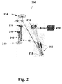
- FIG. 2 illustrates an EUVL system in accordance with an embodiment of the present invention.
- the EUV multi-layer reflector 100 comprises a substrate 110 , a multi-layer reflector 112 , and a capping layer 114 .
- the substrate 110 is formed of a low-thermal expansion material (LTEM) such as ultra-low expansion (ULE) glass available from Corning, Incorporated.
- LTEM low-thermal expansion material
- UEE ultra-low expansion
- other materials such as Zerodur® manufactured by Schott Glass Technologies or the like, may be used.
- the multi-layer reflector 112 comprises alternating layers of a high atomic number Z material and a low atomic number Z material with both materials selected for low absorption index and preferably about 40-70 pairs of alternating layers.
- the high atomic number Z material comprises molybdenum
- the low atomic number Z material comprises silicon.
- the pair of molybdenum and silicon layers is between about 5 and about 7.5 nm (i.e., about half of the EUV wavelength of about 10-15 nm) in thickness.
- the thickness of the multi-layer reflector 112 may be about 200 nm to about 525 nm.
- each pair of alternating molybdenum and silicon layers has a thickness of about 6.8 nm. It should be noted that the preferred thickness is dependent upon the angle of incidence of the EUV radiation on the specific multi-layer reflector. Other thicknesses, materials, and number of layers may be used.
- the capping layer 114 is preferably formed of one or more thin layers of a material that provide good diffusion barrier properties against oxidation of the underlying multi-layer reflector and allow for effective removal of carbon contaminates.
- the capping layer comprises aluminum Al 2 O 3 , about 1 to about 5 nm in thickness, formed by reactive sputtering in an oxygen environment.
- Suitable methods for forming the cap layer include a DC or AC magnetron sputtering or ion beam deposition.
- the former is a diode sputtering method in which magnetic fields at the target (cathode) cause intense local plasma densities and thus high sputter rates.
- ion beams from a separate ion source are obliquely directed to the remote target.
- Reactive sputtering in either method includes sputtering of a metallic target, in the case of Al 2 O 3 this is metallic aluminum.
- Process gases that may be used include argon with an addition of about 10% to about 20% oxygen that reacts with the ejected aluminum atoms from the target surface. It is desirable to have a precise partial pressure control of oxygen to avoid poisoning (oxidation) of the target resulting in large changes of sputter rates.
- Both types of sputtering systems are preferably comprised of single or multi target systems, UHV design, single substrate processing, and dynamic or static deposition modes.
- the substrate is rotated and/or moved along a straight or a curved path (e.g. using a planetary system) to achieve the necessary deposition rate uniformity ( ⁇ 3% (3Sigma).
- Shaper plates may be used to optimize uniformity.
- the Al 2 O 3 capping layer has been found to be fabricated using relatively low process temperatures (less than about 200° C.) and yet provides suitable diffusion barrier properties up to about 700° C., a temperature frequently considered beyond the maximum multi-layer reflector temperatures occurring during fabrication of these reflectors or during operation of the EUV exposure tool.
- inert oxides such as HfO 2 , ZrO 2 , Ta 2 O 5 , Y 2 O 3 -stabilized ZrO 2 , and the like, may also be used.
- Other processes such as non-reactive sputtering wherein the materials are sputtered directly from the respective oxide targets, non-reactive sputtering of the metallic layer followed by full or partial oxidation (e.g., by natural oxidation, by oxidation in oxygen-containing plasmas, by oxidation in ozone (O 3 ), or the like), atomic level deposition (e.g., ALCVD), or the like, may also be used.
- non-reactive sputtering wherein the materials are sputtered directly from the respective oxide targets
- non-reactive sputtering of the metallic layer followed by full or partial oxidation e.g., by natural oxidation, by oxidation in oxygen-containing plasmas, by oxidation in ozone (O 3 ), or the like
- capping layers formed of these materials provide a low surface roughness less than 0.2 nm and a high thickness uniformity in the order of 10 ⁇ 2 to 5 ⁇ 10 ⁇ 2 nm. This creates a highly reflective surface having low aberrations suitable for EUVL technologies and for 50 nm and below designs.
- the low process temperatures used to form the capping layer prevents or reduces the amount of interdiffusion between the layers of the reflector layer.
- a EUV reflector formed in this manner allows carbon contaminates to be removed without the problem of oxidation.
- the carbon contaminates may be removed by introduction of oxidizing gases such as H 2 O.
- oxygen from the introduction of the oxidizing gases remain on the EUV reflector surface (penetrating the capping layer, if any) and oxidizes the Bragg reflectors, thereby decreasing performance characteristics.
- embodiments of the present invention prevent or reduce the penetration of atomic and molecular oxygen, thereby protecting the surface of the Bragg reflectors.
- the capping layer also prevents or reduces the amount of oxidation that may occur on the surface of the capping layer.
- the EUVL system 200 comprises a laser (or other radiation source) 210 , condenser mirrors 212 , a reflective mask 214 , reduction mirrors 216 , and a semiconductor wafer 218 .
- Each of the mirrors may include a mirror having a capping layer fabricated in accordance with an embodiment of the present invention.
- Embodiments of the present invention may be used with other imaging systems and configurations.
- the condenser mirrors 212 collect and focus the radiation generated by the laser 210 onto the reflective mask 214 .
- the reflective mask 214 which is typically scanned, reflects the desired pattern onto the reduction mirrors 216 .
- the reduction mirrors 216 reduce the size of the mask and project the mask having the desired size onto the semiconductor wafer 218 .
- the use of the EUV optics in accordance with an embodiment of the present invention provides a capping layer that provides an oxidation barrier layer that prevents oxidation of the underlying Bragg reflectors, thereby providing better reflectivity and a longer useful life.
Landscapes
- Physics & Mathematics (AREA)
- Engineering & Computer Science (AREA)
- Health & Medical Sciences (AREA)
- Public Health (AREA)
- Epidemiology (AREA)
- General Physics & Mathematics (AREA)
- Life Sciences & Earth Sciences (AREA)
- Atmospheric Sciences (AREA)
- Nanotechnology (AREA)
- Chemical & Material Sciences (AREA)
- Environmental & Geological Engineering (AREA)
- Spectroscopy & Molecular Physics (AREA)
- Mathematical Physics (AREA)
- Theoretical Computer Science (AREA)
- General Engineering & Computer Science (AREA)
- Crystallography & Structural Chemistry (AREA)
- High Energy & Nuclear Physics (AREA)
- Exposure Of Semiconductors, Excluding Electron Or Ion Beam Exposure (AREA)
- Exposure And Positioning Against Photoresist Photosensitive Materials (AREA)
- Optical Elements Other Than Lenses (AREA)
- Preparing Plates And Mask In Photomechanical Process (AREA)
Abstract
Description
Claims (9)
Priority Applications (2)
| Application Number | Priority Date | Filing Date | Title |
|---|---|---|---|
| US12/692,243 US8076055B2 (en) | 2004-07-28 | 2010-01-22 | Passivation of multi-layer mirror for extreme ultraviolet lithography |
| US13/307,589 US8501373B2 (en) | 2004-07-28 | 2011-11-30 | Passivation of multi-layer mirror for extreme ultraviolet lithography |
Applications Claiming Priority (3)
| Application Number | Priority Date | Filing Date | Title |
|---|---|---|---|
| US10/901,627 US20060024589A1 (en) | 2004-07-28 | 2004-07-28 | Passivation of multi-layer mirror for extreme ultraviolet lithography |
| US12/624,263 US7859648B2 (en) | 2004-07-28 | 2009-11-23 | Passivation of multi-layer mirror for extreme ultraviolet lithography |
| US12/692,243 US8076055B2 (en) | 2004-07-28 | 2010-01-22 | Passivation of multi-layer mirror for extreme ultraviolet lithography |
Related Parent Applications (1)
| Application Number | Title | Priority Date | Filing Date |
|---|---|---|---|
| US12/624,263 Division US7859648B2 (en) | 2004-07-28 | 2009-11-23 | Passivation of multi-layer mirror for extreme ultraviolet lithography |
Related Child Applications (1)
| Application Number | Title | Priority Date | Filing Date |
|---|---|---|---|
| US13/307,589 Continuation US8501373B2 (en) | 2004-07-28 | 2011-11-30 | Passivation of multi-layer mirror for extreme ultraviolet lithography |
Publications (2)
| Publication Number | Publication Date |
|---|---|
| US20100119981A1 US20100119981A1 (en) | 2010-05-13 |
| US8076055B2 true US8076055B2 (en) | 2011-12-13 |
Family
ID=35732657
Family Applications (4)
| Application Number | Title | Priority Date | Filing Date |
|---|---|---|---|
| US10/901,627 Abandoned US20060024589A1 (en) | 2004-07-28 | 2004-07-28 | Passivation of multi-layer mirror for extreme ultraviolet lithography |
| US12/624,263 Expired - Fee Related US7859648B2 (en) | 2004-07-28 | 2009-11-23 | Passivation of multi-layer mirror for extreme ultraviolet lithography |
| US12/692,243 Expired - Fee Related US8076055B2 (en) | 2004-07-28 | 2010-01-22 | Passivation of multi-layer mirror for extreme ultraviolet lithography |
| US13/307,589 Expired - Fee Related US8501373B2 (en) | 2004-07-28 | 2011-11-30 | Passivation of multi-layer mirror for extreme ultraviolet lithography |
Family Applications Before (2)
| Application Number | Title | Priority Date | Filing Date |
|---|---|---|---|
| US10/901,627 Abandoned US20060024589A1 (en) | 2004-07-28 | 2004-07-28 | Passivation of multi-layer mirror for extreme ultraviolet lithography |
| US12/624,263 Expired - Fee Related US7859648B2 (en) | 2004-07-28 | 2009-11-23 | Passivation of multi-layer mirror for extreme ultraviolet lithography |
Family Applications After (1)
| Application Number | Title | Priority Date | Filing Date |
|---|---|---|---|
| US13/307,589 Expired - Fee Related US8501373B2 (en) | 2004-07-28 | 2011-11-30 | Passivation of multi-layer mirror for extreme ultraviolet lithography |
Country Status (3)
| Country | Link |
|---|---|
| US (4) | US20060024589A1 (en) |
| CN (1) | CN1737687A (en) |
| DE (1) | DE102005033141A1 (en) |
Families Citing this family (57)
| Publication number | Priority date | Publication date | Assignee | Title |
|---|---|---|---|---|
| US6882406B2 (en) * | 2002-06-14 | 2005-04-19 | Asml Netherlands B.V. | Euv lithographic projection apparatus comprising an optical element with a self-assembled monolayer, optical element with a self-assembled monolayer, method of applying a self-assembled monolayer, device manufacturing method and device manufactured thereby |
| US20060024589A1 (en) * | 2004-07-28 | 2006-02-02 | Siegfried Schwarzl | Passivation of multi-layer mirror for extreme ultraviolet lithography |
| US7504185B2 (en) * | 2005-10-03 | 2009-03-17 | Asahi Glass Company, Limited | Method for depositing multi-layer film of mask blank for EUV lithography and method for producing mask blank for EUV lithography |
| US7959310B2 (en) * | 2006-09-13 | 2011-06-14 | Carl Zeiss Smt Gmbh | Optical arrangement and EUV lithography device with at least one heated optical element, operating methods, and methods for cleaning as well as for providing an optical element |
| US20080266651A1 (en) * | 2007-04-24 | 2008-10-30 | Katsuhiko Murakami | Optical apparatus, multilayer-film reflective mirror, exposure apparatus, and device |
| FI20070991L (en) * | 2007-12-19 | 2009-06-20 | Beneq Oy | Glass product, product use and manufacturing method |
| DE102009032779A1 (en) * | 2009-07-10 | 2011-01-13 | Carl Zeiss Smt Ag | Mirror for the EUV wavelength range, projection objective for microlithography with such a mirror and projection exposure apparatus for microlithography with such a projection objective |
| DE102010006326A1 (en) * | 2010-01-29 | 2011-08-04 | Asml Netherlands B.V. | Arrangement for use in a projection exposure apparatus for microlithography with a reflective optical element |
| DE102010029049B4 (en) | 2010-05-18 | 2014-03-13 | Carl Zeiss Smt Gmbh | Illumination optics for a metrology system for the examination of an object with EUV illumination light and metrology system with such illumination optics |
| CN102253585A (en) * | 2010-05-20 | 2011-11-23 | 鸿富锦精密工业(深圳)有限公司 | Projection screen and system and manufacture method of projection screen |
| EP2729844B1 (en) * | 2011-07-08 | 2021-07-28 | ASML Netherlands B.V. | Lithographic patterning process and resists to use therein |
| DE102012202850A1 (en) * | 2012-02-24 | 2013-08-29 | Asml Netherlands B.V. | Method for optimizing a protective layer system for an optical element, optical element and optical system for EUV lithography |
| DE102012207125A1 (en) | 2012-04-27 | 2013-03-28 | Carl Zeiss Smt Gmbh | Optical element comprises extreme-ultraviolet radiation layer, reflecting multilayer system, guard layer system, and upper layer containing chemical compound including three or more different chemical elements |
| US10185234B2 (en) * | 2012-10-04 | 2019-01-22 | Asml Netherlands B.V. | Harsh environment optical element protection |
| US9632411B2 (en) | 2013-03-14 | 2017-04-25 | Applied Materials, Inc. | Vapor deposition deposited photoresist, and manufacturing and lithography systems therefor |
| US20140272684A1 (en) | 2013-03-12 | 2014-09-18 | Applied Materials, Inc. | Extreme ultraviolet lithography mask blank manufacturing system and method of operation therefor |
| US9354508B2 (en) | 2013-03-12 | 2016-05-31 | Applied Materials, Inc. | Planarized extreme ultraviolet lithography blank, and manufacturing and lithography systems therefor |
| US9206078B2 (en) * | 2013-03-13 | 2015-12-08 | Intermolecular, Inc. | Barrier layers for silver reflective coatings and HPC workflows for rapid screening of materials for such barrier layers |
| KR102109129B1 (en) * | 2013-07-02 | 2020-05-08 | 삼성전자주식회사 | Reflective photomask blank and reflective photomask |
| EP2905637A1 (en) * | 2014-02-07 | 2015-08-12 | ASML Netherlands B.V. | EUV optical element having blister-resistant multilayer cap |
| EP3166902A4 (en) * | 2014-07-07 | 2018-01-24 | Scint-X AB | Production of a thin film reflector |
| US9690016B2 (en) * | 2014-07-11 | 2017-06-27 | Applied Materials, Inc. | Extreme ultraviolet reflective element with amorphous layers and method of manufacturing thereof |
| US9581890B2 (en) | 2014-07-11 | 2017-02-28 | Applied Materials, Inc. | Extreme ultraviolet reflective element with multilayer stack and method of manufacturing thereof |
| US9739913B2 (en) * | 2014-07-11 | 2017-08-22 | Applied Materials, Inc. | Extreme ultraviolet capping layer and method of manufacturing and lithography thereof |
| DE102014218084A1 (en) | 2014-09-10 | 2014-11-13 | Carl Zeiss Smt Gmbh | METHOD FOR PRODUCING OXID BASED COATING LAYERS FOR HIGH - REFLECTING EUV MULTILAYERS |
| DE102016208987A1 (en) | 2016-05-24 | 2017-11-30 | Carl Zeiss Smt Gmbh | Optical element and EUV lithography system |
| TWI811037B (en) | 2016-07-27 | 2023-08-01 | 美商應用材料股份有限公司 | Extreme ultraviolet mask blank with multilayer absorber and method of manufacture |
| US10928569B2 (en) * | 2018-04-24 | 2021-02-23 | Palo Alto Research Center Incorporated | Angle-insensitive multi-wavelength optical filters with hue control |
| TW202026770A (en) | 2018-10-26 | 2020-07-16 | 美商應用材料股份有限公司 | Ta-cu alloy material for extreme ultraviolet mask absorber |
| TWI845579B (en) | 2018-12-21 | 2024-06-21 | 美商應用材料股份有限公司 | Extreme ultraviolet mask absorber and processes for manufacture |
| TWI828843B (en) | 2019-01-31 | 2024-01-11 | 美商應用材料股份有限公司 | Extreme ultraviolet (euv) mask blanks and methods of manufacturing the same |
| US11249390B2 (en) | 2019-01-31 | 2022-02-15 | Applied Materials, Inc. | Extreme ultraviolet mask absorber materials |
| TW202035792A (en) | 2019-01-31 | 2020-10-01 | 美商應用材料股份有限公司 | Extreme ultraviolet mask absorber materials |
| TWI842830B (en) | 2019-03-01 | 2024-05-21 | 美商應用材料股份有限公司 | Physical vapor deposition chamber and method of depositing alternating material layers |
| TWI818151B (en) | 2019-03-01 | 2023-10-11 | 美商應用材料股份有限公司 | Physical vapor deposition chamber and method of operation thereof |
| TWI870386B (en) | 2019-03-01 | 2025-01-21 | 美商應用材料股份有限公司 | Euv mask blank and the method making the same |
| TWI836073B (en) | 2019-05-22 | 2024-03-21 | 美商應用材料股份有限公司 | Extreme ultraviolet (euv) mask blank and method of manufacturing the same |
| TWI845677B (en) | 2019-05-22 | 2024-06-21 | 美商應用材料股份有限公司 | Extreme ultraviolet mask absorber materials |
| TW202104667A (en) | 2019-05-22 | 2021-02-01 | 美商應用材料股份有限公司 | Extreme ultraviolet mask absorber materials |
| TWI836072B (en) | 2019-05-22 | 2024-03-21 | 美商應用材料股份有限公司 | Extreme ultraviolet mask with embedded absorber layer |
| TW202104666A (en) | 2019-05-22 | 2021-02-01 | 美商應用材料股份有限公司 | Extreme ultraviolet mask absorber materials |
| CN114127633A (en) * | 2019-07-16 | 2022-03-01 | Asml荷兰有限公司 | Oxygen loss resistant top coat for optical elements |
| US11385536B2 (en) | 2019-08-08 | 2022-07-12 | Applied Materials, Inc. | EUV mask blanks and methods of manufacture |
| US11630385B2 (en) | 2020-01-24 | 2023-04-18 | Applied Materials, Inc. | Extreme ultraviolet mask absorber materials |
| TWI817073B (en) | 2020-01-27 | 2023-10-01 | 美商應用材料股份有限公司 | Extreme ultraviolet mask blank hard mask materials |
| TW202129401A (en) | 2020-01-27 | 2021-08-01 | 美商應用材料股份有限公司 | Extreme ultraviolet mask blank hard mask materials |
| TW202131087A (en) | 2020-01-27 | 2021-08-16 | 美商應用材料股份有限公司 | Extreme ultraviolet mask absorber materials |
| TW202141165A (en) | 2020-03-27 | 2021-11-01 | 美商應用材料股份有限公司 | Extreme ultraviolet mask absorber materials |
| TWI836207B (en) | 2020-04-17 | 2024-03-21 | 美商應用材料股份有限公司 | Extreme ultraviolet mask absorber materials |
| US11300871B2 (en) | 2020-04-29 | 2022-04-12 | Applied Materials, Inc. | Extreme ultraviolet mask absorber materials |
| TW202202641A (en) | 2020-07-13 | 2022-01-16 | 美商應用材料股份有限公司 | Extreme ultraviolet mask absorber materials |
| DE102020212353A1 (en) * | 2020-09-30 | 2022-03-31 | Carl Zeiss Smt Gmbh | Process for producing an optical element, optical element, device for producing an optical element, secondary gas and projection exposure system |
| US11609490B2 (en) | 2020-10-06 | 2023-03-21 | Applied Materials, Inc. | Extreme ultraviolet mask absorber materials |
| US11513437B2 (en) | 2021-01-11 | 2022-11-29 | Applied Materials, Inc. | Extreme ultraviolet mask absorber materials |
| US11592738B2 (en) | 2021-01-28 | 2023-02-28 | Applied Materials, Inc. | Extreme ultraviolet mask absorber materials |
| US11815803B2 (en) | 2021-08-30 | 2023-11-14 | Applied Materials, Inc. | Multilayer extreme ultraviolet reflector materials |
| US11782337B2 (en) | 2021-09-09 | 2023-10-10 | Applied Materials, Inc. | Multilayer extreme ultraviolet reflectors |
Citations (14)
| Publication number | Priority date | Publication date | Assignee | Title |
|---|---|---|---|---|
| US5958605A (en) | 1997-11-10 | 1999-09-28 | Regents Of The University Of California | Passivating overcoat bilayer for multilayer reflective coatings for extreme ultraviolet lithography |
| CN1292431A (en) | 1999-10-06 | 2001-04-25 | 三星电子株式会社 | Method for forming film by using atomic layer deposition method |
| US6228512B1 (en) | 1999-05-26 | 2001-05-08 | The Regents Of The University Of California | MoRu/Be multilayers for extreme ultraviolet applications |
| US6290180B1 (en) | 1999-09-09 | 2001-09-18 | Lockheed Martin Corporation | Photocatalytic coatings on optical solar reflectors to decompose organic contaminants |
| EP1150139A2 (en) | 2000-03-31 | 2001-10-31 | Carl Zeiss | Multilayer system with protecting layer system and production method |
| WO2003032329A1 (en) | 2001-10-04 | 2003-04-17 | Carl Zeiss Smt Ag | Optical element and method for its manufacture as well as lightography apparatus and method for manufacturing a semiconductor device |
| US20030147058A1 (en) | 2002-02-01 | 2003-08-07 | Nikon Corporation | Self-cleaning reflective optical elements for use in X-ray optical systems, and optical systems and microlithography systems comprising same |
| US6627362B2 (en) | 2001-10-30 | 2003-09-30 | Intel Corporation | Photolithographic mask fabrication |
| EP1394815A1 (en) | 2002-08-28 | 2004-03-03 | ASML Netherlands B.V. | Lithographic apparatus comprising a Mo/Si-multilayer with capping layer |
| US6753946B2 (en) | 2001-12-28 | 2004-06-22 | Asml Netherlands B.V. | Lithographic apparatus and device manufacturing method |
| WO2004053540A1 (en) | 2002-12-12 | 2004-06-24 | Carl Zeiss Smt Ag | Protective coating system for reflective optical elements, reflective optical element and methods for the production thereof |
| US6759141B2 (en) | 2002-04-30 | 2004-07-06 | The Regents Of The University Of California | Oxidation preventative capping layer for deep-ultra-violet and soft x-ray multilayers |
| US7078134B2 (en) | 2002-05-21 | 2006-07-18 | Infineon Technologies Ag | Photolithographic mask having a structure region covered by a thin protective coating of only a few atomic layers and methods for the fabrication of the mask including ALCVD to form the thin protective coating |
| US7859648B2 (en) * | 2004-07-28 | 2010-12-28 | Infineon Technologies Ag | Passivation of multi-layer mirror for extreme ultraviolet lithography |
Family Cites Families (2)
| Publication number | Priority date | Publication date | Assignee | Title |
|---|---|---|---|---|
| TW561279B (en) * | 1999-07-02 | 2003-11-11 | Asml Netherlands Bv | Reflector for reflecting radiation in a desired wavelength range, lithographic projection apparatus containing the same and method for their preparation |
| US7567379B2 (en) * | 2004-04-29 | 2009-07-28 | Intel Corporation | Technique to prevent tin contamination of mirrors and electrodes in an EUV lithography system |
-
2004
- 2004-07-28 US US10/901,627 patent/US20060024589A1/en not_active Abandoned
-
2005
- 2005-07-15 DE DE102005033141A patent/DE102005033141A1/en not_active Ceased
- 2005-07-28 CN CN200510087957.5A patent/CN1737687A/en active Pending
-
2009
- 2009-11-23 US US12/624,263 patent/US7859648B2/en not_active Expired - Fee Related
-
2010
- 2010-01-22 US US12/692,243 patent/US8076055B2/en not_active Expired - Fee Related
-
2011
- 2011-11-30 US US13/307,589 patent/US8501373B2/en not_active Expired - Fee Related
Patent Citations (19)
| Publication number | Priority date | Publication date | Assignee | Title |
|---|---|---|---|---|
| US5958605A (en) | 1997-11-10 | 1999-09-28 | Regents Of The University Of California | Passivating overcoat bilayer for multilayer reflective coatings for extreme ultraviolet lithography |
| US6228512B1 (en) | 1999-05-26 | 2001-05-08 | The Regents Of The University Of California | MoRu/Be multilayers for extreme ultraviolet applications |
| US6290180B1 (en) | 1999-09-09 | 2001-09-18 | Lockheed Martin Corporation | Photocatalytic coatings on optical solar reflectors to decompose organic contaminants |
| CN1292431A (en) | 1999-10-06 | 2001-04-25 | 三星电子株式会社 | Method for forming film by using atomic layer deposition method |
| GB2355727A (en) | 1999-10-06 | 2001-05-02 | Samsung Electronics Co Ltd | Atomic layer deposition method |
| US6656575B2 (en) | 2000-03-31 | 2003-12-02 | Carl-Zeiss-Stiftung | Multilayer system with protecting layer system and production method |
| EP1150139A2 (en) | 2000-03-31 | 2001-10-31 | Carl Zeiss | Multilayer system with protecting layer system and production method |
| WO2003032329A1 (en) | 2001-10-04 | 2003-04-17 | Carl Zeiss Smt Ag | Optical element and method for its manufacture as well as lightography apparatus and method for manufacturing a semiconductor device |
| US7172788B2 (en) | 2001-10-04 | 2007-02-06 | Carl Zeiss Smt Ag | Optical element and method for its manufacture as well as lithography apparatus and method for manufacturing a semiconductor device |
| US6627362B2 (en) | 2001-10-30 | 2003-09-30 | Intel Corporation | Photolithographic mask fabrication |
| US6753946B2 (en) | 2001-12-28 | 2004-06-22 | Asml Netherlands B.V. | Lithographic apparatus and device manufacturing method |
| US20030147058A1 (en) | 2002-02-01 | 2003-08-07 | Nikon Corporation | Self-cleaning reflective optical elements for use in X-ray optical systems, and optical systems and microlithography systems comprising same |
| US6759141B2 (en) | 2002-04-30 | 2004-07-06 | The Regents Of The University Of California | Oxidation preventative capping layer for deep-ultra-violet and soft x-ray multilayers |
| US7078134B2 (en) | 2002-05-21 | 2006-07-18 | Infineon Technologies Ag | Photolithographic mask having a structure region covered by a thin protective coating of only a few atomic layers and methods for the fabrication of the mask including ALCVD to form the thin protective coating |
| EP1394815A1 (en) | 2002-08-28 | 2004-03-03 | ASML Netherlands B.V. | Lithographic apparatus comprising a Mo/Si-multilayer with capping layer |
| WO2004053540A1 (en) | 2002-12-12 | 2004-06-24 | Carl Zeiss Smt Ag | Protective coating system for reflective optical elements, reflective optical element and methods for the production thereof |
| DE10258709A1 (en) | 2002-12-12 | 2004-07-01 | Carl Zeiss Smt Ag | Protection system for reflective optical elements, reflective optical element and method for their production |
| US20050276988A1 (en) | 2002-12-12 | 2005-12-15 | Johann Trenkler | Protective coating system for reflective optical elements, reflective optical element and method for the production thereof |
| US7859648B2 (en) * | 2004-07-28 | 2010-12-28 | Infineon Technologies Ag | Passivation of multi-layer mirror for extreme ultraviolet lithography |
Non-Patent Citations (7)
| Title |
|---|
| Braun, A., "ALD Breaks Materials, Conformality Barriers," Semiconductor International (Oct. 2001) pp. 52-54, 56 and 59. |
| Dietze, W., et al., "Landolt-Börnstein: Numerical Data and Functional Relationships in Science and Technology," New Series, vol. 17, Springer-Verlag Berlin, (1984) pp. 308-316. |
| He, Y., et al., "Development of Refractory Silicate-Yttria-Stabilized Zirconia Dual-Layer Thermal Barrier Coatings," Journal of Thermal Spray Technology, vol. 9(1), (Mar. 2000) pp. 59-67. |
| Lee, K.-I, et al., "Characteristics of the Aluminum Thin Films for the Prevention of Copper Oxidation," J. of the Korean Inst. of Telematics and Electronics, vol. 31A, No. 10 (1994) pp. 108-113, (English abstract). |
| Meiling, H., et al., "Progress of the EUVL Alpha Tool," Proceedings of SPIE, vol. 4343 (2001) pp. 38-50. |
| Tichenor, D. A., et al., "System Integration and Performance of the EUV Engineering Test Stand,"Proceedings of SPIE, vol. 4343 (2001) pp. 19-37. |
| Zalar, A., et al., "Interfacial Reactions in Al2O3/Ti, Al2O3/Ti3Al and Al2O3/TiAl Bilayers," Thin Solid Films, vol. 352 (1999) pp. 151-155. |
Also Published As
| Publication number | Publication date |
|---|---|
| CN1737687A (en) | 2006-02-22 |
| US8501373B2 (en) | 2013-08-06 |
| US20060024589A1 (en) | 2006-02-02 |
| US7859648B2 (en) | 2010-12-28 |
| US20100066991A1 (en) | 2010-03-18 |
| DE102005033141A1 (en) | 2006-03-23 |
| US20100119981A1 (en) | 2010-05-13 |
| US20120069311A1 (en) | 2012-03-22 |
Similar Documents
| Publication | Publication Date | Title |
|---|---|---|
| US8076055B2 (en) | Passivation of multi-layer mirror for extreme ultraviolet lithography | |
| US20030147058A1 (en) | Self-cleaning reflective optical elements for use in X-ray optical systems, and optical systems and microlithography systems comprising same | |
| EP2710415B1 (en) | Reflective optical element and optical system for euv lithography | |
| EP1373978B1 (en) | Extreme ultraviolet mask with improved absorber | |
| JP7198936B2 (en) | Extreme UV mask absorber material | |
| JP5568098B2 (en) | Multilayer mirror and lithographic apparatus | |
| US20040231971A1 (en) | Photo mask blank, photo mask, method and apparatus for manufacturing of a photo mask blank | |
| US11988953B2 (en) | EUV masks to prevent carbon contamination | |
| JP2023545014A (en) | Extreme UV mask absorber material | |
| JP2024517210A (en) | Extreme UV mask absorber material | |
| US9046780B2 (en) | Multilayer mirror and lithographic apparatus | |
| KR101625934B1 (en) | Multilayer mirror and lithographic apparatus | |
| Bajt et al. | Design and performance of capping layers for EUV multilayer mirrors | |
| US20220179329A1 (en) | Optical element and euv lithographic system | |
| JP2004153279A (en) | Lithographic apparatus and device manufacturing method | |
| JP2003227898A (en) | Multilayer film reflecting mirror, soft X-ray optical equipment, exposure apparatus and cleaning method thereof | |
| JP2005332972A (en) | OPTICAL ELEMENT, OPTICAL DEVICE, AND SEMICONDUCTOR DEVICE MANUFACTURING METHOD | |
| JP2004172272A (en) | EUV exposure apparatus and EUV exposure method | |
| US20030064161A1 (en) | Method for reducing carbon contamination of multilayer mirrors | |
| CN115485616A (en) | Far-UV mask absorbing material | |
| US20080203386A1 (en) | Method of forming a patterned resist layer for patterning a semiconductor product | |
| KR20090102547A (en) | Method for removing defects | |
| Aoki et al. | Apparatus for contamination control development in EUVA | |
| JP2006170812A (en) | Multilayer reflector, EUV exposure apparatus, and soft X-ray optical instrument | |
| JP2006170813A (en) | Multilayer reflector, EUV exposure apparatus, and soft X-ray optical instrument |
Legal Events
| Date | Code | Title | Description |
|---|---|---|---|
| FEPP | Fee payment procedure |
Free format text: PAYOR NUMBER ASSIGNED (ORIGINAL EVENT CODE: ASPN); ENTITY STATUS OF PATENT OWNER: LARGE ENTITY |
|
| ZAAA | Notice of allowance and fees due |
Free format text: ORIGINAL CODE: NOA |
|
| ZAAB | Notice of allowance mailed |
Free format text: ORIGINAL CODE: MN/=. |
|
| STCF | Information on status: patent grant |
Free format text: PATENTED CASE |
|
| FPAY | Fee payment |
Year of fee payment: 4 |
|
| MAFP | Maintenance fee payment |
Free format text: PAYMENT OF MAINTENANCE FEE, 8TH YEAR, LARGE ENTITY (ORIGINAL EVENT CODE: M1552); ENTITY STATUS OF PATENT OWNER: LARGE ENTITY Year of fee payment: 8 |
|
| FEPP | Fee payment procedure |
Free format text: MAINTENANCE FEE REMINDER MAILED (ORIGINAL EVENT CODE: REM.); ENTITY STATUS OF PATENT OWNER: LARGE ENTITY |
|
| LAPS | Lapse for failure to pay maintenance fees |
Free format text: PATENT EXPIRED FOR FAILURE TO PAY MAINTENANCE FEES (ORIGINAL EVENT CODE: EXP.); ENTITY STATUS OF PATENT OWNER: LARGE ENTITY |
|
| STCH | Information on status: patent discontinuation |
Free format text: PATENT EXPIRED DUE TO NONPAYMENT OF MAINTENANCE FEES UNDER 37 CFR 1.362 |
|
| FP | Lapsed due to failure to pay maintenance fee |
Effective date: 20231213 |