US8074052B2 - System and method for assigning tags to control instruction processing in a superscalar processor - Google Patents
System and method for assigning tags to control instruction processing in a superscalar processor Download PDFInfo
- Publication number
- US8074052B2 US8074052B2 US12/210,738 US21073808A US8074052B2 US 8074052 B2 US8074052 B2 US 8074052B2 US 21073808 A US21073808 A US 21073808A US 8074052 B2 US8074052 B2 US 8074052B2
- Authority
- US
- United States
- Prior art keywords
- instruction
- storage medium
- queue
- instructions
- tag
- Prior art date
- Legal status (The legal status is an assumption and is not a legal conclusion. Google has not performed a legal analysis and makes no representation as to the accuracy of the status listed.)
- Expired - Fee Related, expires
Links
- 238000000034 method Methods 0.000 title description 11
- 238000013461 design Methods 0.000 claims description 17
- 230000003542 behavioural effect Effects 0.000 claims description 13
- 238000004064 recycling Methods 0.000 claims description 13
- 238000012544 monitoring process Methods 0.000 abstract description 6
- 238000010586 diagram Methods 0.000 description 9
- 230000008901 benefit Effects 0.000 description 3
- 230000008859 change Effects 0.000 description 2
- 230000008569 process Effects 0.000 description 2
- 238000012546 transfer Methods 0.000 description 2
- 230000015572 biosynthetic process Effects 0.000 description 1
- 230000000694 effects Effects 0.000 description 1
- 230000006870 function Effects 0.000 description 1
- 238000002955 isolation Methods 0.000 description 1
- 238000012986 modification Methods 0.000 description 1
- 230000004048 modification Effects 0.000 description 1
- 229910052710 silicon Inorganic materials 0.000 description 1
- 239000010703 silicon Substances 0.000 description 1
- 238000003786 synthesis reaction Methods 0.000 description 1
Images


Classifications
-
- G—PHYSICS
- G06—COMPUTING; CALCULATING OR COUNTING
- G06F—ELECTRIC DIGITAL DATA PROCESSING
- G06F9/00—Arrangements for program control, e.g. control units
- G06F9/06—Arrangements for program control, e.g. control units using stored programs, i.e. using an internal store of processing equipment to receive or retain programs
- G06F9/30—Arrangements for executing machine instructions, e.g. instruction decode
- G06F9/38—Concurrent instruction execution, e.g. pipeline or look ahead
- G06F9/3854—Instruction completion, e.g. retiring, committing or graduating
- G06F9/3856—Reordering of instructions, e.g. using queues or age tags
-
- G—PHYSICS
- G06—COMPUTING; CALCULATING OR COUNTING
- G06F—ELECTRIC DIGITAL DATA PROCESSING
- G06F9/00—Arrangements for program control, e.g. control units
- G06F9/06—Arrangements for program control, e.g. control units using stored programs, i.e. using an internal store of processing equipment to receive or retain programs
- G06F9/30—Arrangements for executing machine instructions, e.g. instruction decode
- G06F9/38—Concurrent instruction execution, e.g. pipeline or look ahead
- G06F9/3836—Instruction issuing, e.g. dynamic instruction scheduling or out of order instruction execution
- G06F9/3838—Dependency mechanisms, e.g. register scoreboarding
-
- G—PHYSICS
- G06—COMPUTING; CALCULATING OR COUNTING
- G06F—ELECTRIC DIGITAL DATA PROCESSING
- G06F9/00—Arrangements for program control, e.g. control units
- G06F9/06—Arrangements for program control, e.g. control units using stored programs, i.e. using an internal store of processing equipment to receive or retain programs
- G06F9/30—Arrangements for executing machine instructions, e.g. instruction decode
- G06F9/38—Concurrent instruction execution, e.g. pipeline or look ahead
- G06F9/3854—Instruction completion, e.g. retiring, committing or graduating
- G06F9/3858—Result writeback, i.e. updating the architectural state or memory
-
- G—PHYSICS
- G06—COMPUTING; CALCULATING OR COUNTING
- G06F—ELECTRIC DIGITAL DATA PROCESSING
- G06F9/00—Arrangements for program control, e.g. control units
- G06F9/06—Arrangements for program control, e.g. control units using stored programs, i.e. using an internal store of processing equipment to receive or retain programs
- G06F9/30—Arrangements for executing machine instructions, e.g. instruction decode
- G06F9/38—Concurrent instruction execution, e.g. pipeline or look ahead
- G06F9/3885—Concurrent instruction execution, e.g. pipeline or look ahead using a plurality of independent parallel functional units
Definitions
- the present invention relates generally to superscalar computers, and more particularly, a system and method for using tags to control instruction execution in a superscalar reduced instruction set computer (RISC).
- RISC superscalar reduced instruction set computer
- Processors used in conventional computer systems typically execute program instructions one at a time, in sequential order.
- the process of executing a single instruction involves several sequential steps.
- the first step generally involves fetching the instruction from a memory device.
- the second step generally involves decoding the instruction, and assembling any operands.
- the third step generally involves executing the instruction, and storing the results.
- Some processors are designed to perform each step in a single cycle of the processor clock. Alternatively, the processor may be designed so that the number of processor clock cycles per step depends on the particular instruction.
- Pipelining involves the overlapping of the sequential steps of the execution process. For example, while the processor is performing the execution step for one instruction, it might simultaneously perform the decode step for a second instruction, and perform a fetch of a third instruction. Pipelining can thus decrease the execution time for a sequence of instructions.
- processors improve performance by overlapping the sub-steps of the three sequential steps discussed above are called superpipelined processors.
- Still another technique for improving performance involves executing multiple instructions simultaneously.
- Processors which utilize this technique are generally referred to as superscalar processors.
- the ability of a superscalar processor to execute two or more instructions simultaneously depends on the particular instructions being executed. For example, two instructions which both require use of the same, limited processor resource (such as the floating point unit) cannot be executed simultaneously. This type of conflict is known as a resource dependency.
- an instruction which uses the result produced by the execution of another instruction cannot be executed at the same time as the other instruction.
- An instruction which depends on the result of another instruction is said to have a data dependency on the other instruction.
- an instruction set may specify that particular types of instructions must execute in a certain order relative to each other. These instructions are said to have procedural dependencies.
- a third technique for improving performance involves executing instructions out of program order.
- Processors which utilize this technique are generally referred to as out-of-order processors.
- out-of-order processors are also superscalar processors.
- Data dependencies and procedural dependencies limit out-of-order execution in the same way that they limit superscalar execution.
- the term “superscalar processor” will be used to refer to a processor that is: capable of executing multiple instructions simultaneously, or capable of executing instructions out of program order, or capable of doing both.
- a superscalar processor For executing instructions either simultaneously or out of order, a superscalar processor must contain a system called an Execution unit.
- the Execution Unit contains multiple functional units for executing instructions (e.g., floating point multiplier, adder, etc.). Scheduling control is needed to dispatch instructions to the multiple functional units.
- the processor stops decoding instructions whenever a decoded instruction creates a resource conflict or has a true dependency or an output dependency on a uncompleted instruction. As a result, the processor is not able to look ahead beyond the instructions with the conflict or dependency, even though one or more subsequent instructions might be executable.
- processors isolate the decoder from the execution stage, so that it continues to decode instructions regardless of whether they can be executed immediately. This isolation is accomplished by a buffer between the decode and execute stages, called an instruction window.
- the processor decodes instructions and places them into the window as long as there is room in the window and, at the same time, examines instructions in the window to find instructions that can be executed (that is, instructions that do not have resource conflicts or dependencies).
- the instruction window serves as a pool of instructions, giving the processor lookahead ability that is constrained only by the size of the window and the capability of the instruction source.
- out-of-order issue requires a buffer, called an instruction window between the decoder and functional units; and the instruction window provides a snap-shot of a piece of the program that the computer is executing.
- the new instructions enter the window and completed instructions leave the window in groups of various sizes.
- an instruction window might contain eight instructions (I 0 -I 7 ) and may be changed in groups of one, two or three. In this case, after any of instructions I 0 , I 1 or I 2 have executed, they can be removed from the window and new instructions can be advanced into the window. Instruction windows where instructions enter and leave in groups of various sizes are called “Variable Advance Instruction Windows.”
- VAIW Variable Advance Instruction Windows
- FAIW Fixed Advance Instruction Windows
- fixed advance instruction windows are easier for a processor to manage since a particular instruction can only occupy a fixed number of locations in the window. For example, in an instruction window that contains eight instructions (I 0 -I 7 ) and where instructions can be added or removed in groups of four, an instruction can occupy only one of two locations in the window (e.g., I 0 and I 4 ). In a variable advance instruction windows, that instruction could occupy all of the locations in the window at different times, thus a processor that has a variable advance instruction window must have more resources to track each instruction's position than a processor that has a fixed advance instruction window.
- the present invention is directed to a technique for monitoring instruction execution of multiple instructions in parallel and out of program order using a system that assigns tags to the multiple instructions and maintains an instruction window that contains the multiple instructions.
- the system is a component of a superscalar unit which is coupled between a source of instructions and functional units which execute the instructions.
- the superscalar unit is in charge of maintaining the instruction window, directing instructions to the various functional units in the execution unit, and, after the instructions are executed, receiving new instructions from the source.
- the present invention employs a tag monitor system, which is a part of the superscalar unit.
- the tag monitor system includes: a register file and a queue that operates on a First-In-First-Out basis (the queue is a multiple-advance, multiple output, recycling FIFO).
- the queue is coupled to the register file.
- the register file is coupled to the instruction source and is used to store instruction information (i.e., the resource requirements of each instruction).
- instruction information is then stored in the register file at an address location indicated by the tag of the instruction.
- the tags of each instruction in the instruction window are stored in the queue.
- the tags are arranged in the queue in the same order as their corresponding instructions are arranged in the program.
- the queue advances and the tag of the instruction is effectively pushed out the bottom of the queue.
- the tag can then be reassigned to a new instruction that enters the instruction window. Accordingly, the tag is sent back to the top of the queue (in other words, it is recycled).
- several tags can be recycled at the same time when several instructions finish at the same time.
- instructions are required to finish in order. This is often necessary to prevent an instruction from incorrectly overwriting the result of another instruction. For example, if a program contains two instructions that write to the same location of memory, then the instruction that comes first in the program should write to the memory before the second.
- the results of instructions that are executed out of order must be held in some temporary storage area and the instructions themselves must remain in the instruction window until all previous instruction have been executed.
- all of their results are moved from the temporary storage area to their real destinations. Then the instructions are removed from the window and their tags are recycled.
- the register file has write ports where new instruction information is received from the instruction source.
- the register file has a number of write ports equal to the number of new instructions that can be added to the window at one time.
- the register file has one entry for each instruction in the window.
- the register file also has one output port for every instruction in the window. Associated with each output port is an address port. The address port is used to select which register file entry's contents will be output on its corresponding output port.
- the queue has an output for each slot (e.g., specific buffer location in the queue) that shows the value of the tag stored in that slot. These outputs are connected to the read address ports of the register file. This connection causes the register file to provide an entry's contents on its corresponding output port when a tag value is presented by the queue to the read address ports.
- the outputs of the register file are sent to various locations in the superscalar unit and execution units where the instruction information is used for instruction scheduling, instruction execution, and the like.
- the validity bits are output from the tag monitor system along with the outputs of the register file. They are sent to the same locations as the outputs of the register file so that the superscalar unit or execution units will know if they can use the instruction information.
- a feature of the present invention is that an instruction window can be maintained without storing instruction information in large queues. This simplifies design and increases operational flexibility. For example, for a window containing n instructions, the tag monitor system would contain a queue with n entries and a register file with n entries and n output ports.
- each output of the queue is connected to its corresponding read address port on the register file (e.g., output 0 connected to read address port 0 , output 1 connected to read address port 1 , etc.) then the register file outputs will “display” (i.e., make available at the output ports) the information for each instruction in the window in program order (e.g., output port 0 will show instruction 0 's information, output port 1 will show instruction 1 's information, etc.).
- the queue advances and the addresses on the read address ports change. This causes the outputs of the register file to change to reflect the new arrangement of instructions in the window.
- the superscalar unit needs to know the order of the instructions in the window so that it can schedule their execution and their completion.
- FIG. 2 shows a representative block diagram of a tag monitoring system of the present invention.
- FIG. 3 shows a representative operational flowchart for tag monitoring according to the tag monitoring system of FIG. 2 .
- FIG. 4 shows a tag monitoring system that contains two register files.
- FIG. 5 shows a diagram of a simple FIFO.
- FIG. 6 shows a diagram of a simple FIFO with multiple outputs.
- FIG. 7 is a FIFO with multiple output terminals.
- FIG. 9 shows a multiple advance FIFO.
- FIG. 10 shows a recycling, multiple-advance FIFO.
- FIG. 1 is a block diagram of a superscalar environment 101 .
- Superscalar environment 101 includes: an instruction source 102 , a superscalar unit 104 and a functional unit 106 .
- Superscalar unit 104 controls the execution of instructions by functional unit 106 .
- Functional unit 106 may include a floating point unit (not shown), an integer unit (not shown), a load/store unit (not shown) and other such hardware commonly used by processors depending on the desired application. Specific implementations of instruction source 102 and functional unit 106 would be apparent to a person skilled in the relevant art.
- Instruction source 102 sends instruction information to superscalar unit 104 via a bus 103 .
- the superscalar unit 104 then issues the instructions to functional unit 106 .
- superscalar unit 104 monitors functional unit 106 availability and checks for dependencies between instructions. Once the instructions are completed, instruction source 102 sends more instruction information to superscalar unit 104 .
- the buses shown in FIG. 1 represent data and control signals. Bus and instruction size may vary depending on the application. The remaining discussion will be focused on a tag monitor system, which tracks instructions for superscalar unit 104 .
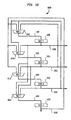
- FIG. 2 shows a block diagram of tag monitor system 222 located within a portion of superscalar unit 104 (shown as the inner dashed line in FIG. 2 ).
- Tag monitor system 222 includes: a register file 202 , a tag FIFO 204 and control logic 207 .
- Tag FIFO 204 is a multiple advance, multiple output, recycling FIFO that stores tags in a plurality of slots 206 .
- the term “multiple advance” means that the FIFO can be advanced any number of slots at a time. For example, a multiple advance 4-slot FIFO can be advanced 0-3 slots at a time.
- the term “multiple output” means that the contents of each slot of the FIFO are available.
- a tag is a unique label that superscalar unit 104 assigns to each instruction as it enters the instruction window.
- Tag FIFO 204 has one slot 206 for each instruction in the window.
- Each slot 206 has an output 232 that indicates (i.e., outputs) the value of the tag in the corresponding slot 206 .
- Each slot 206 also has a validity bit that indicates whether the instruction assigned to the tag in the slot 206 is valid.
- tag FIFO 204 contains eight slots 206 .
- Each of these slots 206 contains a unique binary number (tag) ranging from 0 to 7.
- a tag is three bits (e.g., 000, 001, 010, etc.) which, with the validity bit, causes each slot to hold four bits.
- each output 232 is four bits wide.
- Each slot 206 of tag FIFO 204 is loaded with a unique tag when the chip is powered-on or reset.
- tags are “recycled” or are recirculated in tag FIFO 204 .
- tags advance through the tag FIFO 204 from top 212 to bottom 210 .
- FIFO 204 is called a recycling queue.
- Register file 202 is coupled to tag FIFO 204 and instruction source 102 .
- Register file 202 stores instruction information sent by instruction source 102 .
- the following are examples of the type of information that can be sent from instruction source 102 to register file 202 : decoded instruction information; instruction functional unit requirements; the type of operation to be performed by the instruction; information specifying a storage location where instruction results are to be stored; information specifying a storage location where instruction operands are stored; information specifying a target address of a control flow instruction; and information specifying immediate data to be used in an operation specified by the instruction.
- Register file 202 includes: a write data port 214 , a write address port 216 , a write enable port 218 , a read address port 220 , and a read data port 224 .
- Write data port 214 receives instruction information from instruction source 102 via bus 103 .
- Write address ports 216 specify what addressable location in register file 202 the instruction information that is received through write data ports 214 is to be stored.
- Write address ports 216 are coupled to control logic 207 via a bus 226 .
- Write enable ports 218 indicate when to write data from instruction source 102 into register file 202 .
- Write enable ports are coupled to control logic 207 via bus 228 .
- register file 202 has four write data ports 214 labeled A through D.
- Write data ports 214 have corresponding write address ports 216 labeled A through D, and corresponding write enable ports 218 also labeled A through D.
- Read address port 220 is coupled to tag FIFO 204 via bus 230 .
- Bus 230 carries outputs 232 of each slot 206 of tag FIFO 204 .
- Read address ports 220 select the instruction information that will be accessed through read data ports 224 .
- Each read address port 220 has a corresponding read data port 224 .
- the instruction window has eight entries (i.e., the depth of tag FIFO 204 ) and register file 202 has one read address port 220 and one read data port 224 for each instruction in the window.
- Read address ports 220 are labeled 0 through 7 and their corresponding read data ports 224 are also labeled 0 through 7 .
- register file 202 is connected to other elements (e.g. an issuer not shown) located within superscalar environment 101 .
- Control logic 207 is comprised of logic circuits. Control logic 207 monitors functional unit 106 via a bus 234 and bus 230 from tag FIFO 204 . Control logic 207 signals instruction source 102 via bus 238 to send new instruction information to register file 202 as instructions leave the window. Control logic 207 indicates how many new instructions that instruction source 102 should send. In a preferred embodiment (shown in FIG. 2 ), the maximum number of instructions that can be sent is four, which corresponds to the total number of write data ports 214 in register file 202 . Control logic 207 will also synchronize tag FIFO 204 via a bus 236 to advance as instructions leave the window.
- tag FIFO 204 advances by as many steps as the number of instructions that leave the window at one time.
- the control logic 207 also maintains the validity bits stored in tag FIFO 204 via bus 236 .
- the circuit implementation for control logic 207 would be apparent to a person skilled in the relevant art. For example, currently well known and commercially available logic synthesis and layout systems can be used to convert a behavioral description (e.g., Verilog, manufactured by Cadence Design Systems, San Jose, Calif.) to a silicon or chip design.
- bit width of the various buses disclosed herein may support parallel or serial address or data transfer, the selection of which is implementation specific, as would be apparent to a person skilled in the relevant art.
- the tag monitor system may contain more than one register file.
- the instruction information is distributed among many register files.
- one register file contains the destination register addresses of each instruction.
- One advantage to using multiple register files is that it allows the designer to use smaller register files which can be located near where their contents are used. This can make the physical design of the processor easier.
- the register files' read and write addresses are all connected together and come from the same source. The write data of the register files still comes from the instruction source. However, not all of the register files have to hold all of the information for each instruction. The outputs of each register file only go to where the data held in that register file is needed.
- FIG. 4 shows a tag monitor system 222 that contains two register files 202 a and 202 b .
- only a portion of each instruction's information is stored in each register file 202 a and 202 b . So the data sent on bus 103 from the instruction source 102 is divided. One portion 103 a is sent to register file 202 a and the other 103 b is sent to register file 202 b .
- Both register files 202 a and 202 b are connected to buses 226 and 228 that provide control signals from the control logic 207 and to bus 230 that provides the outputs from tag FIFO 204 .
- the outputs of register files 202 a and 202 b are provided on separate buses 240 a and 240 b to different locations throughout the superscalar unit 104 .
- the tag FIFO 204 will now be described with the reference to example embodiments.
- FIG. 5 shows a diagram of a FIFO 500 .
- FIFO 500 holds four pieces of data in its four slots 504 , 508 , 512 , and 516 .
- the four slots are connected via buses 506 , 510 and 514 .
- FIFO 500 has an input 502 and an output 518 through which data enters and leaves the FIFO 500 .
- FIFO 500 behaves like a queue with four positions. When FIFO 500 advances, any data in slot 516 leaves FIFO 500 through output 518 . Data in slot 512 moves to slot 516 via bus 514 . Data in slot 508 moves to slot 512 via bus 510 . Data in slot 504 moves to slot 508 via bus 506 , and data on the input 502 moves into slot 504 . Each of these data transfers happens whenever FIFO 500 advances.
- FIG. 6 shows a diagram of a FIFO 600 with multiple outputs.
- FIFO 600 is structured much like FIFO 500 in FIG. 5 .
- Data enters FIFO 600 through an input 602 , moves through four slots 604 , 610 , 616 and 622 and then out through an output 626 .
- the difference between FIFO 500 and FIFO 600 is that the data stored in each slot 604 , 610 , 616 and 622 is visible on (i.e., can be read four) corresponding buses 606 , 612 , 618 or 624 from the time that it enters a respective slot until FIFO 600 advances again.
- Outputs 606 , 612 , 618 or 624 allow the user to know what data is stored in FIFO 600 at any given time.
- data stored in slots 604 , 610 , 616 and 622 is continuously visible on each slot's output bus (i.e., on buses 608 , 614 , 620 and 626 ). In this situation, buses 606 , 612 , 618 or 624 are unnecessary.
- FIG. 7 An example of this embodiment is shown in FIG. 7 .
- Buses 706 , 710 and 714 are used to convey data between slots 1 and 4 ( 704 , 708 , 712 and 716 , respectively) and also indicate the contents of slots 1 , 2 and 3 , 704 , 708 and 712 respectively.
- Output bus 718 always permits the contents of slot 716 to be read.
- FIG. 8 shows a recycling FIFO 800 .
- Recycling FIFO 800 also functions much like FIFO 500 in FIG. 5 .
- Recycle FIFO 800 comprises four slots 804 , 808 , 812 and 816 .
- the main difference is that when FIFO 800 advances, data in slot 816 moves to slot 804 .
- FIFO 800 Since FIFO 800 has no means for inputting new data into slot 804 , it must be designed so that when turned on or reset, each slot 804 , 808 , 812 and 816 is initialized with some value. These initial values then circulate through FIFO 800 until reinitialized in a known manner.
- FIFO sometimes it is necessary to advance a FIFO by more than one step at a time. Since the FIFO inputs one piece of data each time the FIFO advances on step, the FIFO must also have as many inputs as the maximum number of steps that the FIFO can advance. The FIFO must have some means besides buses to carry the data from each slot or input to the correct destination.
- FIG. 9 shows a multiple advance FIFO 900 .
- FIFO 900 is capable of advancing 1 , 2 , 3 , or 4 steps (i.e., slots) at one time.
- FIFO 900 has four inputs 902 , 904 , 906 and 908 , and four slots 914 , 922 , 930 and 938 .
- the data on input 902 goes to slot 938
- input 904 goes to slot 930
- input 906 goes to slot 922
- input 908 goes to slot 914 .
- FIFO 900 has four multiplexers: MUX 1 , MUX 2 , MUX 3 and MUX 4 , shown at 910 , 918 , 926 and 934 , respectively. These multiplexers are used to select the data that goes into each slot when FIFO 900 advances. Inputs to each multiplexer are the data that might need to go to its corresponding slot. For example, depending on the number of steps that FIFO 900 advances, the data from slot 914 , slot 922 , slot 930 or input 902 might go to slot 938 .
- the inputs to 934 are the outputs from slot 916 , slot 924 , slot 932 and input 902 .
- the structure and operation of the logic circuits necessary to control the multiplexers 910 , 918 , 926 and 934 would be apparent to a person skilled in the relevant art.
- FIG. 10 A diagram of recycling, multiple advance FIFO 1000 is shown in FIG. 10 .
- FIFO 1000 is capable of being advanced one, two or three steps at a time. Since FIFO 1000 has four stages (slots 1 - 4 , labeled 1006 , 1014 , 1022 and 1030 , respectively), advancing by four steps is logically the same as not advancing at all. Thus, since it never has to advance by four steps, the structure of the multiplexers in the recycling, multiple advance FIFO 1000 is different from that shown in the multiple advance FIFO 900 .
- FIFO 1000 is also a multiple output FIFO like FIFO 700 shown in FIG. 7 . Furthermore, like the recycling FIFO 800 in FIG. 8 , FIFO 1000 must also have some means for initialization.
- FIGS. 5 , 6 , 7 , 8 , 9 and 10 are all shown with four stages as an example. It is, of course, possible to modify these designs so that they contain a number of slots other than four. These modifications would be apparent to a person skilled in the relevant art.
- FIG. 3 is a flowchart illustrating the operation of tag monitor system 222 . Operational steps 310 - 312 will be described with reference to hardware elements of FIGS. 1 and 2 .
- control logic 207 sends a request data signal 238 requesting instruction source 102 to send instruction information.
- Control logic 207 requests information for a number of instructions equal to the number of empty spaces in the instruction window.
- control logic 207 determines how many new instructions can be added to the instruction window, and then requests sufficient instruction information from instruction source 102 to refill the empty top slots of the queue. There is a maximum number of instructions whose information can be sent that is less than the number of spaces in the window.
- actuate write enable and write address, assign tag and update validity bits In a step 304 , actuate write enable and write address, assign tag and update validity bits.
- Control logic 207 sends an enable signal on bus 226 and an address signal on bus 228 to write enable port 218 and write address port 216 , respectively.
- the addresses on each port 216 specify where the instruction information on the corresponding data port 214 should be stored in register file 202 during a step 306 .
- Instruction information is sent from instruction source 102 to register file 202 via bus 103 .
- the total number of enable bits on bus 226 equals the maximum number of instructions whose information can be sent at one time, which in the preferred embodiment is four.
- control logic 207 uses enable signals on bus 228 to select only the data that needs to be written. For example, if there is only one empty space at the top of the instruction window, then control logic 207 will send the tag contained in top slot 212 of the queue on bus 228 to write address port 216 A and assert write enable port 218 A via bus 226 . This operation causes only the instruction information on write data port 214 A to be stored in register file 202 in a location specified by the tag in top slot 212 of tag FIFO 204 .
- control logic 207 will send two enables to ports 218 A and 218 B and the two tags at the top of the window will be sent to write address ports 216 A and 216 B (the tag in top slot 212 going to 216 B), thus causing the instruction information on ports 214 A and 214 B to be stored in register file 202 .
- the instruction is said to have been “assigned” that tag.
- Control logic 207 also updates the validity bits in tag FIFO 204 during step 304 .
- control logic 207 will only assert the validity bits of the tags that were assigned to valid instructions in step 304 . For those tags that do not get assigned, their validity bits will remain unasserted until they are assigned to a valid instruction.
- a step 308 all of the contents of register file 202 are read through read data ports 224 . It is contemplated to use less than all the contents of register file 202 .
- the data that is to be read from register file 202 is specified by the addresses presented to register file 202 through read address ports 220 .
- the data is then used in the execution of some or all of the instructions in the window.
- read address 220 is always asserted. In other words, there is always a tag in each slot 206 .
- control logic 207 determines if any of the instructions executed in step 308 are ready to retire. If no instruction retires, data will continue to be read out of register file 202 and the instructions in the window will continue to be executed, as indicated by the “NO” path 311 of decisional step 310 . If an instruction does retire, control logic 207 will receive information indicating the number of instructions that are retiring via bus 234 as shown in a step 312 . The information received on bus 234 comes from a retirement unit (not shown). The details of the retirement unit are not relevant to carry out the present invention. (An example, however, of an instruction retirement unit is disclosed in U.S. Pat. No. 5,826,055). Control logic 207 then indicates, via bus 236 , how many steps tag FIFO 204 should advance.
- tag FIFO 204 will advance by one step.
- Tag I will move from bottom 210 to top 212 into Tag O's current location, and all other tags will be advanced accordingly.
- Tag 1 When Tag 1 is moved from the bottom 210 to the top 212 , its validity bit is deasserted.
- Tag 1 will be reassigned to the next new instruction to enter the instruction window.
- Tag 2 should be located at bottom 210 of tag FIFO 204 after step 312 . The operation of tag monitor system 222 will continue by returning to operational step 302 discussed above via branch 314 .
Landscapes
- Engineering & Computer Science (AREA)
- Software Systems (AREA)
- Theoretical Computer Science (AREA)
- Physics & Mathematics (AREA)
- General Engineering & Computer Science (AREA)
- General Physics & Mathematics (AREA)
- Advance Control (AREA)
- Executing Machine-Instructions (AREA)
Abstract
A tag monitoring system for assigning tags to instructions embodied in software on a tangible computer-readable storage medium. A source supplies instructions to be executed by a functional unit. A queue having a plurality of slots containing tags which are used for tagging instructions. A register file stores information required for the execution of each instruction at a location in the register file defined by the tag assigned to that instruction. A control unit monitors the completion of executed instructions and advances the tags in the queue upon completion of an executed instruction. The register file also contains a plurality of read address enable ports and corresponding read output ports. Each of the slots from the queue is coupled to a corresponding one of the read address enable ports. Thus, the information for each instruction can be read out of the register file in program order.
Description
This application is a continuation of U.S. patent application Ser. No. 11/338,817, filed Jan. 25, 2006, now U.S. Pat. No. 7,430,651, which is a continuation of U.S. patent application Ser. No. 10/847,460, filed May 18, 2004, now U.S. Pat. No. 7,043,624, which is a continuation of U.S. patent application Ser. No. 10/034,252, filed Jan. 3, 2002, now U.S. Pat. No. 6,757,808, which is a continuation of U.S. patent application Ser. No. 09/574,251, filed May 19, 2000, now U.S. Pat. No. 6,360,309, which is a continuation of U.S. patent application Ser. No. 09/252,655, filed Feb. 19, 1999, now U.S. Pat. No. 6,092,176, which is a continuation of U.S. patent application Ser. No. 08/811,237, filed Mar. 3, 1997, now U.S. Pat. No. 5,896,542, which is a continuation of U.S. patent application Ser. No. 08/224,328, filed Apr. 4, 1994, now U.S. Pat. No. 5,628,021, which is a continuation-in-part of U.S. patent application Ser. No. 07/999,648 filed Dec. 31, 1992, now U.S. Pat. No. 5,604,912. The entirety of each of the foregoing applications is incorporated by reference herein.
This application is related to U.S. patent application Ser. No. 08/799,462, filed Feb. 13, 1997, now U.S. Pat. No. 5,892,963, the entirety of which is incorporated by reference herein.
1. Field of the Invention
The present invention relates generally to superscalar computers, and more particularly, a system and method for using tags to control instruction execution in a superscalar reduced instruction set computer (RISC).
2. Related Art
Processors used in conventional computer systems typically execute program instructions one at a time, in sequential order. The process of executing a single instruction involves several sequential steps. The first step generally involves fetching the instruction from a memory device. The second step generally involves decoding the instruction, and assembling any operands.
The third step generally involves executing the instruction, and storing the results. Some processors are designed to perform each step in a single cycle of the processor clock. Alternatively, the processor may be designed so that the number of processor clock cycles per step depends on the particular instruction.
To improve performance, modern computers commonly use a technique known as pipelining. Pipelining involves the overlapping of the sequential steps of the execution process. For example, while the processor is performing the execution step for one instruction, it might simultaneously perform the decode step for a second instruction, and perform a fetch of a third instruction. Pipelining can thus decrease the execution time for a sequence of instructions.
Another class of processors improve performance by overlapping the sub-steps of the three sequential steps discussed above are called superpipelined processors.
Still another technique for improving performance involves executing multiple instructions simultaneously. Processors which utilize this technique are generally referred to as superscalar processors. The ability of a superscalar processor to execute two or more instructions simultaneously depends on the particular instructions being executed. For example, two instructions which both require use of the same, limited processor resource (such as the floating point unit) cannot be executed simultaneously. This type of conflict is known as a resource dependency. Additionally, an instruction which uses the result produced by the execution of another instruction cannot be executed at the same time as the other instruction. An instruction which depends on the result of another instruction is said to have a data dependency on the other instruction. Similarly, an instruction set may specify that particular types of instructions must execute in a certain order relative to each other. These instructions are said to have procedural dependencies.
A third technique for improving performance involves executing instructions out of program order. Processors which utilize this technique are generally referred to as out-of-order processors. Usually, out-of-order processors are also superscalar processors. Data dependencies and procedural dependencies limit out-of-order execution in the same way that they limit superscalar execution.
From here on, the term “superscalar processor” will be used to refer to a processor that is: capable of executing multiple instructions simultaneously, or capable of executing instructions out of program order, or capable of doing both.
For executing instructions either simultaneously or out of order, a superscalar processor must contain a system called an Execution unit. The Execution Unit contains multiple functional units for executing instructions (e.g., floating point multiplier, adder, etc.). Scheduling control is needed to dispatch instructions to the multiple functional units. With in-order issue, the processor stops decoding instructions whenever a decoded instruction creates a resource conflict or has a true dependency or an output dependency on a uncompleted instruction. As a result, the processor is not able to look ahead beyond the instructions with the conflict or dependency, even though one or more subsequent instructions might be executable. To overcome this limitation, processors isolate the decoder from the execution stage, so that it continues to decode instructions regardless of whether they can be executed immediately. This isolation is accomplished by a buffer between the decode and execute stages, called an instruction window.
To take advantage of lookahead, the processor decodes instructions and places them into the window as long as there is room in the window and, at the same time, examines instructions in the window to find instructions that can be executed (that is, instructions that do not have resource conflicts or dependencies). The instruction window serves as a pool of instructions, giving the processor lookahead ability that is constrained only by the size of the window and the capability of the instruction source. Thus, out-of-order issue requires a buffer, called an instruction window between the decoder and functional units; and the instruction window provides a snap-shot of a piece of the program that the computer is executing.
After the instructions have finished executing, instructions must be removed from the window so that new instructions can take their place. Current designs employ an instruction window that utilizes a First In First Out queue (FIFO). In certain designs, the new instructions enter the window and completed instructions leave the window in fixed size groups. For example, an instruction window might contain eight instructions (I0-I7) and instructions may be changed in groups of four. In this case, after instructions I0, I1, I2 and I3 have executed, they are removed from the window at the same time four new instructions are advanced into the window. Instruction windows where instructions enter and leave in fixed size groups are called “Fixed Advance Instruction Windows.”
In other types of designs, the new instructions enter the window and completed instructions leave the window in groups of various sizes. For example, an instruction window might contain eight instructions (I0-I7) and may be changed in groups of one, two or three. In this case, after any of instructions I0, I1 or I2 have executed, they can be removed from the window and new instructions can be advanced into the window. Instruction windows where instructions enter and leave in groups of various sizes are called “Variable Advance Instruction Windows.”
Processors that use Variable Advance Instruction Windows (VAIW) tend to have higher performance than processors that have Fixed Advance Instruction Windows (FAIW). However, fixed advance instruction windows are easier for a processor to manage since a particular instruction can only occupy a fixed number of locations in the window. For example, in an instruction window that contains eight instructions (I0-I7) and where instructions can be added or removed in groups of four, an instruction can occupy only one of two locations in the window (e.g., I0 and I4). In a variable advance instruction windows, that instruction could occupy all of the locations in the window at different times, thus a processor that has a variable advance instruction window must have more resources to track each instruction's position than a processor that has a fixed advance instruction window.
Current designs use large queues to implement the instruction window. The idea of using queues is disadvantageous, for many reasons including: a large amount of chip area resources are dedicated to a plurality of queues especially when implementing a variable advance instruction window; there is limited flexibility in designing a system with more than one queue; and control logic for directing data in queues is complex and inflexible.
Therefore, what is needed is a technique to “track” or monitor instructions as they move through the window. The system must be flexible and require a small area on a chip.
The present invention is directed to a technique for monitoring instruction execution of multiple instructions in parallel and out of program order using a system that assigns tags to the multiple instructions and maintains an instruction window that contains the multiple instructions. The system is a component of a superscalar unit which is coupled between a source of instructions and functional units which execute the instructions. The superscalar unit is in charge of maintaining the instruction window, directing instructions to the various functional units in the execution unit, and, after the instructions are executed, receiving new instructions from the source.
The present invention employs a tag monitor system, which is a part of the superscalar unit. The tag monitor system includes: a register file and a queue that operates on a First-In-First-Out basis (the queue is a multiple-advance, multiple output, recycling FIFO). The queue is coupled to the register file. The register file is coupled to the instruction source and is used to store instruction information (i.e., the resource requirements of each instruction). When an instruction is sent from the instruction source to the register file it is assigned a tag that is not currently assigned to any other instruction. The instruction information is then stored in the register file at an address location indicated by the tag of the instruction. Once an instruction's information is stored in the register file, it is said to be “in the instruction window.” The tags of each instruction in the instruction window are stored in the queue. The tags are arranged in the queue in the same order as their corresponding instructions are arranged in the program.
When an instruction is finished, the queue advances and the tag of the instruction is effectively pushed out the bottom of the queue. The tag can then be reassigned to a new instruction that enters the instruction window. Accordingly, the tag is sent back to the top of the queue (in other words, it is recycled). It is also possible for several tags to be recycled at the same time when several instructions finish at the same time. In a preferred embodiment, instructions are required to finish in order. This is often necessary to prevent an instruction from incorrectly overwriting the result of another instruction. For example, if a program contains two instructions that write to the same location of memory, then the instruction that comes first in the program should write to the memory before the second. Thus, the results of instructions that are executed out of order must be held in some temporary storage area and the instructions themselves must remain in the instruction window until all previous instruction have been executed. When a group of instructions is completed, all of their results are moved from the temporary storage area to their real destinations. Then the instructions are removed from the window and their tags are recycled.
The register file has write ports where new instruction information is received from the instruction source. The register file has a number of write ports equal to the number of new instructions that can be added to the window at one time. The register file has one entry for each instruction in the window. The register file also has one output port for every instruction in the window. Associated with each output port is an address port. The address port is used to select which register file entry's contents will be output on its corresponding output port.
The queue has an output for each slot (e.g., specific buffer location in the queue) that shows the value of the tag stored in that slot. These outputs are connected to the read address ports of the register file. This connection causes the register file to provide an entry's contents on its corresponding output port when a tag value is presented by the queue to the read address ports. The outputs of the register file are sent to various locations in the superscalar unit and execution units where the instruction information is used for instruction scheduling, instruction execution, and the like.
It is possible that some of the locations in the instruction window may be empty at any given time. These empty window locations are called “bubbles.” Bubbles sometimes occur when an instruction leaves the window and the instruction source cannot immediately send another instruction to replace it. If there are bubbles in the window, then some of the entries in the register file will contain old or bogus instruction information. Since all of the data in the register file is always available, there needs to be some way to qualify the data in the register file.
According to the present invention, a “validity bit” is associated with each entry in the instruction window to indicate if the corresponding instruction information in the register file is valid. These validity bits can be held in the tag FIFO with the tags. There is one validity bit for each tag in the FIFO. These bits are updated each time a tag is recycled. If, when a tag is recycled, it gets assigned to a valid instruction, then the bit is asserted. Otherwise it is deasserted.
The validity bits are output from the tag monitor system along with the outputs of the register file. They are sent to the same locations as the outputs of the register file so that the superscalar unit or execution units will know if they can use the instruction information.
A feature of the present invention is that an instruction window can be maintained without storing instruction information in large queues. This simplifies design and increases operational flexibility. For example, for a window containing n instructions, the tag monitor system would contain a queue with n entries and a register file with n entries and n output ports. If each output of the queue is connected to its corresponding read address port on the register file (e.g., output 0 connected to read address port 0, output 1 connected to read address port 1, etc.) then the register file outputs will “display” (i.e., make available at the output ports) the information for each instruction in the window in program order (e.g., output port 0 will show instruction 0's information, output port 1 will show instruction 1's information, etc.). When the window advances, the queue advances and the addresses on the read address ports change. This causes the outputs of the register file to change to reflect the new arrangement of instructions in the window. It is necessary for the instruction information to be displayed in order on the register file outputs so that it can be sent to the rest of the superscalar unit in order. The superscalar unit needs to know the order of the instructions in the window so that it can schedule their execution and their completion.
Further features and advantages of the present invention, as well as the structure and operation of various embodiments of the present invention, are described in detail below with reference to the accompanying drawings.
1.0 System Environment
The buses shown in FIG. 1 represent data and control signals. Bus and instruction size may vary depending on the application. The remaining discussion will be focused on a tag monitor system, which tracks instructions for superscalar unit 104.
2.0 Structure and Operation of the Tag Monitor System
A. Structure
Once a tag is assigned to an instruction, it will remain with that instruction until the instruction is removed from the window. Once an instruction is removed from the window, its tag is sent back to the top 212 of tag FIFO 204. The tag sent to top 212 can be reassigned to a new instruction that enters the window. In this fashion, tags are “recycled” or are recirculated in tag FIFO 204. Generally, tags advance through the tag FIFO 204 from top 212 to bottom 210. Thus, FIFO 204 is called a recycling queue.
Write data port 214 receives instruction information from instruction source 102 via bus 103. Write address ports 216 specify what addressable location in register file 202 the instruction information that is received through write data ports 214 is to be stored. Write address ports 216 are coupled to control logic 207 via a bus 226. Write enable ports 218 indicate when to write data from instruction source 102 into register file 202. Write enable ports are coupled to control logic 207 via bus 228. In a preferred embodiment (shown in FIG. 2 ) register file 202 has four write data ports 214 labeled A through D. Write data ports 214 have corresponding write address ports 216 labeled A through D, and corresponding write enable ports 218 also labeled A through D.
Read address port 220 is coupled to tag FIFO 204 via bus 230. Bus 230 carries outputs 232 of each slot 206 of tag FIFO 204. Read address ports 220 select the instruction information that will be accessed through read data ports 224. Each read address port 220 has a corresponding read data port 224. In a preferred embodiment (shown in FIG. 2 ), the instruction window has eight entries (i.e., the depth of tag FIFO 204) and register file 202 has one read address port 220 and one read data port 224 for each instruction in the window. Read address ports 220 are labeled 0 through 7 and their corresponding read data ports 224 are also labeled 0 through 7.
Typically, register file 202 is connected to other elements (e.g. an issuer not shown) located within superscalar environment 101.
Note that the bit width of the various buses disclosed herein may support parallel or serial address or data transfer, the selection of which is implementation specific, as would be apparent to a person skilled in the relevant art.
It is also possible for the tag monitor system to contain more than one register file. In a preferred embodiment, the instruction information is distributed among many register files. For example, one register file contains the destination register addresses of each instruction. Another contains the functional unit requirements of each instruction and so on. One advantage to using multiple register files is that it allows the designer to use smaller register files which can be located near where their contents are used. This can make the physical design of the processor easier. The register files' read and write addresses are all connected together and come from the same source. The write data of the register files still comes from the instruction source. However, not all of the register files have to hold all of the information for each instruction. The outputs of each register file only go to where the data held in that register file is needed.
The tag FIFO 204 will now be described with the reference to example embodiments.
In a preferred embodiment, data stored in slots 604, 610, 616 and 622 is continuously visible on each slot's output bus (i.e., on buses 608, 614, 620 and 626). In this situation, buses 606, 612, 618 or 624 are unnecessary. An example of this embodiment is shown in FIG. 7 . Buses 706, 710 and 714 are used to convey data between slots 1 and 4 (704, 708, 712 and 716, respectively) and also indicate the contents of slots 1, 2 and 3, 704, 708 and 712 respectively. Output bus 718 always permits the contents of slot 716 to be read.
Sometimes it is necessary to advance a FIFO by more than one step at a time. Since the FIFO inputs one piece of data each time the FIFO advances on step, the FIFO must also have as many inputs as the maximum number of steps that the FIFO can advance. The FIFO must have some means besides buses to carry the data from each slot or input to the correct destination.
In order to advance more than one step at a time, the inputs must be switchably connected to each slot and the outputs of some slots must go to more than one other slot. Therefore, FIFO 900 has four multiplexers: MUX1, MUX2, MUX3 and MUX4, shown at 910, 918, 926 and 934, respectively. These multiplexers are used to select the data that goes into each slot when FIFO 900 advances. Inputs to each multiplexer are the data that might need to go to its corresponding slot. For example, depending on the number of steps that FIFO 900 advances, the data from slot 914, slot 922, slot 930 or input 902 might go to slot 938. Thus the inputs to 934 are the outputs from slot 916, slot 924, slot 932 and input 902. The structure and operation of the logic circuits necessary to control the multiplexers 910, 918, 926 and 934 would be apparent to a person skilled in the relevant art.
It is also possible to design a multiple advance FIFO that recycles its contents. This FIFO is a combination of the FIFOs shown in FIGS. 8 and 9 . A diagram of recycling, multiple advance FIFO 1000 is shown in FIG. 10 . FIFO 1000 is capable of being advanced one, two or three steps at a time. Since FIFO 1000 has four stages (slots 1-4, labeled 1006, 1014, 1022 and 1030, respectively), advancing by four steps is logically the same as not advancing at all. Thus, since it never has to advance by four steps, the structure of the multiplexers in the recycling, multiple advance FIFO 1000 is different from that shown in the multiple advance FIFO 900. FIFO 1000 is also a multiple output FIFO like FIFO 700 shown in FIG. 7 . Furthermore, like the recycling FIFO 800 in FIG. 8 , FIFO 1000 must also have some means for initialization.
The FIFOs shown in FIGS. 5 , 6, 7, 8, 9 and 10 are all shown with four stages as an example. It is, of course, possible to modify these designs so that they contain a number of slots other than four. These modifications would be apparent to a person skilled in the relevant art.
B. Operation
Operation starts at a step 301. In a step 302, control logic 207 sends a request data signal 238 requesting instruction source 102 to send instruction information. Control logic 207 requests information for a number of instructions equal to the number of empty spaces in the instruction window. In a preferred embodiment, in effect, control logic 207 determines how many new instructions can be added to the instruction window, and then requests sufficient instruction information from instruction source 102 to refill the empty top slots of the queue. There is a maximum number of instructions whose information can be sent that is less than the number of spaces in the window.
In a step 304, actuate write enable and write address, assign tag and update validity bits. Control logic 207 sends an enable signal on bus 226 and an address signal on bus 228 to write enable port 218 and write address port 216, respectively. The addresses on each port 216 specify where the instruction information on the corresponding data port 214 should be stored in register file 202 during a step 306. Instruction information is sent from instruction source 102 to register file 202 via bus 103. Typically, the total number of enable bits on bus 226 equals the maximum number of instructions whose information can be sent at one time, which in the preferred embodiment is four.
The address where each instruction's information is stored in register file 202 is specified by the tag of that instruction. Since the data on write data ports 214 does not always need to be stored in register file 202, control logic 207 uses enable signals on bus 228 to select only the data that needs to be written. For example, if there is only one empty space at the top of the instruction window, then control logic 207 will send the tag contained in top slot 212 of the queue on bus 228 to write address port 216A and assert write enable port 218A via bus 226. This operation causes only the instruction information on write data port 214A to be stored in register file 202 in a location specified by the tag in top slot 212 of tag FIFO 204. If there are two empty spaces in the instruction window, then control logic 207 will send two enables to ports 218A and 218B and the two tags at the top of the window will be sent to write address ports 216A and 216B (the tag in top slot 212 going to 216B), thus causing the instruction information on ports 214A and 214B to be stored in register file 202. When an instruction's information is stored in a location in register file 202 specified by a tag, the instruction is said to have been “assigned” that tag. Control logic 207 also updates the validity bits in tag FIFO 204 during step 304. If instruction source 102 cannot supply an instruction for every request made in step 302, control logic 207 will only assert the validity bits of the tags that were assigned to valid instructions in step 304. For those tags that do not get assigned, their validity bits will remain unasserted until they are assigned to a valid instruction.
In a step 308, all of the contents of register file 202 are read through read data ports 224. It is contemplated to use less than all the contents of register file 202. The data that is to be read from register file 202 is specified by the addresses presented to register file 202 through read address ports 220. The data is then used in the execution of some or all of the instructions in the window. In a preferred embodiment, read address 220 is always asserted. In other words, there is always a tag in each slot 206.
In a decisional step 310, control logic 207 determines if any of the instructions executed in step 308 are ready to retire. If no instruction retires, data will continue to be read out of register file 202 and the instructions in the window will continue to be executed, as indicated by the “NO” path 311 of decisional step 310. If an instruction does retire, control logic 207 will receive information indicating the number of instructions that are retiring via bus 234 as shown in a step 312. The information received on bus 234 comes from a retirement unit (not shown). The details of the retirement unit are not relevant to carry out the present invention. (An example, however, of an instruction retirement unit is disclosed in U.S. Pat. No. 5,826,055). Control logic 207 then indicates, via bus 236, how many steps tag FIFO 204 should advance.
Referring to FIG. 2 , if one instruction retires, then tag FIFO 204 will advance by one step. Tag I will move from bottom 210 to top 212 into Tag O's current location, and all other tags will be advanced accordingly. When Tag 1 is moved from the bottom 210 to the top 212, its validity bit is deasserted. Tag 1 will be reassigned to the next new instruction to enter the instruction window. Tag 2 should be located at bottom 210 of tag FIFO 204 after step 312. The operation of tag monitor system 222 will continue by returning to operational step 302 discussed above via branch 314.
While various embodiments of the present invention have been described above, it should be understood that they have been presented by way of example, and not limitation. Thus the breadth and scope of the present invention should not be limited by any of the above-described exemplary embodiments, but should be defined only in accordance with the following claims and their equivalents.
Claims (18)
1. A non-transitory computer-readable storage medium having instructions stored thereon, the instructions being configured when executed to design a system configured to track instructions in a variable advance instruction window, the instructions comprising:
a storage medium instruction embodied in a behavioral description, the instruction converting the behavioral description to a chip design with an instruction source of the system, the instruction source being configured to provide a plurality of items of instruction information, wherein each of the plurality of items of instruction information pertain to an instruction to be executed;
a storage medium instruction embodied in a behavioral description, the instruction converting the behavioral description to a chip design with a plurality of register files of the system, the plurality of register files being coupled to the instruction source; and
a storage medium instruction embodied in a behavioral description, the instruction converting the behavioral description to a chip design with control logic of the system, the control logic being configured to couple the instruction source and the plurality of register files, the control logic adapted to selectively route each of the plurality of information items for storage in one or more of the plurality of register files, wherein each of the plurality of register files stores at least one of the plurality of items of instruction information and wherein each of the plurality of items of instruction information is stored in a location in a register file that is uniquely addressable by a unique identifier assigned to the instruction to be executed.
2. The non-transitory computer-readable storage medium of claim 1 , wherein the instruction source comprises an instruction decoder.
3. The non-transitory computer-readable storage medium of claim 1 , wherein the plurality of items of instruction information includes decoded information pertaining to the instruction to be executed.
4. The non-transitory computer-readable storage medium of claim 1 , wherein the plurality of items of instruction information includes functional unit requirements for the instruction to be executed.
5. The non-transitory computer-readable storage medium of claim 1 , wherein the plurality of items of instruction information includes a type of operation to be performed by the instruction to be executed.
6. The non-transitory computer-readable storage medium of claim 1 , wherein the plurality of items of instruction information includes information specifying a storage location at which a result of the instruction to be executed is to be stored.
7. The non-transitory computer-readable storage medium of claim 1 , wherein the plurality of items of instruction information includes information specifying a storage location at which an operand of the instruction to be executed is stored.
8. The non-transitory computer-readable storage medium of claim 1 , wherein the plurality of items of instruction information includes information specifying a target address of the instruction to be executed.
9. The non-transitory computer-readable storage medium of claim 1 , wherein the plurality of items of instruction information includes information specifying immediate data to be used in an operation specified by the instruction to be executed.
10. The non-transitory computer-readable storage medium of claim 1 , wherein the control logic is further adapted to store the unique identifier assigned to the instruction to be executed in a slot in a recycling queue, wherein the recycling queue comprises a plurality of slots equal in number to a predetermined number of storage locations in each of the plurality of register files.
11. A non-transitory computer-readable storage medium that includes instructions configured when executed to generate a model of a system configured to control instruction processing in a superscaler processor, the instructions comprising:
a storage medium instruction embodied in a behavioral description, the instruction converting the behavioral description to a chip design with an instruction source in the system, the instruction source configured to supply instructions to be executed by the superscaler processor;
a storage medium instruction embodied in a behavioral description, the instruction converting the behavioral description to a chip design with a register file in the system, the register file comprising a plurality of buffer locations and a plurality of output ports; and
a storage medium instruction embodied in a behavioral description, the instruction converting the behavioral description to a chip design with a queue in the system, the queue comprising a plurality of slots, each of said plurality of slots storing a tag, wherein each tag stored in said queue identifies a unique one of said plurality of buffer locations,
wherein each instruction supplied by said instruction store is associated with one of said tags until said instruction retires, and
wherein at least a part of said instruction is stored in the buffer location identified by the tag to which said instruction is associated.
12. The non-transitory computer-readable storage medium of claim 11 , wherein each of said plurality of output ports is associated with a unique one of said slots of said queue, such that the output of any one of said output ports is the item stored in the buffer location identified by the tag that is stored in the slot associated with said any one of said output ports.
13. The non-transitory computer-readable storage medium of claim 11 , wherein said queue comprises four slots.
14. The non-transitory computer-readable storage medium of claim 13 , wherein said register file comprises four output ports.
15. The non-transitory computer-readable medium of claim 11 , wherein the number of output ports of said register file is equal to the number of slots of said queue.
16. The non-transitory computer-readable storage medium of claim 11 , wherein said queue is a recycling queue.
17. The non-transitory computer-readable storage medium of claim 16 , wherein if an instruction retires each of said tags in said queue, except a tag in a top slot of said queue, moves up one slot, and said tag in said top slot of said queue moves to a bottom slot of said queue.
18. The non-transitory computer-readable storage medium of claim 16 , wherein if an instruction retires each of said tags in said queue, except a tag in a bottom slot of said queue, moves down one slot, and said tag in said bottom slot of said queue moves to a top slot of said queue.
Priority Applications (1)
| Application Number | Priority Date | Filing Date | Title |
|---|---|---|---|
| US12/210,738 US8074052B2 (en) | 1992-12-31 | 2008-09-15 | System and method for assigning tags to control instruction processing in a superscalar processor |
Applications Claiming Priority (9)
| Application Number | Priority Date | Filing Date | Title |
|---|---|---|---|
| US07/999,648 US5604912A (en) | 1992-12-31 | 1992-12-31 | System and method for assigning tags to instructions to control instruction execution |
| US08/224,328 US5628021A (en) | 1992-12-31 | 1994-04-04 | System and method for assigning tags to control instruction processing in a superscalar processor |
| US08/811,237 US5896542A (en) | 1992-12-31 | 1997-03-03 | System and method for assigning tags to control instruction processing in a superscalar processor |
| US09/252,655 US6092176A (en) | 1992-12-31 | 1999-02-19 | System and method for assigning tags to control instruction processing in a superscalar processor |
| US09/574,251 US6360309B1 (en) | 1992-12-31 | 2000-05-19 | System and method for assigning tags to control instruction processing in a superscalar processor |
| US10/034,252 US6757808B2 (en) | 1992-12-31 | 2002-01-03 | System and method for assigning tags to control instruction processing in a superscalar processor |
| US10/847,460 US7043624B2 (en) | 1992-12-31 | 2004-05-18 | System and method for assigning tags to control instruction processing in a superscalar processor |
| US11/338,817 US7430651B2 (en) | 1992-12-31 | 2006-01-25 | System and method for assigning tags to control instruction processing in a superscalar processor |
| US12/210,738 US8074052B2 (en) | 1992-12-31 | 2008-09-15 | System and method for assigning tags to control instruction processing in a superscalar processor |
Related Parent Applications (1)
| Application Number | Title | Priority Date | Filing Date |
|---|---|---|---|
| US11/338,817 Continuation US7430651B2 (en) | 1992-12-31 | 2006-01-25 | System and method for assigning tags to control instruction processing in a superscalar processor |
Publications (2)
| Publication Number | Publication Date |
|---|---|
| US20090013158A1 US20090013158A1 (en) | 2009-01-08 |
| US8074052B2 true US8074052B2 (en) | 2011-12-06 |
Family
ID=22840187
Family Applications (8)
| Application Number | Title | Priority Date | Filing Date |
|---|---|---|---|
| US08/224,328 Expired - Lifetime US5628021A (en) | 1992-12-31 | 1994-04-04 | System and method for assigning tags to control instruction processing in a superscalar processor |
| US08/811,237 Expired - Lifetime US5896542A (en) | 1992-12-31 | 1997-03-03 | System and method for assigning tags to control instruction processing in a superscalar processor |
| US09/252,655 Expired - Lifetime US6092176A (en) | 1992-12-31 | 1999-02-19 | System and method for assigning tags to control instruction processing in a superscalar processor |
| US09/574,251 Expired - Fee Related US6360309B1 (en) | 1992-12-31 | 2000-05-19 | System and method for assigning tags to control instruction processing in a superscalar processor |
| US10/034,252 Expired - Fee Related US6757808B2 (en) | 1992-12-31 | 2002-01-03 | System and method for assigning tags to control instruction processing in a superscalar processor |
| US10/847,460 Expired - Fee Related US7043624B2 (en) | 1992-12-31 | 2004-05-18 | System and method for assigning tags to control instruction processing in a superscalar processor |
| US11/338,817 Expired - Fee Related US7430651B2 (en) | 1992-12-31 | 2006-01-25 | System and method for assigning tags to control instruction processing in a superscalar processor |
| US12/210,738 Expired - Fee Related US8074052B2 (en) | 1992-12-31 | 2008-09-15 | System and method for assigning tags to control instruction processing in a superscalar processor |
Family Applications Before (7)
| Application Number | Title | Priority Date | Filing Date |
|---|---|---|---|
| US08/224,328 Expired - Lifetime US5628021A (en) | 1992-12-31 | 1994-04-04 | System and method for assigning tags to control instruction processing in a superscalar processor |
| US08/811,237 Expired - Lifetime US5896542A (en) | 1992-12-31 | 1997-03-03 | System and method for assigning tags to control instruction processing in a superscalar processor |
| US09/252,655 Expired - Lifetime US6092176A (en) | 1992-12-31 | 1999-02-19 | System and method for assigning tags to control instruction processing in a superscalar processor |
| US09/574,251 Expired - Fee Related US6360309B1 (en) | 1992-12-31 | 2000-05-19 | System and method for assigning tags to control instruction processing in a superscalar processor |
| US10/034,252 Expired - Fee Related US6757808B2 (en) | 1992-12-31 | 2002-01-03 | System and method for assigning tags to control instruction processing in a superscalar processor |
| US10/847,460 Expired - Fee Related US7043624B2 (en) | 1992-12-31 | 2004-05-18 | System and method for assigning tags to control instruction processing in a superscalar processor |
| US11/338,817 Expired - Fee Related US7430651B2 (en) | 1992-12-31 | 2006-01-25 | System and method for assigning tags to control instruction processing in a superscalar processor |
Country Status (3)
| Country | Link |
|---|---|
| US (8) | US5628021A (en) |
| JP (8) | JP3561915B2 (en) |
| WO (1) | WO1995027247A1 (en) |
Cited By (9)
| Publication number | Priority date | Publication date | Assignee | Title |
|---|---|---|---|---|
| US20170177368A1 (en) * | 2015-12-17 | 2017-06-22 | Charles Stark Draper Laboratory, Inc. | Techniques for metadata processing |
| US10936713B2 (en) * | 2015-12-17 | 2021-03-02 | The Charles Stark Draper Laboratory, Inc. | Techniques for metadata processing |
| US11150910B2 (en) | 2018-02-02 | 2021-10-19 | The Charles Stark Draper Laboratory, Inc. | Systems and methods for policy execution processing |
| US11748457B2 (en) | 2018-02-02 | 2023-09-05 | Dover Microsystems, Inc. | Systems and methods for policy linking and/or loading for secure initialization |
| US11797398B2 (en) | 2018-04-30 | 2023-10-24 | Dover Microsystems, Inc. | Systems and methods for checking safety properties |
| US11841956B2 (en) | 2018-12-18 | 2023-12-12 | Dover Microsystems, Inc. | Systems and methods for data lifecycle protection |
| US11875180B2 (en) | 2018-11-06 | 2024-01-16 | Dover Microsystems, Inc. | Systems and methods for stalling host processor |
| US12040967B2 (en) | 2022-01-25 | 2024-07-16 | Bank Of America Corporation | System and method for splitting data elements for data communication based on transformation types implemented on the data elements at different devices |
| US12079197B2 (en) | 2019-10-18 | 2024-09-03 | Dover Microsystems, Inc. | Systems and methods for updating metadata |
Families Citing this family (52)
| Publication number | Priority date | Publication date | Assignee | Title |
|---|---|---|---|---|
| US5539911A (en) | 1991-07-08 | 1996-07-23 | Seiko Epson Corporation | High-performance, superscalar-based computer system with out-of-order instruction execution |
| US5493687A (en) | 1991-07-08 | 1996-02-20 | Seiko Epson Corporation | RISC microprocessor architecture implementing multiple typed register sets |
| EP0636256B1 (en) | 1992-03-31 | 1997-06-04 | Seiko Epson Corporation | Superscalar risc processor instruction scheduling |
| DE69308548T2 (en) | 1992-05-01 | 1997-06-12 | Seiko Epson Corp | DEVICE AND METHOD FOR COMPLETING THE COMMAND IN A SUPER-SCALAR PROCESSOR. |
| EP0682789B1 (en) | 1992-12-31 | 1998-09-09 | Seiko Epson Corporation | System and method for register renaming |
| US5604912A (en) * | 1992-12-31 | 1997-02-18 | Seiko Epson Corporation | System and method for assigning tags to instructions to control instruction execution |
| US5628021A (en) * | 1992-12-31 | 1997-05-06 | Seiko Epson Corporation | System and method for assigning tags to control instruction processing in a superscalar processor |
| JP3494484B2 (en) * | 1994-10-12 | 2004-02-09 | 株式会社ルネサステクノロジ | Instruction processing unit |
| US5675758A (en) | 1994-11-15 | 1997-10-07 | Advanced Micro Devices, Inc. | Processor having primary integer execution unit and supplemental integer execution unit for performing out-of-order add and move operations |
| US5712997A (en) * | 1996-01-31 | 1998-01-27 | Sun Microsystems, Inc | System and method for processing load instruction in accordance with "no-fault " processing facility including arrangement for preserving access fault indicia |
| US5859992A (en) * | 1997-03-12 | 1999-01-12 | Advanced Micro Devices, Inc. | Instruction alignment using a dispatch list and a latch list |
| US5878242A (en) * | 1997-04-21 | 1999-03-02 | International Business Machines Corporation | Method and system for forwarding instructions in a processor with increased forwarding probability |
| US5983341A (en) * | 1997-04-25 | 1999-11-09 | International Business Machines Corporation | Data processing system and method for extending the time for execution of an instruction |
| US5860018A (en) * | 1997-06-25 | 1999-01-12 | Sun Microsystems, Inc. | Method for tracking pipeline resources in a superscalar processor |
| US6035388A (en) | 1997-06-27 | 2000-03-07 | Sandcraft, Inc. | Method and apparatus for dual issue of program instructions to symmetric multifunctional execution units |
| US6112293A (en) * | 1997-11-17 | 2000-08-29 | Advanced Micro Devices, Inc. | Processor configured to generate lookahead results from operand collapse unit and for inhibiting receipt/execution of the first instruction based on the lookahead result |
| US6304959B1 (en) | 1999-03-05 | 2001-10-16 | International Business Machines Corporation | Simplified method to generate BTAGs in a decode unit of a processing system |
| US6425069B1 (en) * | 1999-03-05 | 2002-07-23 | International Business Machines Corporation | Optimization of instruction stream execution that includes a VLIW dispatch group |
| US6336182B1 (en) * | 1999-03-05 | 2002-01-01 | International Business Machines Corporation | System and method for utilizing a conditional split for aligning internal operation (IOPs) for dispatch |
| JP2001092657A (en) * | 1999-09-22 | 2001-04-06 | Toshiba Corp | Central arithmetic unit and compile method and recording medium recording compile program |
| US6691240B1 (en) * | 1999-12-30 | 2004-02-10 | Texas Instruments Incorporated | System and method of implementing variabe length delay instructions, which prevents overlapping lifetime information or values in efficient way |
| GB0002848D0 (en) * | 2000-02-08 | 2000-03-29 | Siroyan Limited | Communicating instruction results in processors and compiling methods for processors |
| US6785802B1 (en) | 2000-06-01 | 2004-08-31 | Stmicroelectronics, Inc. | Method and apparatus for priority tracking in an out-of-order instruction shelf of a high performance superscalar microprocessor |
| GB2367406B (en) | 2000-06-13 | 2002-06-05 | Siroyan Ltd | Predicated execution of instructions in processors |
| US6804815B1 (en) * | 2000-09-18 | 2004-10-12 | Cisco Technology, Inc. | Sequence control mechanism for enabling out of order context processing |
| US6813704B1 (en) * | 2001-12-20 | 2004-11-02 | Lsi Logic Corporation | Changing instruction order by reassigning only tags in order tag field in instruction queue |
| US20040181651A1 (en) * | 2003-03-11 | 2004-09-16 | Sugumar Rabin A. | Issue bandwidth in a multi-issue out-of-order processor |
| WO2004092720A1 (en) * | 2003-03-25 | 2004-10-28 | Arkray Inc. | Sensor-receiving container |
| JP2005038016A (en) | 2003-07-15 | 2005-02-10 | Canon Inc | Data processor, method and program, and image forming device |
| EP1548537A1 (en) * | 2003-12-23 | 2005-06-29 | STMicroelectronics Limited | Secure processor arrangement |
| SE0401922L (en) | 2004-07-23 | 2005-05-31 | Kvaser Consultant Ab | Device for time stamping of reference events |
| KR20080078255A (en) * | 2007-02-22 | 2008-08-27 | 삼성전자주식회사 | Method and apparatus of managing files and information storage medium storing files |
| EP2140047B1 (en) * | 2007-03-23 | 2011-01-12 | Solvay Advanced Polymers, L.L.C. | Improved fabrics |
| EP2129820B1 (en) * | 2007-03-23 | 2011-05-25 | Solvay Advanced Polymers, L.L.C. | Use of coal combustion flue gas filters |
| US7831784B2 (en) * | 2007-07-16 | 2010-11-09 | Apple Inc. | Managing purgeable memory objects |
| US8380948B2 (en) * | 2007-09-04 | 2013-02-19 | Apple Inc. | Managing purgeable memory objects using purge groups |
| US9058180B2 (en) * | 2009-06-29 | 2015-06-16 | Oracle America, Inc. | Unified high-frequency out-of-order pick queue with support for triggering early issue of speculative instructions |
| US8429386B2 (en) * | 2009-06-30 | 2013-04-23 | Oracle America, Inc. | Dynamic tag allocation in a multithreaded out-of-order processor |
| US9286075B2 (en) * | 2009-09-30 | 2016-03-15 | Oracle America, Inc. | Optimal deallocation of instructions from a unified pick queue |
| US9588770B2 (en) * | 2013-03-15 | 2017-03-07 | Samsung Electronics Co., Ltd. | Dynamic rename based register reconfiguration of a vector register file |
| US9792252B2 (en) | 2013-05-31 | 2017-10-17 | Microsoft Technology Licensing, Llc | Incorporating a spatial array into one or more programmable processor cores |
| JP6520416B2 (en) * | 2015-06-02 | 2019-05-29 | 富士通株式会社 | Arithmetic processing apparatus and processing method of arithmetic processing apparatus |
| US10409606B2 (en) | 2015-06-26 | 2019-09-10 | Microsoft Technology Licensing, Llc | Verifying branch targets |
| US10169044B2 (en) | 2015-06-26 | 2019-01-01 | Microsoft Technology Licensing, Llc | Processing an encoding format field to interpret header information regarding a group of instructions |
| US10191747B2 (en) | 2015-06-26 | 2019-01-29 | Microsoft Technology Licensing, Llc | Locking operand values for groups of instructions executed atomically |
| US10175988B2 (en) | 2015-06-26 | 2019-01-08 | Microsoft Technology Licensing, Llc | Explicit instruction scheduler state information for a processor |
| US9720693B2 (en) | 2015-06-26 | 2017-08-01 | Microsoft Technology Licensing, Llc | Bulk allocation of instruction blocks to a processor instruction window |
| US9946548B2 (en) | 2015-06-26 | 2018-04-17 | Microsoft Technology Licensing, Llc | Age-based management of instruction blocks in a processor instruction window |
| US9952867B2 (en) | 2015-06-26 | 2018-04-24 | Microsoft Technology Licensing, Llc | Mapping instruction blocks based on block size |
| US10409599B2 (en) | 2015-06-26 | 2019-09-10 | Microsoft Technology Licensing, Llc | Decoding information about a group of instructions including a size of the group of instructions |
| US10346168B2 (en) | 2015-06-26 | 2019-07-09 | Microsoft Technology Licensing, Llc | Decoupled processor instruction window and operand buffer |
| CN117951049B (en) * | 2024-03-27 | 2024-06-07 | 沐曦集成电路(上海)有限公司 | Label processing method |
Citations (227)
| Publication number | Priority date | Publication date | Assignee | Title |
|---|---|---|---|---|
| US3346851A (en) | 1964-07-08 | 1967-10-10 | Control Data Corp | Simultaneous multiprocessing computer system |
| US3718912A (en) | 1970-12-22 | 1973-02-27 | Ibm | Instruction execution unit |
| US3771138A (en) | 1971-08-31 | 1973-11-06 | Ibm | Apparatus and method for serializing instructions from two independent instruction streams |
| US3789365A (en) | 1971-06-03 | 1974-01-29 | Bunker Ramo | Processor interrupt system |
| US3913074A (en) | 1973-12-18 | 1975-10-14 | Honeywell Inf Systems | Search processing apparatus |
| US4034349A (en) | 1976-01-29 | 1977-07-05 | Sperry Rand Corporation | Apparatus for processing interrupts in microprocessing systems |
| US4128880A (en) | 1976-06-30 | 1978-12-05 | Cray Research, Inc. | Computer vector register processing |
| US4200927A (en) | 1978-01-03 | 1980-04-29 | International Business Machines Corporation | Multi-instruction stream branch processing mechanism |
| US4212076A (en) | 1976-09-24 | 1980-07-08 | Giddings & Lewis, Inc. | Digital computer structure providing arithmetic and boolean logic operations, the latter controlling the former |
| US4228495A (en) | 1978-12-19 | 1980-10-14 | Allen-Bradley Company | Multiprocessor numerical control system |
| US4296470A (en) | 1979-06-21 | 1981-10-20 | International Business Machines Corp. | Link register storage and restore system for use in an instruction pre-fetch micro-processor interrupt system |
| US4315314A (en) | 1977-12-30 | 1982-02-09 | Rca Corporation | Priority vectored interrupt having means to supply branch address directly |
| US4315308A (en) | 1978-12-21 | 1982-02-09 | Intel Corporation | Interface between a microprocessor chip and peripheral subsystems |
| US4410939A (en) | 1979-07-17 | 1983-10-18 | Matsushita Electric Industrial Co. Ltd. | System for program interrupt processing with quasi-stack of register-sets |
| US4434461A (en) | 1980-09-15 | 1984-02-28 | Motorola, Inc. | Microprocessor with duplicate registers for processing interrupts |
| US4459657A (en) | 1980-09-24 | 1984-07-10 | Tokyo Shibaura Denki Kabushiki Kaisha | Data processing system having re-entrant function for subroutines |
| US4476525A (en) | 1980-08-28 | 1984-10-09 | Nec Corporation | Pipeline-controlled data processing system capable of performing a plurality of instructions simultaneously |
| US4482950A (en) | 1981-09-24 | 1984-11-13 | Dshkhunian Valery | Single-chip microcomputer |
| US4498134A (en) | 1982-01-26 | 1985-02-05 | Hughes Aircraft Company | Segregator functional plane for use in a modular array processor |
| US4500963A (en) | 1982-11-29 | 1985-02-19 | The United States Of America As Represented By The Secretary Of The Army | Automatic layout program for hybrid microcircuits (HYPAR) |
| US4532598A (en) | 1981-06-10 | 1985-07-30 | Hitachi, Ltd. | Electron beam exposure system |
| JPS60225943A (en) | 1984-04-25 | 1985-11-11 | Hitachi Ltd | Exceptional interruption processing system |
| US4561051A (en) | 1984-02-10 | 1985-12-24 | Prime Computer, Inc. | Memory access method and apparatus in multiple processor systems |
| US4574349A (en) | 1981-03-30 | 1986-03-04 | International Business Machines Corp. | Apparatus for addressing a larger number of instruction addressable central processor registers than can be identified by a program instruction |
| US4594655A (en) | 1983-03-14 | 1986-06-10 | International Business Machines Corporation | (k)-Instructions-at-a-time pipelined processor for parallel execution of inherently sequential instructions |
| US4597054A (en) | 1982-12-02 | 1986-06-24 | Ncr Corporation | Arbiter circuit and method |
| US4613941A (en) | 1985-07-02 | 1986-09-23 | The United States Of America As Represented By The Secretary Of The Army | Routing method in computer aided customization of a two level automated universal array |
| US4626989A (en) | 1982-08-16 | 1986-12-02 | Hitachi, Ltd. | Data processor with parallel-operating operation units |
| US4644466A (en) | 1983-12-05 | 1987-02-17 | Nec Corporation | Pipeline processor |
| US4648045A (en) | 1984-05-23 | 1987-03-03 | The Board Of Trustees Of The Leland Standford Jr. University | High speed memory and processor system for raster display |
| US4675806A (en) | 1982-03-03 | 1987-06-23 | Fujitsu Limited | Data processing unit utilizing data flow ordered execution |
| US4714994A (en) | 1985-04-30 | 1987-12-22 | International Business Machines Corp. | Instruction prefetch buffer control |
| US4719569A (en) | 1985-10-11 | 1988-01-12 | Sun Microsystems, Inc. | Arbitrator for allocating access to data processing resources |
| US4722049A (en) | 1985-10-11 | 1988-01-26 | Unisys Corporation | Apparatus for out-of-order program execution |
| US4752873A (en) | 1985-05-22 | 1988-06-21 | Hitachi Vlsi Eng. Corp. | Data processor having a plurality of operating units, logical registers, and physical registers for parallel instructions execution |
| US4758948A (en) | 1983-11-04 | 1988-07-19 | Inmos Limited | Microcomputer |
| US4766566A (en) | 1986-08-18 | 1988-08-23 | International Business Machines Corp. | Performance enhancement scheme for a RISC type VLSI processor using dual execution units for parallel instruction processing |
| US4775927A (en) | 1984-10-31 | 1988-10-04 | International Business Machines Corporation | Processor including fetch operation for branch instruction with control tag |
| US4791607A (en) | 1984-12-07 | 1988-12-13 | Fujitsu Limited | Gate array integrated circuit device and method thereof for providing various bit/word constructions |
| US4807115A (en) | 1983-10-07 | 1989-02-21 | Cornell Research Foundation, Inc. | Instruction issuing mechanism for processors with multiple functional units |
| US4811208A (en) | 1986-05-16 | 1989-03-07 | Intel Corporation | Stack frame cache on a microprocessor chip |
| US4814978A (en) | 1986-07-15 | 1989-03-21 | Dataflow Computer Corporation | Dataflow processing element, multiprocessor, and processes |
| US4823201A (en) | 1987-11-16 | 1989-04-18 | Technology, Inc. 64 | Processor for expanding a compressed video signal |
| US4829467A (en) | 1984-12-21 | 1989-05-09 | Canon Kabushiki Kaisha | Memory controller including a priority order determination circuit |
| US4833599A (en) | 1987-04-20 | 1989-05-23 | Multiflow Computer, Inc. | Hierarchical priority branch handling for parallel execution in a parallel processor |
| US4841453A (en) | 1986-11-10 | 1989-06-20 | Ibm Corporation | Multidirectional scan and print capability |
| US4858116A (en) | 1987-05-01 | 1989-08-15 | Digital Equipment Corporation | Method and apparatus for managing multiple lock indicators in a multiprocessor computer system |
| US4858105A (en) | 1986-03-26 | 1989-08-15 | Hitachi, Ltd. | Pipelined data processor capable of decoding and executing plural instructions in parallel |
| US4881167A (en) | 1986-06-18 | 1989-11-14 | Hitachi, Ltd. | Data memory system |
| US4897810A (en) | 1988-06-13 | 1990-01-30 | Advanced Micro Devices, Inc. | Asynchronous interrupt status bit circuit |
| US4901228A (en) | 1986-07-17 | 1990-02-13 | Mitsubishi Denki K.K. | Pipelined cache system using back up address registers for providing error recovery while continuing pipeline processing |
| US4901233A (en) | 1987-07-20 | 1990-02-13 | International Business Machines Corporation | Computer system with logic for writing instruction identifying data into array control lists for precise post-branch recoveries |
| US4903196A (en) | 1986-05-02 | 1990-02-20 | International Business Machines Corporation | Method and apparatus for guaranteeing the logical integrity of data in the general purpose registers of a complex multi-execution unit uniprocessor |
| US4916604A (en) | 1987-06-26 | 1990-04-10 | Hitachi, Ltd. | Cache storage apparatus |
| US4924376A (en) | 1985-12-26 | 1990-05-08 | Nec Corporation | System for dynamically adjusting the accumulation of instructions in an instruction code prefetched pipelined computer |
| US4926323A (en) | 1988-03-03 | 1990-05-15 | Advanced Micro Devices, Inc. | Streamlined instruction processor |
| US4928226A (en) | 1986-11-28 | 1990-05-22 | Hitachi, Ltd. | Data processor for parallelly executing conflicting instructions |
| US4942525A (en) | 1986-11-21 | 1990-07-17 | Hitachi, Ltd. | Data processor for concurrent executing of instructions by plural execution units |
| US4945479A (en) | 1985-07-31 | 1990-07-31 | Unisys Corporation | Tightly coupled scientific processing system |
| US4964057A (en) | 1986-11-10 | 1990-10-16 | Nec Corporation | Block placement method |
| US4974154A (en) | 1986-10-07 | 1990-11-27 | Mitsubishi Denki Kaisha | Computer with instruction prefetch queue retreat unit |
| US4974155A (en) | 1988-08-15 | 1990-11-27 | Evans & Sutherland Computer Corp. | Variable delay branch system |
| US4980817A (en) | 1987-08-31 | 1990-12-25 | Digital Equipment | Vector register system for executing plural read/write commands concurrently and independently routing data to plural read/write ports |
| US4985825A (en) | 1989-02-03 | 1991-01-15 | Digital Equipment Corporation | System for delaying processing of memory access exceptions until the execution stage of an instruction pipeline of a virtual memory system based digital computer |
| US4991081A (en) | 1984-10-31 | 1991-02-05 | Texas Instruments Incorporated | Cache memory addressable by both physical and virtual addresses |
| US4991078A (en) | 1987-09-29 | 1991-02-05 | Digital Equipment Corporation | Apparatus and method for a pipelined central processing unit in a data processing system |
| US4992938A (en) | 1987-07-01 | 1991-02-12 | International Business Machines Corporation | Instruction control mechanism for a computing system with register renaming, map table and queues indicating available registers |
| US5003462A (en) | 1988-05-31 | 1991-03-26 | International Business Machines Corporation | Apparatus and method for implementing precise interrupts on a pipelined processor with multiple functional units with separate address translation interrupt means |
| EP0170284B1 (en) | 1984-08-02 | 1991-06-05 | Nec Corporation | Microcomputer |
| US5032985A (en) | 1988-07-21 | 1991-07-16 | International Business Machines Corporation | Multiprocessor system with memory fetch buffer invoked during cross-interrogation |
| US5051925A (en) | 1988-03-09 | 1991-09-24 | Minolta Camera Kabushiki Kaisha | Printer for converting character codes into bit images |
| US5067069A (en) | 1989-02-03 | 1991-11-19 | Digital Equipment Corporation | Control of multiple functional units with parallel operation in a microcoded execution unit |
| US5072364A (en) | 1989-05-24 | 1991-12-10 | Tandem Computers Incorporated | Method and apparatus for recovering from an incorrect branch prediction in a processor that executes a family of instructions in parallel |
| US5089951A (en) | 1987-11-05 | 1992-02-18 | Kabushiki Kaisha Toshiba | Microcomputer incorporating memory |
| US5097409A (en) | 1988-06-30 | 1992-03-17 | Wang Laboratories, Inc. | Multi-processor system with cache memories |
| US5101341A (en) | 1988-08-25 | 1992-03-31 | Edgcore Technology, Inc. | Pipelined system for reducing instruction access time by accumulating predecoded instruction bits a FIFO |
| US5109495A (en) | 1989-02-03 | 1992-04-28 | Digital Equipment Corp. | Method and apparatus using a source operand list and a source operand pointer queue between the execution unit and the instruction decoding and operand processing units of a pipelined data processor |
| US5119485A (en) | 1989-05-15 | 1992-06-02 | Motorola, Inc. | Method for data bus snooping in a data processing system by selective concurrent read and invalidate cache operation |
| US5120083A (en) | 1990-03-19 | 1992-06-09 | Henkels & Mccoy, Inc. | Expansion joint for conduit for cables |
| US5125092A (en) | 1989-01-09 | 1992-06-23 | International Business Machines Corporation | Method and apparatus for providing multiple condition code fields to to allow pipelined instructions contention free access to separate condition codes |
| US5125083A (en) | 1989-02-03 | 1992-06-23 | Digital Equipment Corporation | Method and apparatus for resolving a variable number of potential memory access conflicts in a pipelined computer system |
| US5129067A (en) | 1989-06-06 | 1992-07-07 | Advanced Micro Devices, Inc. | Multiple instruction decoder for minimizing register port requirements |
| US5133077A (en) | 1987-10-19 | 1992-07-21 | International Business Machines Corporation | Data processor having multiple execution units for processing plural classs of instructions in parallel |
| US5133074A (en) | 1989-02-08 | 1992-07-21 | Acer Incorporated | Deadlock resolution with cache snooping |
| US5134561A (en) | 1987-07-20 | 1992-07-28 | International Business Machines Corporation | Computer system with logic for writing instruction identifying data into array control lists for precise post-branch recoveries |
| US5136697A (en) | 1989-06-06 | 1992-08-04 | Advanced Micro Devices, Inc. | System for reducing delay for execution subsequent to correctly predicted branch instruction using fetch information stored with each block of instructions in cache |
| US5140682A (en) | 1988-07-08 | 1992-08-18 | Hitachi, Ltd | Storage control apparatus |
| US5142633A (en) | 1989-02-03 | 1992-08-25 | Digital Equipment Corporation | Preprocessing implied specifiers in a pipelined processor |
| US5142634A (en) | 1989-02-03 | 1992-08-25 | Digital Equipment Corporation | Branch prediction |
| US5148536A (en) | 1988-07-25 | 1992-09-15 | Digital Equipment Corporation | Pipeline having an integral cache which processes cache misses and loads data in parallel |
| US5148533A (en) | 1989-01-05 | 1992-09-15 | Bull Hn Information Systems Inc. | Apparatus and method for data group coherency in a tightly coupled data processing system with plural execution and data cache units |
| US5150309A (en) | 1987-08-04 | 1992-09-22 | Texas Instruments Incorporated | Comprehensive logic circuit layout system |
| US5155843A (en) | 1990-06-29 | 1992-10-13 | Digital Equipment Corporation | Error transition mode for multi-processor system |
| US5167026A (en) | 1989-02-03 | 1992-11-24 | Digital Equipment Corporation | Simultaneously or sequentially decoding multiple specifiers of a variable length pipeline instruction based on detection of modified value of specifier registers |
| US5167035A (en) | 1988-09-08 | 1992-11-24 | Digital Equipment Corporation | Transferring messages between nodes in a network |
| EP0515166A1 (en) | 1991-05-21 | 1992-11-25 | Motorola, Inc. | A data processor for performing simultaneous instruction retirement and backtracking |
| US5179530A (en) | 1989-11-03 | 1993-01-12 | Zoran Corporation | Architecture for integrated concurrent vector signal processor |
| US5179673A (en) | 1989-12-18 | 1993-01-12 | Digital Equipment Corporation | Subroutine return prediction mechanism using ring buffer and comparing predicated address with actual address to validate or flush the pipeline |
| US5179689A (en) | 1987-03-13 | 1993-01-12 | Texas Instruments Incorporated | Dataprocessing device with instruction cache |
| US5185872A (en) | 1990-02-28 | 1993-02-09 | Intel Corporation | System for executing different cycle instructions by selectively bypassing scoreboard register and canceling the execution of conditionally issued instruction if needed resources are busy |
| US5185878A (en) | 1988-01-20 | 1993-02-09 | Advanced Micro Device, Inc. | Programmable cache memory as well as system incorporating same and method of operating programmable cache memory |
| EP0213843B1 (en) | 1985-08-30 | 1993-02-10 | Advanced Micro Devices, Inc. | Digital processor control |
| US5187796A (en) | 1988-03-29 | 1993-02-16 | Computer Motion, Inc. | Three-dimensional vector co-processor having I, J, and K register files and I, J, and K execution units |
| US5193157A (en) | 1988-10-18 | 1993-03-09 | Hewlett-Packard Company | Piplined system includes a selector for loading condition code either from first or second condition code registers to program counter |
| US5197132A (en) | 1990-06-29 | 1993-03-23 | Digital Equipment Corporation | Register mapping system having a log containing sequential listing of registers that were changed in preceding cycles for precise post-branch recovery |
| US5197136A (en) | 1987-11-12 | 1993-03-23 | Matsushita Electric Industrial Co., Ltd. | Processing system for branch instruction |
| US5201056A (en) | 1990-05-02 | 1993-04-06 | Motorola, Inc. | RISC microprocessor architecture with multi-bit tag extended instructions for selectively attaching tag from either instruction or input data to arithmetic operation output |
| US5214763A (en) | 1990-05-10 | 1993-05-25 | International Business Machines Corporation | Digital computer system capable of processing two or more instructions in parallel and having a coche and instruction compounding mechanism |
| US5214786A (en) | 1986-04-14 | 1993-05-25 | Hitachi, Ltd. | RISC system performing calls and returns without saving or restoring window pointers and delaying saving until multi-register areas are filled |
| US5222240A (en) | 1990-02-14 | 1993-06-22 | Intel Corporation | Method and apparatus for delaying writing back the results of instructions to a processor |
| US5222223A (en) | 1989-02-03 | 1993-06-22 | Digital Equipment Corporation | Method and apparatus for ordering and queueing multiple memory requests |
| US5222244A (en) | 1990-12-20 | 1993-06-22 | Intel Corporation | Method of modifying a microinstruction with operands specified by an instruction held in an alias register |
| US5226125A (en) | 1989-11-17 | 1993-07-06 | Keith Balmer | Switch matrix having integrated crosspoint logic and method of operation |
| US5226166A (en) | 1989-02-10 | 1993-07-06 | Mitsubishi Denki K.K. | Parallel operation processor with second command unit |
| US5226126A (en) | 1989-02-24 | 1993-07-06 | Nexgen Microsystems | Processor having plurality of functional units for orderly retiring outstanding operations based upon its associated tags |
| US5226170A (en) | 1987-02-24 | 1993-07-06 | Digital Equipment Corporation | Interface between processor and special instruction processor in digital data processing system |
| US5228136A (en) | 1990-01-16 | 1993-07-13 | International Business Machines Corporation | Method and apparatus to maintain cache coherency in a multiprocessor system with each processor's private cache updating or invalidating its contents based upon set activity |
| US5230068A (en) | 1990-02-26 | 1993-07-20 | Nexgen Microsystems | Cache memory system for dynamically altering single cache memory line as either branch target entry or pre-fetch instruction queue based upon instruction sequence |
| US5233694A (en) | 1988-11-11 | 1993-08-03 | Hitachi, Ltd. | Pipelined data processor capable of performing instruction fetch stages of a plurality of instructions simultaneously |
| US5237666A (en) | 1988-12-21 | 1993-08-17 | Matsushita Electric Industrial Co., Ltd. | Apparatus using address of a predetermined preceding instruction and target instruction address stored in history table to prefetch target instruction |
| US5241636A (en) | 1990-02-14 | 1993-08-31 | Intel Corporation | Method for parallel instruction execution in a computer |
| US5249286A (en) | 1990-05-29 | 1993-09-28 | National Semiconductor Corporation | Selectively locking memory locations within a microprocessor's on-chip cache |
| US5251306A (en) | 1990-01-16 | 1993-10-05 | Advanced Micro Devices, Inc. | Apparatus for controlling execution of a program in a computing device |
| US5255384A (en) | 1985-02-22 | 1993-10-19 | Intergraph Corporation | Memory address translation system having modifiable and non-modifiable translation mechanisms |
| US5261071A (en) | 1991-03-21 | 1993-11-09 | Control Data System, Inc. | Dual pipe cache memory with out-of-order issue capability |
| US5261057A (en) | 1988-06-30 | 1993-11-09 | Wang Laboratories, Inc. | I/O bus to system interface |
| US5276899A (en) | 1981-04-01 | 1994-01-04 | Teredata Corporation | Multi processor sorting network for sorting while transmitting concurrently presented messages by message content to deliver a highest priority message |
| US5278963A (en) | 1991-06-21 | 1994-01-11 | International Business Machines Corporation | Pretranslation of virtual addresses prior to page crossing |
| USH1291H (en) | 1990-12-20 | 1994-02-01 | Hinton Glenn J | Microprocessor in which multiple instructions are executed in one clock cycle by providing separate machine bus access to a register file for different types of instructions |
| US5283903A (en) | 1986-12-25 | 1994-02-01 | Nec Corporation | Priority selector |
| US5285527A (en) | 1991-12-11 | 1994-02-08 | Northern Telecom Limited | Predictive historical cache memory |
| US5287467A (en) | 1991-04-18 | 1994-02-15 | International Business Machines Corporation | Pipeline for removing and concurrently executing two or more branch instructions in synchronization with other instructions executing in the execution unit |
| US5287465A (en) | 1989-07-07 | 1994-02-15 | Hitachi, Ltd. | Parallel processing apparatus and method capable of switching parallel and successive processing modes |
| US5291615A (en) | 1988-08-11 | 1994-03-01 | Kabushiki Kaisha Toshiba | Instruction pipeline microprocessor |
| US5293500A (en) | 1989-02-10 | 1994-03-08 | Mitsubishi Denki K.K. | Parallel processing method and apparatus |
| US5299137A (en) * | 1990-04-05 | 1994-03-29 | Vlsi Technology, Inc. | Behavioral synthesis of circuits including high impedance buffers |
| US5301278A (en) | 1988-04-29 | 1994-04-05 | International Business Machines Corporation | Flexible dynamic memory controller |
| US5303382A (en) | 1989-09-21 | 1994-04-12 | Digital Equipment Corporation | Arbiter with programmable dynamic request prioritization |
| US5303362A (en) | 1991-03-20 | 1994-04-12 | Digital Equipment Corporation | Coupled memory multiprocessor computer system including cache coherency management protocols |
| US5317720A (en) | 1990-06-29 | 1994-05-31 | Digital Equipment Corporation | Processor system with writeback cache using writeback and non writeback transactions stored in separate queues |
| US5345569A (en) | 1991-09-20 | 1994-09-06 | Advanced Micro Devices, Inc. | Apparatus and method for resolving dependencies among a plurality of instructions within a storage device |
| US5355460A (en) | 1990-06-26 | 1994-10-11 | International Business Machines Corporation | In-memory preprocessor for compounding a sequence of instructions for parallel computer system execution |
| US5367660A (en) | 1991-10-11 | 1994-11-22 | Intel Corporation | Line buffer for cache memory |
| US5371684A (en) | 1992-03-31 | 1994-12-06 | Seiko Epson Corporation | Semiconductor floor plan for a register renaming circuit |
| US5377339A (en) | 1990-03-30 | 1994-12-27 | Kabushiki Kaisha Toshiba | Computer for simultaneously executing instructions temporarily stored in a cache memory with a corresponding decision result |
| US5388215A (en) | 1989-05-17 | 1995-02-07 | Ibm Corporation | Uncoupling a central processing unit from its associated hardware for interaction with data handling apparatus alien to the operating system controlling said unit and hardware |
| US5390355A (en) | 1989-05-24 | 1995-02-14 | Tandem Computers Incorporated | Computer architecture capable of concurrent issuance and execution of general purpose multiple instructions |
| US5394351A (en) | 1994-03-11 | 1995-02-28 | Nexgen, Inc. | Optimized binary adder and comparator having an implicit constant for an input |
| US5394515A (en) | 1991-07-08 | 1995-02-28 | Seiko Epson Corporation | Page printer controller including a single chip superscalar microprocessor with graphics functional units |
| US5394529A (en) | 1990-06-29 | 1995-02-28 | Digital Equipment Corporation | Branch prediction unit for high-performance processor |
| US5398330A (en) | 1992-03-05 | 1995-03-14 | Seiko Epson Corporation | Register file backup queue |
| US5404470A (en) | 1991-11-26 | 1995-04-04 | Matsushita Electric Industrial Co., Ltd. | Information processing apparatus for processing instructions by out-of-order execution |
| US5430884A (en) | 1989-12-29 | 1995-07-04 | Cray Research, Inc. | Scalar/vector processor |
| US5436869A (en) | 1993-07-08 | 1995-07-25 | Nec Corporation | Memory controller which can carry out a high speed access when supplied with input addresses with a time interval left between the input addresses having the same row address |
| US5440752A (en) | 1991-07-08 | 1995-08-08 | Seiko Epson Corporation | Microprocessor architecture with a switch network for data transfer between cache, memory port, and IOU |
| US5446912A (en) | 1993-09-30 | 1995-08-29 | Intel Corporation | Partial width stalls within register alias table |
| US5448705A (en) | 1991-07-08 | 1995-09-05 | Seiko Epson Corporation | RISC microprocessor architecture implementing fast trap and exception state |
| US5452426A (en) | 1994-01-04 | 1995-09-19 | Intel Corporation | Coordinating speculative and committed state register source data and immediate source data in a processor |
| US5461715A (en) | 1989-09-04 | 1995-10-24 | Mitsubishi Denki Kabushiki Kaisha | Data processor capable of execution of plural instructions in parallel |
| EP0354585B1 (en) | 1988-08-11 | 1995-11-22 | Kabushiki Kaisha Toshiba | Instruction pipeline microprocessor |
| US5471592A (en) | 1989-11-17 | 1995-11-28 | Texas Instruments Incorporated | Multi-processor with crossbar link of processors and memories and method of operation |
| US5473764A (en) | 1990-05-18 | 1995-12-05 | North American Philips Corporation | Multilevel instruction cache |
| US5481734A (en) | 1989-12-16 | 1996-01-02 | Mitsubishi Denki Kabushiki Kaisha | Data processor having 2n bits width data bus for context switching function |
| US5487156A (en) | 1989-12-15 | 1996-01-23 | Popescu; Valeri | Processor architecture having independently fetching issuing and updating operations of instructions which are sequentially assigned and stored in order fetched |
| US5488729A (en) | 1991-05-15 | 1996-01-30 | Ross Technology, Inc. | Central processing unit architecture with symmetric instruction scheduling to achieve multiple instruction launch and execution |
| US5490280A (en) | 1994-03-31 | 1996-02-06 | Intel Corporation | Apparatus and method for entry allocation for a resource buffer |
| US5493687A (en) | 1991-07-08 | 1996-02-20 | Seiko Epson Corporation | RISC microprocessor architecture implementing multiple typed register sets |
| US5497499A (en) | 1992-03-31 | 1996-03-05 | Seiko Epson Corporation | Superscalar risc instruction scheduling |
| US5519627A (en) * | 1992-05-01 | 1996-05-21 | Vlsi Technology, Inc. | Datapath synthesis method and apparatus utilizing a structured cell library |
| US5524225A (en) | 1992-12-18 | 1996-06-04 | Advanced Micro Devices Inc. | Cache system and method for providing software controlled writeback |
| US5537561A (en) | 1990-11-30 | 1996-07-16 | Matsushita Electric Industrial Co., Ltd. | Processor |
| US5539911A (en) | 1991-07-08 | 1996-07-23 | Seiko Epson Corporation | High-performance, superscalar-based computer system with out-of-order instruction execution |
| US5560032A (en) | 1991-07-08 | 1996-09-24 | Seiko Epson Corporation | High-performance, superscalar-based computer system with out-of-order instruction execution and concurrent results distribution |
| US5564056A (en) | 1994-03-01 | 1996-10-08 | Intel Corporation | Method and apparatus for zero extension and bit shifting to preserve register parameters in a microprocessor utilizing register renaming |
| US5568624A (en) | 1990-06-29 | 1996-10-22 | Digital Equipment Corporation | Byte-compare operation for high-performance processor |
| US5572704A (en) * | 1993-12-15 | 1996-11-05 | Silicon Graphics, Inc. | System and method for controlling split-level caches in a multi-processor system including data loss and deadlock prevention schemes |
| US5574935A (en) | 1993-12-29 | 1996-11-12 | Intel Corporation | Superscalar processor with a multi-port reorder buffer |
| US5574927A (en) | 1994-03-25 | 1996-11-12 | International Meta Systems, Inc. | RISC architecture computer configured for emulation of the instruction set of a target computer |
| US5577200A (en) | 1994-02-28 | 1996-11-19 | Intel Corporation | Method and apparatus for loading and storing misaligned data on an out-of-order execution computer system |
| US5577217A (en) | 1993-05-14 | 1996-11-19 | Intel Corporation | Method and apparatus for a branch target buffer with shared branch pattern tables for associated branch predictions |
| US5584001A (en) | 1993-05-14 | 1996-12-10 | Intel Corporation | Branch target buffer for dynamically predicting branch instruction outcomes using a predicted branch history |
| US5586278A (en) | 1994-03-01 | 1996-12-17 | Intel Corporation | Method and apparatus for state recovery following branch misprediction in an out-of-order microprocessor |
| US5590295A (en) | 1992-12-31 | 1996-12-31 | Seiko Epson Corporation | System and method for register renaming |
| US5604912A (en) | 1992-12-31 | 1997-02-18 | Seiko Epson Corporation | System and method for assigning tags to instructions to control instruction execution |
| US5604877A (en) | 1994-01-04 | 1997-02-18 | Intel Corporation | Method and apparatus for resolving return from subroutine instructions in a computer processor |
| US5606676A (en) | 1992-07-31 | 1997-02-25 | Intel Corporation | Branch prediction and resolution apparatus for a superscalar computer processor |
| US5608885A (en) | 1994-03-01 | 1997-03-04 | Intel Corporation | Method for handling instructions from a branch prior to instruction decoding in a computer which executes variable-length instructions |
| US5613132A (en) | 1993-09-30 | 1997-03-18 | Intel Corporation | Integer and floating point register alias table within processor device |
| US5615126A (en) | 1994-08-24 | 1997-03-25 | Lsi Logic Corporation | High-speed internal interconnection technique for integrated circuits that reduces the number of signal lines through multiplexing |
| US5617554A (en) | 1992-02-10 | 1997-04-01 | Intel Corporation | Physical address size selection and page size selection in an address translator |
| US5619664A (en) | 1994-01-04 | 1997-04-08 | Intel Corporation | Processor with architecture for improved pipelining of arithmetic instructions by forwarding redundant intermediate data forms |
| US5619668A (en) | 1992-08-10 | 1997-04-08 | Intel Corporation | Apparatus for register bypassing in a microprocessor |
| EP0378195B1 (en) | 1989-01-10 | 1997-04-09 | Kabushiki Kaisha Toshiba | Buffer device suitable for asynchronous transfer mode communication |
| US5623628A (en) | 1994-03-02 | 1997-04-22 | Intel Corporation | Computer system and method for maintaining memory consistency in a pipelined, non-blocking caching bus request queue |
| US5625788A (en) | 1994-03-01 | 1997-04-29 | Intel Corporation | Microprocessor with novel instruction for signaling event occurrence and for providing event handling information in response thereto |
| US5627985A (en) | 1994-01-04 | 1997-05-06 | Intel Corporation | Speculative and committed resource files in an out-of-order processor |
| US5627984A (en) | 1993-03-31 | 1997-05-06 | Intel Corporation | Apparatus and method for entry allocation for a buffer resource utilizing an internal two cycle pipeline |
| US5628021A (en) | 1992-12-31 | 1997-05-06 | Seiko Epson Corporation | System and method for assigning tags to control instruction processing in a superscalar processor |
| US5630083A (en) | 1994-03-01 | 1997-05-13 | Intel Corporation | Decoder for decoding multiple instructions in parallel |
| US5630149A (en) | 1993-10-18 | 1997-05-13 | Cyrix Corporation | Pipelined processor with register renaming hardware to accommodate multiple size registers |
| US5630075A (en) | 1993-12-30 | 1997-05-13 | Intel Corporation | Write combining buffer for sequentially addressed partial line operations originating from a single instruction |
| US5630157A (en) | 1991-06-13 | 1997-05-13 | International Business Machines Corporation | Computer organization for multiple and out-of-order execution of condition code testing and setting instructions |
| US5651125A (en) | 1993-10-29 | 1997-07-22 | Advanced Micro Devices, Inc. | High performance superscalar microprocessor including a common reorder buffer and common register file for both integer and floating point operations |
| US5655096A (en) | 1990-10-12 | 1997-08-05 | Branigin; Michael H. | Method and apparatus for dynamic scheduling of instructions to ensure sequentially coherent data in a processor employing out-of-order execution |
| US5666494A (en) | 1995-03-31 | 1997-09-09 | Samsung Electronics Co., Ltd. | Queue management mechanism which allows entries to be processed in any order |
| US5689672A (en) | 1993-10-29 | 1997-11-18 | Advanced Micro Devices, Inc. | Pre-decoded instruction cache and method therefor particularly suitable for variable byte-length instructions |
| US5745375A (en) | 1995-09-29 | 1998-04-28 | Intel Corporation | Apparatus and method for controlling power usage |
| US5768575A (en) | 1989-02-24 | 1998-06-16 | Advanced Micro Devices, Inc. | Semi-Autonomous RISC pipelines for overlapped execution of RISC-like instructions within the multiple superscalar execution units of a processor having distributed pipeline control for sepculative and out-of-order execution of complex instructions |
| US5778210A (en) | 1996-01-11 | 1998-07-07 | Intel Corporation | Method and apparatus for recovering the state of a speculatively scheduled operation in a processor which cannot be executed at the speculated time |
| US5819101A (en) | 1994-12-02 | 1998-10-06 | Intel Corporation | Method for packing a plurality of packed data elements in response to a pack instruction |
| US5826055A (en) | 1991-07-08 | 1998-10-20 | Seiko Epson Corporation | System and method for retiring instructions in a superscalar microprocessor |
| US5832205A (en) | 1996-08-20 | 1998-11-03 | Transmeta Corporation | Memory controller for a microprocessor for detecting a failure of speculation on the physical nature of a component being addressed |
| EP0454636B1 (en) | 1990-04-26 | 1998-11-25 | STMicroelectronics S.r.l. | Method for carrying out a boolean operation between any two bits of any two registers |
| US5867399A (en) * | 1990-04-06 | 1999-02-02 | Lsi Logic Corporation | System and method for creating and validating structural description of electronic system from higher-level and behavior-oriented description |
| US5881275A (en) | 1994-12-02 | 1999-03-09 | Intel Corporation | Method for unpacking a plurality of packed data into a result packed data |
| US5961629A (en) | 1991-07-08 | 1999-10-05 | Seiko Epson Corporation | High performance, superscalar-based computer system with out-of-order instruction execution |
| US6047348A (en) | 1991-07-08 | 2000-04-04 | Seiko Epson Corporation | System and method for supporting a multiple width memory subsystem |
| JP3035324B2 (en) | 1990-09-03 | 2000-04-24 | 日本電信電話株式会社 | How to change satellite spin axis |
| US6131157A (en) | 1992-05-01 | 2000-10-10 | Seiko Epson Corporation | System and method for retiring approximately simultaneously a group of instructions in a superscalar microprocessor |
| JP3218524B2 (en) | 1993-12-22 | 2001-10-15 | 村田機械株式会社 | Extrusion detection device for work holder |
| US6385634B1 (en) | 1995-08-31 | 2002-05-07 | Intel Corporation | Method for performing multiply-add operations on packed data |
| US6418529B1 (en) | 1998-03-31 | 2002-07-09 | Intel Corporation | Apparatus and method for performing intra-add operation |
| US6735685B1 (en) | 1992-09-29 | 2004-05-11 | Seiko Epson Corporation | System and method for handling load and/or store operations in a superscalar microprocessor |
| JP4054638B2 (en) | 2002-08-30 | 2008-02-27 | スミダコーポレーション株式会社 | Optical pickup |
| JP4096132B2 (en) | 1997-07-24 | 2008-06-04 | 富士ゼロックス株式会社 | Time-series information specific section determination device, information storage device, and information storage / playback device |
| US7664935B2 (en) * | 1992-03-31 | 2010-02-16 | Brett Coon | System and method for translating non-native instructions to native instructions for processing on a host processor |
| JP4503582B2 (en) | 2005-12-20 | 2010-07-14 | エーエスエムエル ネザーランズ ビー.ブイ. | System and method for detecting at least one contaminant species in a lithographic apparatus |
Family Cites Families (4)
| Publication number | Priority date | Publication date | Assignee | Title |
|---|---|---|---|---|
| US4811296A (en) * | 1987-05-15 | 1989-03-07 | Analog Devices, Inc. | Multi-port register file with flow-through of data |
| US5268021A (en) * | 1989-11-20 | 1993-12-07 | Dynotec Corporation | Fluid fractionator |
| US5604885A (en) * | 1991-02-01 | 1997-02-18 | Texas Instruments Incorporated | Apparatus and method enabling a computer to transfer control between two program segments that call one another but operate in different modes |
| JPH0621466Y2 (en) * | 1991-11-11 | 1994-06-08 | キャピーインターナショナル株式会社 | Stretcher |
-
1994
- 1994-04-04 US US08/224,328 patent/US5628021A/en not_active Expired - Lifetime
-
1995
- 1995-04-04 WO PCT/US1995/004132 patent/WO1995027247A1/en active Application Filing
- 1995-04-04 JP JP52591495A patent/JP3561915B2/en not_active Expired - Lifetime
-
1997
- 1997-03-03 US US08/811,237 patent/US5896542A/en not_active Expired - Lifetime
-
1999
- 1999-02-19 US US09/252,655 patent/US6092176A/en not_active Expired - Lifetime
-
2000
- 2000-05-19 US US09/574,251 patent/US6360309B1/en not_active Expired - Fee Related
-
2002
- 2002-01-03 US US10/034,252 patent/US6757808B2/en not_active Expired - Fee Related
- 2002-08-27 JP JP2002246591A patent/JP3587260B2/en not_active Expired - Lifetime
- 2002-08-27 JP JP2002246588A patent/JP3587257B2/en not_active Expired - Lifetime
- 2002-08-27 JP JP2002246586A patent/JP3587255B2/en not_active Expired - Lifetime
- 2002-08-27 JP JP2002246590A patent/JP3587259B2/en not_active Expired - Lifetime
- 2002-08-27 JP JP2002246592A patent/JP3587261B2/en not_active Expired - Lifetime
- 2002-08-27 JP JP2002246589A patent/JP3587258B2/en not_active Expired - Lifetime
- 2002-08-27 JP JP2002246587A patent/JP3587256B2/en not_active Expired - Lifetime
-
2004
- 2004-05-18 US US10/847,460 patent/US7043624B2/en not_active Expired - Fee Related
-
2006
- 2006-01-25 US US11/338,817 patent/US7430651B2/en not_active Expired - Fee Related
-
2008
- 2008-09-15 US US12/210,738 patent/US8074052B2/en not_active Expired - Fee Related
Patent Citations (337)
| Publication number | Priority date | Publication date | Assignee | Title |
|---|---|---|---|---|
| US3346851A (en) | 1964-07-08 | 1967-10-10 | Control Data Corp | Simultaneous multiprocessing computer system |
| US3718912A (en) | 1970-12-22 | 1973-02-27 | Ibm | Instruction execution unit |
| US3789365A (en) | 1971-06-03 | 1974-01-29 | Bunker Ramo | Processor interrupt system |
| US3771138A (en) | 1971-08-31 | 1973-11-06 | Ibm | Apparatus and method for serializing instructions from two independent instruction streams |
| US3913074A (en) | 1973-12-18 | 1975-10-14 | Honeywell Inf Systems | Search processing apparatus |
| US4034349A (en) | 1976-01-29 | 1977-07-05 | Sperry Rand Corporation | Apparatus for processing interrupts in microprocessing systems |
| US4128880A (en) | 1976-06-30 | 1978-12-05 | Cray Research, Inc. | Computer vector register processing |
| US4212076A (en) | 1976-09-24 | 1980-07-08 | Giddings & Lewis, Inc. | Digital computer structure providing arithmetic and boolean logic operations, the latter controlling the former |
| US4315314A (en) | 1977-12-30 | 1982-02-09 | Rca Corporation | Priority vectored interrupt having means to supply branch address directly |
| US4200927A (en) | 1978-01-03 | 1980-04-29 | International Business Machines Corporation | Multi-instruction stream branch processing mechanism |
| US4228495A (en) | 1978-12-19 | 1980-10-14 | Allen-Bradley Company | Multiprocessor numerical control system |
| US4315308A (en) | 1978-12-21 | 1982-02-09 | Intel Corporation | Interface between a microprocessor chip and peripheral subsystems |
| US4296470A (en) | 1979-06-21 | 1981-10-20 | International Business Machines Corp. | Link register storage and restore system for use in an instruction pre-fetch micro-processor interrupt system |
| US4410939A (en) | 1979-07-17 | 1983-10-18 | Matsushita Electric Industrial Co. Ltd. | System for program interrupt processing with quasi-stack of register-sets |
| US4476525A (en) | 1980-08-28 | 1984-10-09 | Nec Corporation | Pipeline-controlled data processing system capable of performing a plurality of instructions simultaneously |
| US4434461A (en) | 1980-09-15 | 1984-02-28 | Motorola, Inc. | Microprocessor with duplicate registers for processing interrupts |
| US4459657A (en) | 1980-09-24 | 1984-07-10 | Tokyo Shibaura Denki Kabushiki Kaisha | Data processing system having re-entrant function for subroutines |
| US4574349A (en) | 1981-03-30 | 1986-03-04 | International Business Machines Corp. | Apparatus for addressing a larger number of instruction addressable central processor registers than can be identified by a program instruction |
| US5276899A (en) | 1981-04-01 | 1994-01-04 | Teredata Corporation | Multi processor sorting network for sorting while transmitting concurrently presented messages by message content to deliver a highest priority message |
| US4532598A (en) | 1981-06-10 | 1985-07-30 | Hitachi, Ltd. | Electron beam exposure system |
| US4482950A (en) | 1981-09-24 | 1984-11-13 | Dshkhunian Valery | Single-chip microcomputer |
| US4498134A (en) | 1982-01-26 | 1985-02-05 | Hughes Aircraft Company | Segregator functional plane for use in a modular array processor |
| US4675806A (en) | 1982-03-03 | 1987-06-23 | Fujitsu Limited | Data processing unit utilizing data flow ordered execution |
| US4626989A (en) | 1982-08-16 | 1986-12-02 | Hitachi, Ltd. | Data processor with parallel-operating operation units |
| US4500963A (en) | 1982-11-29 | 1985-02-19 | The United States Of America As Represented By The Secretary Of The Army | Automatic layout program for hybrid microcircuits (HYPAR) |
| US4597054A (en) | 1982-12-02 | 1986-06-24 | Ncr Corporation | Arbiter circuit and method |
| US4594655A (en) | 1983-03-14 | 1986-06-10 | International Business Machines Corporation | (k)-Instructions-at-a-time pipelined processor for parallel execution of inherently sequential instructions |
| US4807115A (en) | 1983-10-07 | 1989-02-21 | Cornell Research Foundation, Inc. | Instruction issuing mechanism for processors with multiple functional units |
| US4758948A (en) | 1983-11-04 | 1988-07-19 | Inmos Limited | Microcomputer |
| US4644466A (en) | 1983-12-05 | 1987-02-17 | Nec Corporation | Pipeline processor |
| US4561051A (en) | 1984-02-10 | 1985-12-24 | Prime Computer, Inc. | Memory access method and apparatus in multiple processor systems |
| JPS60225943A (en) | 1984-04-25 | 1985-11-11 | Hitachi Ltd | Exceptional interruption processing system |
| US4648045A (en) | 1984-05-23 | 1987-03-03 | The Board Of Trustees Of The Leland Standford Jr. University | High speed memory and processor system for raster display |
| EP0170284B1 (en) | 1984-08-02 | 1991-06-05 | Nec Corporation | Microcomputer |
| US5093783A (en) | 1984-08-02 | 1992-03-03 | Nec Corporation | Microcomputer register bank accessing |
| US4775927A (en) | 1984-10-31 | 1988-10-04 | International Business Machines Corporation | Processor including fetch operation for branch instruction with control tag |
| US4991081A (en) | 1984-10-31 | 1991-02-05 | Texas Instruments Incorporated | Cache memory addressable by both physical and virtual addresses |
| US4791607A (en) | 1984-12-07 | 1988-12-13 | Fujitsu Limited | Gate array integrated circuit device and method thereof for providing various bit/word constructions |
| US4829467A (en) | 1984-12-21 | 1989-05-09 | Canon Kabushiki Kaisha | Memory controller including a priority order determination circuit |
| US5255384A (en) | 1985-02-22 | 1993-10-19 | Intergraph Corporation | Memory address translation system having modifiable and non-modifiable translation mechanisms |
| US4714994A (en) | 1985-04-30 | 1987-12-22 | International Business Machines Corp. | Instruction prefetch buffer control |
| US4752873A (en) | 1985-05-22 | 1988-06-21 | Hitachi Vlsi Eng. Corp. | Data processor having a plurality of operating units, logical registers, and physical registers for parallel instructions execution |
| US4613941A (en) | 1985-07-02 | 1986-09-23 | The United States Of America As Represented By The Secretary Of The Army | Routing method in computer aided customization of a two level automated universal array |
| US4945479A (en) | 1985-07-31 | 1990-07-31 | Unisys Corporation | Tightly coupled scientific processing system |
| EP0213843B1 (en) | 1985-08-30 | 1993-02-10 | Advanced Micro Devices, Inc. | Digital processor control |
| US4722049A (en) | 1985-10-11 | 1988-01-26 | Unisys Corporation | Apparatus for out-of-order program execution |
| US4719569A (en) | 1985-10-11 | 1988-01-12 | Sun Microsystems, Inc. | Arbitrator for allocating access to data processing resources |
| US4924376A (en) | 1985-12-26 | 1990-05-08 | Nec Corporation | System for dynamically adjusting the accumulation of instructions in an instruction code prefetched pipelined computer |
| US4858105A (en) | 1986-03-26 | 1989-08-15 | Hitachi, Ltd. | Pipelined data processor capable of decoding and executing plural instructions in parallel |
| EP0241909B1 (en) | 1986-04-14 | 1994-02-23 | Hitachi, Ltd. | Information processing apparatus |
| US5214786A (en) | 1986-04-14 | 1993-05-25 | Hitachi, Ltd. | RISC system performing calls and returns without saving or restoring window pointers and delaying saving until multi-register areas are filled |
| US4903196A (en) | 1986-05-02 | 1990-02-20 | International Business Machines Corporation | Method and apparatus for guaranteeing the logical integrity of data in the general purpose registers of a complex multi-execution unit uniprocessor |
| US4811208A (en) | 1986-05-16 | 1989-03-07 | Intel Corporation | Stack frame cache on a microprocessor chip |
| GB2190521B (en) | 1986-05-16 | 1990-01-10 | Intel Corp | Stack frame cache |
| US4881167A (en) | 1986-06-18 | 1989-11-14 | Hitachi, Ltd. | Data memory system |
| US4814978A (en) | 1986-07-15 | 1989-03-21 | Dataflow Computer Corporation | Dataflow processing element, multiprocessor, and processes |
| US4901228A (en) | 1986-07-17 | 1990-02-13 | Mitsubishi Denki K.K. | Pipelined cache system using back up address registers for providing error recovery while continuing pipeline processing |
| US4766566A (en) | 1986-08-18 | 1988-08-23 | International Business Machines Corp. | Performance enhancement scheme for a RISC type VLSI processor using dual execution units for parallel instruction processing |
| US4974154A (en) | 1986-10-07 | 1990-11-27 | Mitsubishi Denki Kaisha | Computer with instruction prefetch queue retreat unit |
| US4841453A (en) | 1986-11-10 | 1989-06-20 | Ibm Corporation | Multidirectional scan and print capability |
| US4964057A (en) | 1986-11-10 | 1990-10-16 | Nec Corporation | Block placement method |
| US4942525A (en) | 1986-11-21 | 1990-07-17 | Hitachi, Ltd. | Data processor for concurrent executing of instructions by plural execution units |
| US4928226A (en) | 1986-11-28 | 1990-05-22 | Hitachi, Ltd. | Data processor for parallelly executing conflicting instructions |
| US5283903A (en) | 1986-12-25 | 1994-02-01 | Nec Corporation | Priority selector |
| US5226170A (en) | 1987-02-24 | 1993-07-06 | Digital Equipment Corporation | Interface between processor and special instruction processor in digital data processing system |
| US5179689A (en) | 1987-03-13 | 1993-01-12 | Texas Instruments Incorporated | Dataprocessing device with instruction cache |
| US4833599A (en) | 1987-04-20 | 1989-05-23 | Multiflow Computer, Inc. | Hierarchical priority branch handling for parallel execution in a parallel processor |
| US4858116A (en) | 1987-05-01 | 1989-08-15 | Digital Equipment Corporation | Method and apparatus for managing multiple lock indicators in a multiprocessor computer system |
| US4916604A (en) | 1987-06-26 | 1990-04-10 | Hitachi, Ltd. | Cache storage apparatus |
| US4992938A (en) | 1987-07-01 | 1991-02-12 | International Business Machines Corporation | Instruction control mechanism for a computing system with register renaming, map table and queues indicating available registers |
| US4901233A (en) | 1987-07-20 | 1990-02-13 | International Business Machines Corporation | Computer system with logic for writing instruction identifying data into array control lists for precise post-branch recoveries |
| US5134561A (en) | 1987-07-20 | 1992-07-28 | International Business Machines Corporation | Computer system with logic for writing instruction identifying data into array control lists for precise post-branch recoveries |
| US5150309A (en) | 1987-08-04 | 1992-09-22 | Texas Instruments Incorporated | Comprehensive logic circuit layout system |
| US4980817A (en) | 1987-08-31 | 1990-12-25 | Digital Equipment | Vector register system for executing plural read/write commands concurrently and independently routing data to plural read/write ports |
| US4991078A (en) | 1987-09-29 | 1991-02-05 | Digital Equipment Corporation | Apparatus and method for a pipelined central processing unit in a data processing system |
| US5133077A (en) | 1987-10-19 | 1992-07-21 | International Business Machines Corporation | Data processor having multiple execution units for processing plural classs of instructions in parallel |
| US5089951A (en) | 1987-11-05 | 1992-02-18 | Kabushiki Kaisha Toshiba | Microcomputer incorporating memory |
| US5197136A (en) | 1987-11-12 | 1993-03-23 | Matsushita Electric Industrial Co., Ltd. | Processing system for branch instruction |
| US4823201A (en) | 1987-11-16 | 1989-04-18 | Technology, Inc. 64 | Processor for expanding a compressed video signal |
| US5185878A (en) | 1988-01-20 | 1993-02-09 | Advanced Micro Device, Inc. | Programmable cache memory as well as system incorporating same and method of operating programmable cache memory |
| US4926323A (en) | 1988-03-03 | 1990-05-15 | Advanced Micro Devices, Inc. | Streamlined instruction processor |
| US5051925A (en) | 1988-03-09 | 1991-09-24 | Minolta Camera Kabushiki Kaisha | Printer for converting character codes into bit images |
| US5187796A (en) | 1988-03-29 | 1993-02-16 | Computer Motion, Inc. | Three-dimensional vector co-processor having I, J, and K register files and I, J, and K execution units |
| US5301278A (en) | 1988-04-29 | 1994-04-05 | International Business Machines Corporation | Flexible dynamic memory controller |
| US5003462A (en) | 1988-05-31 | 1991-03-26 | International Business Machines Corporation | Apparatus and method for implementing precise interrupts on a pipelined processor with multiple functional units with separate address translation interrupt means |
| US4897810A (en) | 1988-06-13 | 1990-01-30 | Advanced Micro Devices, Inc. | Asynchronous interrupt status bit circuit |
| US5261057A (en) | 1988-06-30 | 1993-11-09 | Wang Laboratories, Inc. | I/O bus to system interface |
| US5097409A (en) | 1988-06-30 | 1992-03-17 | Wang Laboratories, Inc. | Multi-processor system with cache memories |
| US5140682A (en) | 1988-07-08 | 1992-08-18 | Hitachi, Ltd | Storage control apparatus |
| US5032985A (en) | 1988-07-21 | 1991-07-16 | International Business Machines Corporation | Multiprocessor system with memory fetch buffer invoked during cross-interrogation |
| US5430888A (en) | 1988-07-25 | 1995-07-04 | Digital Equipment Corporation | Pipeline utilizing an integral cache for transferring data to and from a register |
| US5148536A (en) | 1988-07-25 | 1992-09-15 | Digital Equipment Corporation | Pipeline having an integral cache which processes cache misses and loads data in parallel |
| US5291615A (en) | 1988-08-11 | 1994-03-01 | Kabushiki Kaisha Toshiba | Instruction pipeline microprocessor |
| EP0354585B1 (en) | 1988-08-11 | 1995-11-22 | Kabushiki Kaisha Toshiba | Instruction pipeline microprocessor |
| US4974155A (en) | 1988-08-15 | 1990-11-27 | Evans & Sutherland Computer Corp. | Variable delay branch system |
| US5101341A (en) | 1988-08-25 | 1992-03-31 | Edgcore Technology, Inc. | Pipelined system for reducing instruction access time by accumulating predecoded instruction bits a FIFO |
| US5167035A (en) | 1988-09-08 | 1992-11-24 | Digital Equipment Corporation | Transferring messages between nodes in a network |
| US5193157A (en) | 1988-10-18 | 1993-03-09 | Hewlett-Packard Company | Piplined system includes a selector for loading condition code either from first or second condition code registers to program counter |
| US5404472A (en) | 1988-11-11 | 1995-04-04 | Hitachi, Ltd. | Parallel processing apparatus and method capable of switching parallel and successive processing modes |
| US5233694A (en) | 1988-11-11 | 1993-08-03 | Hitachi, Ltd. | Pipelined data processor capable of performing instruction fetch stages of a plurality of instructions simultaneously |
| US5237666A (en) | 1988-12-21 | 1993-08-17 | Matsushita Electric Industrial Co., Ltd. | Apparatus using address of a predetermined preceding instruction and target instruction address stored in history table to prefetch target instruction |
| US5148533A (en) | 1989-01-05 | 1992-09-15 | Bull Hn Information Systems Inc. | Apparatus and method for data group coherency in a tightly coupled data processing system with plural execution and data cache units |
| US5125092A (en) | 1989-01-09 | 1992-06-23 | International Business Machines Corporation | Method and apparatus for providing multiple condition code fields to to allow pipelined instructions contention free access to separate condition codes |
| EP0378195B1 (en) | 1989-01-10 | 1997-04-09 | Kabushiki Kaisha Toshiba | Buffer device suitable for asynchronous transfer mode communication |
| US5167026A (en) | 1989-02-03 | 1992-11-24 | Digital Equipment Corporation | Simultaneously or sequentially decoding multiple specifiers of a variable length pipeline instruction based on detection of modified value of specifier registers |
| US5222223A (en) | 1989-02-03 | 1993-06-22 | Digital Equipment Corporation | Method and apparatus for ordering and queueing multiple memory requests |
| US4985825A (en) | 1989-02-03 | 1991-01-15 | Digital Equipment Corporation | System for delaying processing of memory access exceptions until the execution stage of an instruction pipeline of a virtual memory system based digital computer |
| US5142633A (en) | 1989-02-03 | 1992-08-25 | Digital Equipment Corporation | Preprocessing implied specifiers in a pipelined processor |
| US5109495A (en) | 1989-02-03 | 1992-04-28 | Digital Equipment Corp. | Method and apparatus using a source operand list and a source operand pointer queue between the execution unit and the instruction decoding and operand processing units of a pipelined data processor |
| US5125083A (en) | 1989-02-03 | 1992-06-23 | Digital Equipment Corporation | Method and apparatus for resolving a variable number of potential memory access conflicts in a pipelined computer system |
| US5067069A (en) | 1989-02-03 | 1991-11-19 | Digital Equipment Corporation | Control of multiple functional units with parallel operation in a microcoded execution unit |
| US5142634A (en) | 1989-02-03 | 1992-08-25 | Digital Equipment Corporation | Branch prediction |
| US5133074A (en) | 1989-02-08 | 1992-07-21 | Acer Incorporated | Deadlock resolution with cache snooping |
| US5293500A (en) | 1989-02-10 | 1994-03-08 | Mitsubishi Denki K.K. | Parallel processing method and apparatus |
| US5226166A (en) | 1989-02-10 | 1993-07-06 | Mitsubishi Denki K.K. | Parallel operation processor with second command unit |
| US5768575A (en) | 1989-02-24 | 1998-06-16 | Advanced Micro Devices, Inc. | Semi-Autonomous RISC pipelines for overlapped execution of RISC-like instructions within the multiple superscalar execution units of a processor having distributed pipeline control for sepculative and out-of-order execution of complex instructions |
| US5226126A (en) | 1989-02-24 | 1993-07-06 | Nexgen Microsystems | Processor having plurality of functional units for orderly retiring outstanding operations based upon its associated tags |
| US5442757A (en) | 1989-02-24 | 1995-08-15 | Nexgen, Inc. | Computer processor with distributed pipeline control that allows functional units to complete operations out of order while maintaining precise interrupts |
| US5119485A (en) | 1989-05-15 | 1992-06-02 | Motorola, Inc. | Method for data bus snooping in a data processing system by selective concurrent read and invalidate cache operation |
| US5388215A (en) | 1989-05-17 | 1995-02-07 | Ibm Corporation | Uncoupling a central processing unit from its associated hardware for interaction with data handling apparatus alien to the operating system controlling said unit and hardware |
| US5574941A (en) | 1989-05-24 | 1996-11-12 | Tandem Computers Incorporated | Computer architecture capable of concurrent issuance and execution of general purpose multiple instruction |
| US5390355A (en) | 1989-05-24 | 1995-02-14 | Tandem Computers Incorporated | Computer architecture capable of concurrent issuance and execution of general purpose multiple instructions |
| US5072364A (en) | 1989-05-24 | 1991-12-10 | Tandem Computers Incorporated | Method and apparatus for recovering from an incorrect branch prediction in a processor that executes a family of instructions in parallel |
| US5136697A (en) | 1989-06-06 | 1992-08-04 | Advanced Micro Devices, Inc. | System for reducing delay for execution subsequent to correctly predicted branch instruction using fetch information stored with each block of instructions in cache |
| US5129067A (en) | 1989-06-06 | 1992-07-07 | Advanced Micro Devices, Inc. | Multiple instruction decoder for minimizing register port requirements |
| US5287465A (en) | 1989-07-07 | 1994-02-15 | Hitachi, Ltd. | Parallel processing apparatus and method capable of switching parallel and successive processing modes |
| US5561775A (en) | 1989-07-07 | 1996-10-01 | Hitachi, Ltd. | Parallel processing apparatus and method capable of processing plural instructions in parallel or successively |
| US5461715A (en) | 1989-09-04 | 1995-10-24 | Mitsubishi Denki Kabushiki Kaisha | Data processor capable of execution of plural instructions in parallel |
| US5303382A (en) | 1989-09-21 | 1994-04-12 | Digital Equipment Corporation | Arbiter with programmable dynamic request prioritization |
| US5179530A (en) | 1989-11-03 | 1993-01-12 | Zoran Corporation | Architecture for integrated concurrent vector signal processor |
| US5471592A (en) | 1989-11-17 | 1995-11-28 | Texas Instruments Incorporated | Multi-processor with crossbar link of processors and memories and method of operation |
| US5226125A (en) | 1989-11-17 | 1993-07-06 | Keith Balmer | Switch matrix having integrated crosspoint logic and method of operation |
| US5797025A (en) | 1989-12-15 | 1998-08-18 | Hyundai Electronics America, Inc. | Processor architecture supporting speculative, out of order execution of instructions including multiple speculative branching |
| US5627983A (en) | 1989-12-15 | 1997-05-06 | Hyundai Electronics America | Processor architecture providing out-of-order execution |
| US5708841A (en) | 1989-12-15 | 1998-01-13 | Hyundai Electronics America | Processor architecture providing speculative, out of order execution of instructions |
| US5487156A (en) | 1989-12-15 | 1996-01-23 | Popescu; Valeri | Processor architecture having independently fetching issuing and updating operations of instructions which are sequentially assigned and stored in order fetched |
| US5832293A (en) | 1989-12-15 | 1998-11-03 | Hyundai Electronics America, Inc. | Processor architecture providing speculative, out of order execution of instructions and trap handling |
| US5561776A (en) | 1989-12-15 | 1996-10-01 | Hyundai Electronics America | Processor architecture supporting multiple speculative branching |
| US5592636A (en) | 1989-12-15 | 1997-01-07 | Hyundai Electronics America | Processor architecture supporting multiple speculative branches and trap handling |
| US5625837A (en) | 1989-12-15 | 1997-04-29 | Hyundai Electronics America | Processor architecture having out-of-order execution, speculative branching, and giving priority to instructions which affect a condition code |
| US5481734A (en) | 1989-12-16 | 1996-01-02 | Mitsubishi Denki Kabushiki Kaisha | Data processor having 2n bits width data bus for context switching function |
| US5179673A (en) | 1989-12-18 | 1993-01-12 | Digital Equipment Corporation | Subroutine return prediction mechanism using ring buffer and comparing predicated address with actual address to validate or flush the pipeline |
| US5430884A (en) | 1989-12-29 | 1995-07-04 | Cray Research, Inc. | Scalar/vector processor |
| US5228136A (en) | 1990-01-16 | 1993-07-13 | International Business Machines Corporation | Method and apparatus to maintain cache coherency in a multiprocessor system with each processor's private cache updating or invalidating its contents based upon set activity |
| US5251306A (en) | 1990-01-16 | 1993-10-05 | Advanced Micro Devices, Inc. | Apparatus for controlling execution of a program in a computing device |
| US5241636A (en) | 1990-02-14 | 1993-08-31 | Intel Corporation | Method for parallel instruction execution in a computer |
| US5222240A (en) | 1990-02-14 | 1993-06-22 | Intel Corporation | Method and apparatus for delaying writing back the results of instructions to a processor |
| US5230068A (en) | 1990-02-26 | 1993-07-20 | Nexgen Microsystems | Cache memory system for dynamically altering single cache memory line as either branch target entry or pre-fetch instruction queue based upon instruction sequence |
| US5185872A (en) | 1990-02-28 | 1993-02-09 | Intel Corporation | System for executing different cycle instructions by selectively bypassing scoreboard register and canceling the execution of conditionally issued instruction if needed resources are busy |
| US5120083A (en) | 1990-03-19 | 1992-06-09 | Henkels & Mccoy, Inc. | Expansion joint for conduit for cables |
| US5377339A (en) | 1990-03-30 | 1994-12-27 | Kabushiki Kaisha Toshiba | Computer for simultaneously executing instructions temporarily stored in a cache memory with a corresponding decision result |
| US5299137A (en) * | 1990-04-05 | 1994-03-29 | Vlsi Technology, Inc. | Behavioral synthesis of circuits including high impedance buffers |
| US5867399A (en) * | 1990-04-06 | 1999-02-02 | Lsi Logic Corporation | System and method for creating and validating structural description of electronic system from higher-level and behavior-oriented description |
| EP0454636B1 (en) | 1990-04-26 | 1998-11-25 | STMicroelectronics S.r.l. | Method for carrying out a boolean operation between any two bits of any two registers |
| US5201056A (en) | 1990-05-02 | 1993-04-06 | Motorola, Inc. | RISC microprocessor architecture with multi-bit tag extended instructions for selectively attaching tag from either instruction or input data to arithmetic operation output |
| US5214763A (en) | 1990-05-10 | 1993-05-25 | International Business Machines Corporation | Digital computer system capable of processing two or more instructions in parallel and having a coche and instruction compounding mechanism |
| US5473764A (en) | 1990-05-18 | 1995-12-05 | North American Philips Corporation | Multilevel instruction cache |
| US5249286A (en) | 1990-05-29 | 1993-09-28 | National Semiconductor Corporation | Selectively locking memory locations within a microprocessor's on-chip cache |
| US5355460A (en) | 1990-06-26 | 1994-10-11 | International Business Machines Corporation | In-memory preprocessor for compounding a sequence of instructions for parallel computer system execution |
| US5568624A (en) | 1990-06-29 | 1996-10-22 | Digital Equipment Corporation | Byte-compare operation for high-performance processor |
| US5197132A (en) | 1990-06-29 | 1993-03-23 | Digital Equipment Corporation | Register mapping system having a log containing sequential listing of registers that were changed in preceding cycles for precise post-branch recovery |
| US5155843A (en) | 1990-06-29 | 1992-10-13 | Digital Equipment Corporation | Error transition mode for multi-processor system |
| US5394529A (en) | 1990-06-29 | 1995-02-28 | Digital Equipment Corporation | Branch prediction unit for high-performance processor |
| US5317720A (en) | 1990-06-29 | 1994-05-31 | Digital Equipment Corporation | Processor system with writeback cache using writeback and non writeback transactions stored in separate queues |
| JP3035324B2 (en) | 1990-09-03 | 2000-04-24 | 日本電信電話株式会社 | How to change satellite spin axis |
| US5655096A (en) | 1990-10-12 | 1997-08-05 | Branigin; Michael H. | Method and apparatus for dynamic scheduling of instructions to ensure sequentially coherent data in a processor employing out-of-order execution |
| US5537561A (en) | 1990-11-30 | 1996-07-16 | Matsushita Electric Industrial Co., Ltd. | Processor |
| USH1291H (en) | 1990-12-20 | 1994-02-01 | Hinton Glenn J | Microprocessor in which multiple instructions are executed in one clock cycle by providing separate machine bus access to a register file for different types of instructions |
| US5222244A (en) | 1990-12-20 | 1993-06-22 | Intel Corporation | Method of modifying a microinstruction with operands specified by an instruction held in an alias register |
| US5303362A (en) | 1991-03-20 | 1994-04-12 | Digital Equipment Corporation | Coupled memory multiprocessor computer system including cache coherency management protocols |
| US5261071A (en) | 1991-03-21 | 1993-11-09 | Control Data System, Inc. | Dual pipe cache memory with out-of-order issue capability |
| US5287467A (en) | 1991-04-18 | 1994-02-15 | International Business Machines Corporation | Pipeline for removing and concurrently executing two or more branch instructions in synchronization with other instructions executing in the execution unit |
| US5488729A (en) | 1991-05-15 | 1996-01-30 | Ross Technology, Inc. | Central processing unit architecture with symmetric instruction scheduling to achieve multiple instruction launch and execution |
| US5640588A (en) | 1991-05-15 | 1997-06-17 | Ross Technology, Inc. | CPU architecture performing dynamic instruction scheduling at time of execution within single clock cycle |
| EP0515166A1 (en) | 1991-05-21 | 1992-11-25 | Motorola, Inc. | A data processor for performing simultaneous instruction retirement and backtracking |
| US5355457A (en) | 1991-05-21 | 1994-10-11 | Motorola, Inc. | Data processor for performing simultaneous instruction retirement and backtracking |
| US5630157A (en) | 1991-06-13 | 1997-05-13 | International Business Machines Corporation | Computer organization for multiple and out-of-order execution of condition code testing and setting instructions |
| US5278963A (en) | 1991-06-21 | 1994-01-11 | International Business Machines Corporation | Pretranslation of virtual addresses prior to page crossing |
| US20040093482A1 (en) | 1991-07-08 | 2004-05-13 | Seiko Epson Corporation | High-performance, superscalar-based computer system with out-of-order instruction execution |
| US20010034823A1 (en) | 1991-07-08 | 2001-10-25 | Sanjiv Garg | RISC microprocessor architecture implementing multiple register sets |
| US5560035A (en) | 1991-07-08 | 1996-09-24 | Seiko Epson Corporation | RISC microprocessor architecture implementing multiple typed register sets |
| US5559951A (en) | 1991-07-08 | 1996-09-24 | Seiko Epson Corporation | Page printer controller including a single chip superscalar microprocessor with graphics functional units |
| US5560032A (en) | 1991-07-08 | 1996-09-24 | Seiko Epson Corporation | High-performance, superscalar-based computer system with out-of-order instruction execution and concurrent results distribution |
| US6959375B2 (en) | 1991-07-08 | 2005-10-25 | Seiko Epson Corporation | High-performance, superscalar-based computer system with out-of-order instruction execution |
| US6986024B2 (en) | 1991-07-08 | 2006-01-10 | Seiko Epson Corporation | High-performance, superscalar-based computer system with out-of-order instruction execution |
| US5564117A (en) | 1991-07-08 | 1996-10-08 | Seiko Epson Corporation | Computer system including a page printer controller including a single chip supercalar microprocessor with graphical functional units |
| US6954844B2 (en) | 1991-07-08 | 2005-10-11 | Seiko Epson Corporation | Microprocessor architecture capable of supporting multiple heterogeneous processors |
| US6948052B2 (en) | 1991-07-08 | 2005-09-20 | Seiko Epson Corporation | High-performance, superscalar-based computer system with out-of-order instruction execution |
| US20060064569A1 (en) | 1991-07-08 | 2006-03-23 | Seiko Epson Corporation | Microprocessor architecture capable of supporting multiple heterogeneous processors |
| US6941447B2 (en) | 1991-07-08 | 2005-09-06 | Seiko Epson Corporation | High-performance, superscalar-based computer system with out-of-order instruction execution |
| US5493687A (en) | 1991-07-08 | 1996-02-20 | Seiko Epson Corporation | RISC microprocessor architecture implementing multiple typed register sets |
| US6934829B2 (en) | 1991-07-08 | 2005-08-23 | Seiko Epson Corporation | High-performance, superscalar-based computer system with out-of-order instruction execution |
| US6915412B2 (en) | 1991-07-08 | 2005-07-05 | Seiko Epson Corporation | High-performance, superscalar-based computer system with out-of-order instruction execution |
| US5832292A (en) | 1991-07-08 | 1998-11-03 | Seiko Epson Corporation | High-performance superscalar-based computer system with out-of-order instruction execution and concurrent results distribution |
| US20040093483A1 (en) | 1991-07-08 | 2004-05-13 | Seiko Epson Corporation | High performance, superscalar-based computer system with out-of-order instruction execution |
| US20040093485A1 (en) | 1991-07-08 | 2004-05-13 | Seiko Epson Corporation | High-performance, superscalar-based computer system with out-of-order instruction execution |
| US20040054872A1 (en) | 1991-07-08 | 2004-03-18 | Seiko Epson Corporation | High-performance, superscalar-based computer system with out-of-order intstruction execution |
| US20040024987A1 (en) | 1991-07-08 | 2004-02-05 | Seiko Epson Corporation | Microprocessor architecture capable of supporting multiple heterogeneous processors |
| US7028161B2 (en) | 1991-07-08 | 2006-04-11 | Seiko Epson Corporation | High-performance, superscalar-based computer system with out-of-order instruction execution and concurrent results distribution |
| US6647485B2 (en) | 1991-07-08 | 2003-11-11 | Seiko Epson Corporation | High-performance, superscalar-based computer system with out-of-order instruction execution |
| US6611908B2 (en) | 1991-07-08 | 2003-08-26 | Seiko Epson Corporation | Microprocessor architecture capable of supporting multiple heterogeneous processors |
| US5604865A (en) | 1991-07-08 | 1997-02-18 | Seiko Epson Corporation | Microprocessor architecture with a switch network for data transfer between cache, memory port, and IOU |
| US20030115440A1 (en) | 1991-07-08 | 2003-06-19 | Sanjiv Garg | RISC microprocessor architecture implementing multiple typed register sets |
| US20030079113A1 (en) | 1991-07-08 | 2003-04-24 | Nguyen Le Trong | High-performance, superscalar-based computer system with out-of-order instruction execution |
| US20030070060A1 (en) | 1991-07-08 | 2003-04-10 | Nguyen Le Trong | High-performance, superscalar-based computer system with out-of-order instruction execution |
| US20030056086A1 (en) | 1991-07-08 | 2003-03-20 | Le Trong Nguyen | High-performance, superscalar-based computer system with out-of-order instruction execution |
| US20030056087A1 (en) | 1991-07-08 | 2003-03-20 | Nguyen Le Trong | High-performance, superscalar-based computer system with out-of-order instruction execution |
| US5838986A (en) | 1991-07-08 | 1998-11-17 | Seiko Epson Corporation | RISC microprocessor architecture implementing multiple typed register sets |
| US5481685A (en) | 1991-07-08 | 1996-01-02 | Seiko Epson Corporation | RISC microprocessor architecture implementing fast trap and exception state |
| US20020059508A1 (en) | 1991-07-08 | 2002-05-16 | Lentz Derek J. | Microprocessor architecture capable of supporting multiple heterogeneous processors |
| US20060149925A1 (en) | 1991-07-08 | 2006-07-06 | Seiko Epson Corporation | High-performance superscalar-based computer system with out-of-order instruction execution and concurrent results distribution |
| US5539911A (en) | 1991-07-08 | 1996-07-23 | Seiko Epson Corporation | High-performance, superscalar-based computer system with out-of-order instruction execution |
| US5448705A (en) | 1991-07-08 | 1995-09-05 | Seiko Epson Corporation | RISC microprocessor architecture implementing fast trap and exception state |
| US6282630B1 (en) | 1991-07-08 | 2001-08-28 | Seiko Epson Corporation | High-performance, superscalar-based computer system with out-of-order instruction execution and concurrent results distribution |
| US6272579B1 (en) | 1991-07-08 | 2001-08-07 | Seiko Epson Corporation | Microprocessor architecture capable of supporting multiple heterogeneous processors |
| US7162610B2 (en) | 1991-07-08 | 2007-01-09 | Seiko Epson Corporation | High-performance, superscalar-based computer system with out-of-order instruction execution |
| US6272619B1 (en) | 1991-07-08 | 2001-08-07 | Seiko Epson Corporation | High-performance, superscalar-based computer system with out-of-order instruction execution |
| US6256720B1 (en) | 1991-07-08 | 2001-07-03 | Seiko Epson Corporation | High performance, superscalar-based computer system with out-of-order instruction execution |
| US6249856B1 (en) | 1991-07-08 | 2001-06-19 | Seiko Epson Corporation | RISC microprocessor architecture implementing multiple typed register sets |
| US6219763B1 (en) | 1991-07-08 | 2001-04-17 | Seiko Epson Corporation | System and method for adjusting priorities associated with multiple devices seeking access to a memory array unit |
| US6128723A (en) | 1991-07-08 | 2000-10-03 | Seiko Epson Corporation | High-performance, superscalar-based computer system with out-of-order instruction execution |
| US5440752A (en) | 1991-07-08 | 1995-08-08 | Seiko Epson Corporation | Microprocessor architecture with a switch network for data transfer between cache, memory port, and IOU |
| US20070101103A1 (en) | 1991-07-08 | 2007-05-03 | Nguyen Le T | High-performance superscalar-based computer system with out-of order instruction execution and concurrent results distribution |
| US6101594A (en) | 1991-07-08 | 2000-08-08 | Seiko Epson Corporation | High-performance, superscalar-based computer system with out-of-order instruction execution |
| US5826055A (en) | 1991-07-08 | 1998-10-20 | Seiko Epson Corporation | System and method for retiring instructions in a superscalar microprocessor |
| US6092181A (en) | 1991-07-08 | 2000-07-18 | Seiko Epson Corporation | High-performance, superscalar-based computer system with out-of-order instruction execution |
| US20070113047A1 (en) | 1991-07-08 | 2007-05-17 | Transmeta Corporation | RISC microprocessor architecture implementing multiple typed register sets |
| US6047348A (en) | 1991-07-08 | 2000-04-04 | Seiko Epson Corporation | System and method for supporting a multiple width memory subsystem |
| US5682546A (en) | 1991-07-08 | 1997-10-28 | Seiko Epson Corporation | RISC microprocessor architecture implementing multiple typed register sets |
| US5689720A (en) | 1991-07-08 | 1997-11-18 | Seiko Epson Corporation | High-performance superscalar-based computer system with out-of-order instruction execution |
| US6044449A (en) | 1991-07-08 | 2000-03-28 | Seiko Epson Corporation | RISC microprocessor architecture implementing multiple typed register sets |
| US20070106878A1 (en) | 1991-07-08 | 2007-05-10 | Nguyen Le T | High-performance, superscalar-based computer system with out-of-order instruction execution |
| US6038653A (en) | 1991-07-08 | 2000-03-14 | Seiko Epson Corporation | High-performance superscalar-based computer system with out-of-order instruction execution and concurrent results distribution |
| US6038654A (en) | 1991-07-08 | 2000-03-14 | Seiko Epson Corporation | High performance, superscalar-based computer system with out-of-order instruction execution |
| US5961629A (en) | 1991-07-08 | 1999-10-05 | Seiko Epson Corporation | High performance, superscalar-based computer system with out-of-order instruction execution |
| US5754800A (en) | 1991-07-08 | 1998-05-19 | Seiko Epson Corporation | Multi processor system having dynamic priority based on row match of previously serviced address, number of times denied service and number of times serviced without interruption |
| US5394515A (en) | 1991-07-08 | 1995-02-28 | Seiko Epson Corporation | Page printer controller including a single chip superscalar microprocessor with graphics functional units |
| US5941979A (en) | 1991-07-08 | 1999-08-24 | Seiko Epson Corporation | Microprocessor architecture with a switch network and an arbitration unit for controlling access to memory ports |
| EP0533337B1 (en) | 1991-09-20 | 1998-10-28 | Advanced Micro Devices, Inc. | Apparatus and method for resolving dependencies among a plurality of instructions within a storage device |
| US5345569A (en) | 1991-09-20 | 1994-09-06 | Advanced Micro Devices, Inc. | Apparatus and method for resolving dependencies among a plurality of instructions within a storage device |
| US5367660A (en) | 1991-10-11 | 1994-11-22 | Intel Corporation | Line buffer for cache memory |
| US5404470A (en) | 1991-11-26 | 1995-04-04 | Matsushita Electric Industrial Co., Ltd. | Information processing apparatus for processing instructions by out-of-order execution |
| US5285527A (en) | 1991-12-11 | 1994-02-08 | Northern Telecom Limited | Predictive historical cache memory |
| US5802605A (en) | 1992-02-10 | 1998-09-01 | Intel Corporation | Physical address size selection and page size selection in an address translator |
| US5617554A (en) | 1992-02-10 | 1997-04-01 | Intel Corporation | Physical address size selection and page size selection in an address translator |
| US5398330A (en) | 1992-03-05 | 1995-03-14 | Seiko Epson Corporation | Register file backup queue |
| US20020129324A1 (en) | 1992-03-31 | 2002-09-12 | Iadonato Kevin R. | Integrated structure layout and layout of interconnections for an instruction execution unit of an integrated circuit chip |
| US20070113214A1 (en) | 1992-03-31 | 2007-05-17 | Seiko Epson Corporation | Integrated structure layout and layout of interconnections for an instruction execution unit of an integrated circuit chip |
| US7664935B2 (en) * | 1992-03-31 | 2010-02-16 | Brett Coon | System and method for translating non-native instructions to native instructions for processing on a host processor |
| US5497499A (en) | 1992-03-31 | 1996-03-05 | Seiko Epson Corporation | Superscalar risc instruction scheduling |
| US6289433B1 (en) | 1992-03-31 | 2001-09-11 | Transmeta Corporation | Superscalar RISC instruction scheduling |
| US20080059770A1 (en) | 1992-03-31 | 2008-03-06 | Transmeta Corporation | Superscalar RISC instruction scheduling |
| US6782521B2 (en) | 1992-03-31 | 2004-08-24 | Seiko Epson Corporation | Integrated structure layout and layout of interconnections for an instruction execution unit of an integrated circuit chip |
| US5831871A (en) | 1992-03-31 | 1998-11-03 | Seiko Epson Corporation | Integrated structure layout and layout of interconnections for an instruction execution unit of an integrated circuit chip |
| US5371684A (en) | 1992-03-31 | 1994-12-06 | Seiko Epson Corporation | Semiconductor floor plan for a register renaming circuit |
| US20060041736A1 (en) | 1992-03-31 | 2006-02-23 | Transmeta Corporation | Superscalar RISC instruction scheduling |
| US5974526A (en) | 1992-03-31 | 1999-10-26 | Seiko Corporation | Superscalar RISC instruction scheduling |
| US5737624A (en) | 1992-03-31 | 1998-04-07 | Seiko Epson Corporation | Superscalar risc instruction scheduling |
| US5734584A (en) | 1992-03-31 | 1998-03-31 | Seiko Epson Corporation | Integrated structure layout and layout of interconnections for an integrated circuit chip |
| US6401232B1 (en) | 1992-03-31 | 2002-06-04 | Seiko Epson Corporation | Integrated structure layout and layout of interconnections for an instruction execution unit of an integrated circuit chip |
| US7051187B2 (en) | 1992-03-31 | 2006-05-23 | Transmeta Corporation | Superscalar RISC instruction scheduling |
| US7174525B2 (en) | 1992-03-31 | 2007-02-06 | Seiko Epson Corporation | Integrated structure layout and layout of interconnections for an instruction execution unit of an integrated circuit chip |
| US6083274A (en) | 1992-03-31 | 2000-07-04 | Seiko Epson Corporation | Integrated structure layout and layout of interconnections for an integrated circuit chip |
| US5566385A (en) | 1992-03-31 | 1996-10-15 | Seiko Epson Corporation | Integrated structure layout and layout of interconnections for an integrated circuit chip |
| US6412064B1 (en) | 1992-05-01 | 2002-06-25 | Seiko Epson Corporation | System and method for retiring approximately simultaneously a group of instructions in a superscalar microprocessor |
| US20050228973A1 (en) | 1992-05-01 | 2005-10-13 | Seiko Epson Corporation | System and method for retiring approximately simultaneously a group of instructions in a superscalar microprocessor |
| US6920548B2 (en) | 1992-05-01 | 2005-07-19 | Seiko Epson Corporation | System and method for retiring approximately simultaneously a group of instructions in a superscalar microprocessor |
| US6131157A (en) | 1992-05-01 | 2000-10-10 | Seiko Epson Corporation | System and method for retiring approximately simultaneously a group of instructions in a superscalar microprocessor |
| US20070106880A1 (en) | 1992-05-01 | 2007-05-10 | Johannes Wang | System and method for retiring approximately simultaneously a group of instructions in a superscalar microprocessor |
| US5519627A (en) * | 1992-05-01 | 1996-05-21 | Vlsi Technology, Inc. | Datapath synthesis method and apparatus utilizing a structured cell library |
| US6775761B2 (en) | 1992-05-01 | 2004-08-10 | Seiko Epson Corporation | System and method for retiring approximately simultaneously a group of instructions in a superscalar microprocessor |
| US5606676A (en) | 1992-07-31 | 1997-02-25 | Intel Corporation | Branch prediction and resolution apparatus for a superscalar computer processor |
| US5619668A (en) | 1992-08-10 | 1997-04-08 | Intel Corporation | Apparatus for register bypassing in a microprocessor |
| US6735685B1 (en) | 1992-09-29 | 2004-05-11 | Seiko Epson Corporation | System and method for handling load and/or store operations in a superscalar microprocessor |
| US5524225A (en) | 1992-12-18 | 1996-06-04 | Advanced Micro Devices Inc. | Cache system and method for providing software controlled writeback |
| US5896542A (en) | 1992-12-31 | 1999-04-20 | Seiko Epson Corporation | System and method for assigning tags to control instruction processing in a superscalar processor |
| US20060020773A1 (en) | 1992-12-31 | 2006-01-26 | Seiko Epson Corporation | System and method for register renaming |
| US20020194456A1 (en) | 1992-12-31 | 2002-12-19 | Deosaran Trevor A. | System and method for register renaming |
| US6092176A (en) | 1992-12-31 | 2000-07-18 | Seiko Epson Corporation | System and method for assigning tags to control instruction processing in a superscalar processor |
| US6360309B1 (en) | 1992-12-31 | 2002-03-19 | Seiko Epson Corporation | System and method for assigning tags to control instruction processing in a superscalar processor |
| US6970995B2 (en) | 1992-12-31 | 2005-11-29 | Seiko Epson Corporation | System and method for register renaming |
| US7043624B2 (en) | 1992-12-31 | 2006-05-09 | Seiko Epson Corporation | System and method for assigning tags to control instruction processing in a superscalar processor |
| US6138231A (en) | 1992-12-31 | 2000-10-24 | Seiko Epson Corporation | System and method for register renaming |
| US6408375B2 (en) | 1992-12-31 | 2002-06-18 | Seiko Epson Corporation | System and method for register renaming |
| US20060123218A1 (en) | 1992-12-31 | 2006-06-08 | Seiko Epson Corporation | System and method for assigning tags to control instruction processing in a superscalar processor |
| US20020083300A1 (en) | 1992-12-31 | 2002-06-27 | Deosaran Trevor A. | System and method for register renaming |
| US6757808B2 (en) | 1992-12-31 | 2004-06-29 | Seiko Epson Corporation | System and method for assigning tags to control instruction processing in a superscalar processor |
| US7430651B2 (en) | 1992-12-31 | 2008-09-30 | Seiko-Epson Corporation | System and method for assigning tags to control instruction processing in a superscalar processor |
| US5809276A (en) | 1992-12-31 | 1998-09-15 | Seiko Epson Corporation | System and method for register renaming |
| US5628021A (en) | 1992-12-31 | 1997-05-06 | Seiko Epson Corporation | System and method for assigning tags to control instruction processing in a superscalar processor |
| US6922772B2 (en) | 1992-12-31 | 2005-07-26 | Seiko Epson Corporation | System and method for register renaming |
| US5590295A (en) | 1992-12-31 | 1996-12-31 | Seiko Epson Corporation | System and method for register renaming |
| US5604912A (en) | 1992-12-31 | 1997-02-18 | Seiko Epson Corporation | System and method for assigning tags to instructions to control instruction execution |
| US6272617B1 (en) | 1992-12-31 | 2001-08-07 | Seiko Epson Corporation | System and method for register renaming |
| US5892963A (en) | 1992-12-31 | 1999-04-06 | Seiko Epson Corporation | System and method for assigning tags to instructions to control instruction execution |
| US5627984A (en) | 1993-03-31 | 1997-05-06 | Intel Corporation | Apparatus and method for entry allocation for a buffer resource utilizing an internal two cycle pipeline |
| US5577217A (en) | 1993-05-14 | 1996-11-19 | Intel Corporation | Method and apparatus for a branch target buffer with shared branch pattern tables for associated branch predictions |
| US5584001A (en) | 1993-05-14 | 1996-12-10 | Intel Corporation | Branch target buffer for dynamically predicting branch instruction outcomes using a predicted branch history |
| US5436869A (en) | 1993-07-08 | 1995-07-25 | Nec Corporation | Memory controller which can carry out a high speed access when supplied with input addresses with a time interval left between the input addresses having the same row address |
| US5613132A (en) | 1993-09-30 | 1997-03-18 | Intel Corporation | Integer and floating point register alias table within processor device |
| US5446912A (en) | 1993-09-30 | 1995-08-29 | Intel Corporation | Partial width stalls within register alias table |
| US5630149A (en) | 1993-10-18 | 1997-05-13 | Cyrix Corporation | Pipelined processor with register renaming hardware to accommodate multiple size registers |
| US5651125A (en) | 1993-10-29 | 1997-07-22 | Advanced Micro Devices, Inc. | High performance superscalar microprocessor including a common reorder buffer and common register file for both integer and floating point operations |
| US5689672A (en) | 1993-10-29 | 1997-11-18 | Advanced Micro Devices, Inc. | Pre-decoded instruction cache and method therefor particularly suitable for variable byte-length instructions |
| US5664136A (en) | 1993-10-29 | 1997-09-02 | Advanced Micro Devices, Inc. | High performance superscalar microprocessor including a dual-pathway circuit for converting cisc instructions to risc operations |
| US5655098A (en) | 1993-10-29 | 1997-08-05 | Advanced Micro Devices, Inc. | High performance superscalar microprocessor including a circuit for byte-aligning cisc instructions stored in a variable byte-length format |
| US5572704A (en) * | 1993-12-15 | 1996-11-05 | Silicon Graphics, Inc. | System and method for controlling split-level caches in a multi-processor system including data loss and deadlock prevention schemes |
| JP3218524B2 (en) | 1993-12-22 | 2001-10-15 | 村田機械株式会社 | Extrusion detection device for work holder |
| US5574935A (en) | 1993-12-29 | 1996-11-12 | Intel Corporation | Superscalar processor with a multi-port reorder buffer |
| US5630075A (en) | 1993-12-30 | 1997-05-13 | Intel Corporation | Write combining buffer for sequentially addressed partial line operations originating from a single instruction |
| US5604877A (en) | 1994-01-04 | 1997-02-18 | Intel Corporation | Method and apparatus for resolving return from subroutine instructions in a computer processor |
| US5452426A (en) | 1994-01-04 | 1995-09-19 | Intel Corporation | Coordinating speculative and committed state register source data and immediate source data in a processor |
| US5619664A (en) | 1994-01-04 | 1997-04-08 | Intel Corporation | Processor with architecture for improved pipelining of arithmetic instructions by forwarding redundant intermediate data forms |
| US5627985A (en) | 1994-01-04 | 1997-05-06 | Intel Corporation | Speculative and committed resource files in an out-of-order processor |
| US5577200A (en) | 1994-02-28 | 1996-11-19 | Intel Corporation | Method and apparatus for loading and storing misaligned data on an out-of-order execution computer system |
| US5615385A (en) | 1994-03-01 | 1997-03-25 | Intel Corporation | Method and apparatus for zero extension and bit shifting to preserve register parameters in a microprocessor utilizing register renaming |
| US5608885A (en) | 1994-03-01 | 1997-03-04 | Intel Corporation | Method for handling instructions from a branch prior to instruction decoding in a computer which executes variable-length instructions |
| US5625788A (en) | 1994-03-01 | 1997-04-29 | Intel Corporation | Microprocessor with novel instruction for signaling event occurrence and for providing event handling information in response thereto |
| US5586278A (en) | 1994-03-01 | 1996-12-17 | Intel Corporation | Method and apparatus for state recovery following branch misprediction in an out-of-order microprocessor |
| US5564056A (en) | 1994-03-01 | 1996-10-08 | Intel Corporation | Method and apparatus for zero extension and bit shifting to preserve register parameters in a microprocessor utilizing register renaming |
| US5630083A (en) | 1994-03-01 | 1997-05-13 | Intel Corporation | Decoder for decoding multiple instructions in parallel |
| US5623628A (en) | 1994-03-02 | 1997-04-22 | Intel Corporation | Computer system and method for maintaining memory consistency in a pipelined, non-blocking caching bus request queue |
| US5394351A (en) | 1994-03-11 | 1995-02-28 | Nexgen, Inc. | Optimized binary adder and comparator having an implicit constant for an input |
| US5574927A (en) | 1994-03-25 | 1996-11-12 | International Meta Systems, Inc. | RISC architecture computer configured for emulation of the instruction set of a target computer |
| US5490280A (en) | 1994-03-31 | 1996-02-06 | Intel Corporation | Apparatus and method for entry allocation for a resource buffer |
| US5615126A (en) | 1994-08-24 | 1997-03-25 | Lsi Logic Corporation | High-speed internal interconnection technique for integrated circuits that reduces the number of signal lines through multiplexing |
| US5881275A (en) | 1994-12-02 | 1999-03-09 | Intel Corporation | Method for unpacking a plurality of packed data into a result packed data |
| US5819101A (en) | 1994-12-02 | 1998-10-06 | Intel Corporation | Method for packing a plurality of packed data elements in response to a pack instruction |
| US5666494A (en) | 1995-03-31 | 1997-09-09 | Samsung Electronics Co., Ltd. | Queue management mechanism which allows entries to be processed in any order |
| US6385634B1 (en) | 1995-08-31 | 2002-05-07 | Intel Corporation | Method for performing multiply-add operations on packed data |
| US5745375A (en) | 1995-09-29 | 1998-04-28 | Intel Corporation | Apparatus and method for controlling power usage |
| US5778210A (en) | 1996-01-11 | 1998-07-07 | Intel Corporation | Method and apparatus for recovering the state of a speculatively scheduled operation in a processor which cannot be executed at the speculated time |
| US5832205A (en) | 1996-08-20 | 1998-11-03 | Transmeta Corporation | Memory controller for a microprocessor for detecting a failure of speculation on the physical nature of a component being addressed |
| JP4096132B2 (en) | 1997-07-24 | 2008-06-04 | 富士ゼロックス株式会社 | Time-series information specific section determination device, information storage device, and information storage / playback device |
| US6418529B1 (en) | 1998-03-31 | 2002-07-09 | Intel Corporation | Apparatus and method for performing intra-add operation |
| JP4054638B2 (en) | 2002-08-30 | 2008-02-27 | スミダコーポレーション株式会社 | Optical pickup |
| JP4503582B2 (en) | 2005-12-20 | 2010-07-14 | エーエスエムエル ネザーランズ ビー.ブイ. | System and method for detecting at least one contaminant species in a lithographic apparatus |
Non-Patent Citations (115)
| Title |
|---|
| 8-Bit Embedded Controller Handbook, Intel, 1989, pp. 1-1-1-19 and 3-1-3-37. |
| Acosta, R. D. et al., "An Instruction Issuing Approach to Enhancing Performance in Multiple Functional Unit Processors," IEEE Transactions on Computers, IEEE, vol. C-35, No. 9, pp. 815-828 (Sep. 1986). |
| Adams et al., "Utilizing low level parallelism in general purpose code: the HARP project," Microprocessors and Microsystems, vol. 29, No. 3 (Oct. 1990). |
| Agerwala, T. and Cocke, J., "High Performance Reduced Instruction Set Processors," IBM Research Division, pp. 1-61 (Mar. 31, 1987). |
| Aiken, A. and Nicolau, A., "Perfect Pipelining: A New Loop Parallelization Technique," Proceedings of the 1988 ESOP, Springer Verlag, pp. 221 235 (1988). |
| Albert, AJ, "User Configurable Local Storage Registers," IBM Technical Disclosure Bulletin, pp. 3971-3975 (1976). |
| Baker, T., "Headroom and Legroom in the 80960 Architecture," COMPCON Spring '90: Thirty-Fifth IEEE Computer Society International Conference, IEEE Computer Society, 1990, pp. 299-306. |
| Bakoglu et al., "IBM Second-Generation RISC Machine Organization," 1990, IEEE, pp. 173-178. |
| Birman, M. et al., "Design of a High-Speed Arithmetic Datapath," Proceedings 1988 IEEE International Conference on Computer Design: VLSI in Computers & Processors, IEEE, Oct. 3-5, 1988, pp. 214-216. |
| Butler, M. and Patt, Y., "An Improved Area-Efficient Register Alias Table for Implementing HPS," University of Michigan, Ann Arbor, Michigan, 24 pages (Jan. 1990). |
| Butler, M. and Patt, Y., "An Investigation of the Performance of Various Dynamic Scheduling Techniques," Proceedings from MICRO 25, pp. 1-9 (Dec. 14, 1992). |
| Butler, M. et al., "Single Instruction Stream Parallelism Is Greater than Two," Proceedings of the 18th Annual International Symposium on Computer Architecture, ACM, pp. 276-286 (May 1991). |
| Charlesworth, A.E., "An Approach to Scientific Array Processing: The Architectural Design of the AP-120B/FPS-164 Family," Computer, IEEE, vol. 14, pp. 18-27 (Sep. 1981). |
| Colwell, R. et al., "Architecture and implementation of a VLIW supercomputer," Proc. of the 1990 Conf. on Supercomputing (1990). |
| Colwell, R.P. et al., "A VLIW Architecture for a Trace Scheduling Compiler," Proceedings of the 2nd International Conference on Architectural Support for Programming Languages and Operating Systems, ACM, pp. 180-192 (Oct. 1987). |
| Complaint, 7 pages, dated Oct. 11, 2006, in Transmeta Corporation v. Intel Corporation, in the U.S. District Court for the District of Delaware, Case No. 1:06-cv-00633. |
| Convex Architecture Handbook, Version 1, Convex Computer Corporation (1984). |
| Dwyer, H, A Multiple, Out-of-Order Instruction Issuing System for Superscalar Processors, UMI, pp. 1-249 (Aug. 1991). |
| Fairchild Semiconductor "Clipper 32-Bit Microprocessor-User's Manual," Prentice-Hall, Inc. (1987). |
| Findlay, et al., "HARP: A VLIW RISC Processor", Proceeding of 5th Annual European Computer Conference on Advanced Computer Technology, Reliable Systems and Applications, May 16, 1991, pp. 368-372. |
| First Amended Complaint, 8 pages, dated Dec. 12, 2006, in Transmeta Corporation v. Intel Corporation, in the U.S. District Court for the District of Delaware, Case No. 1:06-cv-00633. |
| Foster, C.C. and Riseman, E.M., "Percolation of Code to Enhance Parallel Dispatching and Execution," IEEE Transactions on Computers, IEEE, pp. 1411-1415 (Dec. 1971). |
| Gee, J. et al., "The Implementation of Prolog via VAX 8600 Microcode," Proceedings of Micro 19, IEEE, Oct. 1986, pp. 68-74. |
| Goodman, J.R. and Hsu, W., "Code Scheduling and Register Allocation in Large Basic Blocks," ACM, 1988, pp. 442-452. |
| Gross, T.R. and Hennessy, J.L., "Optimizing Delayed Branches," Proceedings of the 5th Annual Workshop on Microprogramming, IEEE, pp. 114-120 (Oct. 5-7, 1982). |
| Groves, R.D. and Oehler, R., "An IBM Second Generation RISC Processor Architecture," COMPCON 90: 35th IEEE Computer Society International Conference, IEEE, Feb. 26, 1990, pp. 166-172. |
| Groves, R.D. and Oehler, R., "An IBM Second Generation RISC Processor Architecture," Proceedings 1989 IEEE International Conference on Computer Design: VLSI in Computers and Processors, IEEE, Oct. 1989, pp. 134-137. |
| Hara et al., "Branch Pipeline of DSNS Superscalar Processor Prototype", Computer Architecture, 86-3, Jan. 24, 1991, pp. 1-8 in Japanese language (with English language translation, 20 pages). |
| Hennessy, J.L. and Patterson, D.A., Computer Architecture: A Quantitative Approach, Morgan Kaufmann Publishers, pp. xi-xv, 257-278, 290-314 and 449 (1990). |
| Horst, R.W. et al., "Multiple Instruction Issue in the NonStop Cyclone Processor," IEEE, 1990, pp. 216-226. |
| Huang, J.W. et al., "Dynamically Reconfigurable Vectors," IBM Technical Disclosure Bulletin, pp. 3480-3483 (Dec. 1980). |
| Hunter, C., Series 32000 Programmer's Reference Manual, Prentice-Hall Inc., Englewood Cliffs, NJ, 1987, pp. 2-4, 2-21, 2-23, 6-14 and 6-126. |
| Hwang, K. et al., "Computer Architecture and Parallel Processing," Pipeline Computers and Vectorization Methods, McGraw Hill, Inc., 1984, pp. 264-280. |
| Hwu, W. and Chang, P.P., "Exploiting Parallel Microprocessor Microarchitectures with a Compiler Code Generator," Proceedings of the 15th Annual Symposium on Computer Architecture, IEEE, pp. 45-53 (Jun. 1988). |
| Hwu, W. and Patt, Y., "Design Choices for the HPSm Microprocessor Chip," Proceedings of the Twentieth Annual Hawaii International Conference on System Sciences, pp. 330-336 (1987). |
| Hwu, W. and Patt, Y., "HPSm2: A Refined Single-Chip Microengine," HICSS '88, IEEE,pp. 30-40 (1988). |
| Hwu, W. and Patt, Y.N., "Checkpoint Repair for High-Performance Out-of-Order Execution Machines," IEEE Trans. On Computers, IEEE, vol. C-36, No. 12, pp. 1496-1514 (Dec. 1987). |
| Hwu, W. and Patt, Y.N., "HPSm, a High Performance Restricted Data Flow Architecture Having Minimal Functionality," Proceedings from ISCAa-13, IEEE, pp. 297-306 (Jun. 2-5, 1986). |
| Hwu, W. et al., "An HPS Implementation of VAX: Initial Design and Analysis," Proceedings of the Nineteenth Annual Hawaii International Conference on System Sciences, pp. 282-291 (1986). |
| IBM Journal of Research and Development, IBM, vol. 34, No. 1, pp. 1-70 (Jan. 1990). |
| Intel Corporation's Answer, Affirmative Defenses, and Counterclaims to Transmeta's First Amended Complaint, 27 pages, dated Jan. 9, 2007, in Transmeta Corporation v. Intel Corporation, in the U.S. District Court for the District of Delaware, Case No. 1:06-cv-00633. |
| Intel Corporation's Opening Claim Construction Brief, 76 pages, dated Oct. 19, 2007, in Transmeta Corporation v. Intel Corporation, in the U.S. District for the District of Delaware, Case No. 1:06-cv-00633. |
| Intel Corporation's Responses to Transmeta's First Set of Interrogatories to Intel Corporation (Nos. 1-24)-Redacted Public Version, 132 pages, dated May 18, 2007, in Transmeta Corporation v. Intel Corporation, in the U.S. District for the District of Delaware, Case No. 1:06-cv-00633. |
| Intel Corporation's Supplemental Responses to Transmeta Interrogatory Nos. 8, 9, 12, 19, and 21-23-Redacted Public Version, 27 pages, dated Aug. 23, 2007, in Transmeta Corporation v. Intel Corporation, in the U.S. District for the District of Delaware, Case No. 1:06-cv-00633. |
| Intrater et al., "A Superscalar Microprocessor," IEEE Proceedings of the 17th Convention of Electrical & Electronics Engineers in Israel, pp. 267-270 (Mar. 1991). |
| Jelemensky, "New Microcomputer Features Advanced Hardware for Real-Time Control Applications," Electro Conference Record, vol. 14, Apr. 11, 1989, Los Angeles, CA, pp. 511-519. |
| Johnson, M. Superscalar Microprocessor Design, Prentice-Hall, pp. vii-xi and 87-125 (1991). |
| Johnson, M., Superscalar Microprocessor Design, Prentice-Hall, Inc., Dec. 1, 1990. |
| Johnson, W. M., Super-Scalar Processor Design, (Dissertation), 134 pages (1989). |
| Jouppi, N.H., "Integration and Packaging Plateaus of Processor Performance," IEEE, 1989, pp. 229-232. |
| Jouppi, N.P. and Wall, D.W., "Available Instruction-Level Parallelism for Superscalar and Superpipelined Machines," Proceedings of the 3rd International Conference on Architectural Support for Programming Languages and Operating Systems, ACM, pp. 272-282 (Apr. 1989). |
| Jouppi, N.P., "The Nonuniform Distribution of Instruction-Level and Machine Parallelism and Its Effect on Performance," IEEE Transactions on Computers, vol. 38, No. 12, Dec. 1989, pp. 1645-1658. |
| Kanai, T. et al., "A 16-bit Microcomputer muPD70423 for Serial Communication," NEC Research & Development, NEC, vol. 32, No. 3, Jul. 1991, pp. 350-360. |
| Kanai, T. et al., "A 16-bit Microcomputer μPD70423 for Serial Communication," NEC Research & Development, NEC, vol. 32, No. 3, Jul. 1991, pp. 350-360. |
| Kateveris, Hardware Support "Thesis," p. 138-145 (1984). |
| Keller, R.M., "Look-Ahead Processors," Computing Surveys, ACM, vol. 7, No. 4, pp. 177-195 (Dec. 1975). |
| Kogge, P.M., "The Architecture of Pipelined Computers," Static Pipelined Systems Vector Processors, Hemisphere Publishing Corporation, 1981, pp. 167-172. |
| Lam, M.S., "Instruction Scheduling for Superscalar Architectures," Annu. Rev. Comput. Sci., vol. 4, 1990, pp. 173-201. |
| Lee, Ruby B., "Precision Architecture," Computer, Jan. 1989, pp. 78-91. |
| Lightner, B.D. and Hill, G., "The Metaflow Lightning Chipset", Compcon Spring 91, IEEE, pp. 13-18 (Feb. 25-Mar. 1, 1991). |
| Maejima et al., "A 16-bit Microprocessor with Multi-Register Band Architecture," Proc. Fall Joint Computer Conference, pp. 1014-1019 (Nov. 2-6, 1986). |
| Maly et al., "Memory Chip for 24-Port Global Register File," Custom Integrated Circuits Conference, Proceedings of the IEEE, (May 12, 1991). |
| Margulis, N., "i860 microprocessor internal architecture," Microprocessors and Microsystems, Butterworth & Co. Ltd., vol. 14, No. 2, pp. 89-96 (Mar. 1990). |
| McGeady, S., "The i960A Superscalar Implementation of the 80960 Architecture," IEEE, 1990, pp. 232-240. |
| Melear, "The Design of the 88000 RISC Family," IEEE Micro, vol. 9, No. 2, pp. 26-38 (Apr. 1989). |
| Melvin, S. and Patt, Y., "Exploiting Fine Grained Parallelism Through a Combination of Hardware and Software Techniques," The 18th Annual International Symposium on Computer Architecture, ACM SIGARCH, vol. 19, No. 3, pp. 287-296 (May 1991). |
| Mike Johnson, Superscalar Microprocessor Design, 1991, pp. 127-146. |
| Miller et al., "Exploiting Large Register Sets," Microprocessors and Microsystems, Butterworth-Heinemann Ltd., vol. 14, No. 6, Jul. 1990, pp. 333-340. |
| Molnar, K. et al., "A 40 MHz 64-Bit Floating-Point Co-Processor," 1989 IEEE International Solid-State Circuits Conference, IEEE, Feb. 1989, pp. 48, 49 and 287. |
| Murakami, K. et al., "SIMP (Single Instruction Stream/Multiple Instruction Pipelining): A Novel High-Speed Single-Processor Architecture," ACM, 1989, pp. 78-85. |
| Myers et al., The 80960 Microprocessor Architecture, John Wiley & Sons, Inc (1988). |
| Nakano, H. et al., "A 80 Mflops 64-bit Microprocessor for Parallel Computer," 1991, IEEE, pp. 15.2.1-15.2.4. |
| Odnert, D. et al., "Architecture and Compiler Enhancements for PA-RISC Workstations," Proceedings from IEEE Compcon, Feb. 25-Mar. 1, 1991, San Francisco, CA, pp. 214-218. |
| Office Communication, dated Feb. 10, 1998, for U.S. Appl. No. 08/799,462, filed Feb. 13, 1997, 3 pages. |
| Order Granting Request for Ex Parte Reexamination, mailed Aug. 13, 2007 in Control No. 90/008,691, 20 pages. |
| Order Granting Request for Ex Parte Reexamination, mailed Aug. 29, 2007 in Control No. 90/008,712, 16 pages. |
| Order Granting Request for Ex Parte Reexamination, mailed Jun. 12, 2007 in Control No. 90/008,585, 19 pages. |
| Order Granting Request for Ex Parte Reexamination, mailed Jun. 16, 2007 in Control No. 90/008,644, 35 pages. |
| Order Granting Request for Ex Parte Reexamination, mailed May 11, 2007 in Control No. 90/008,569, 27 pages. |
| Order Granting Request for Ex Parte Reexamination, mailed May 11, 2007 in Control No. 90/008,573, 17 pages. |
| Paper No. 28 (Office Action dated Jun. 19, 1996) from U.S. Appl. No. 08/481,146. |
| Paper No. 32 (Office Action dated Nov. 18, 1996) from U.S. Appl. No. 08/481,146. |
| Pat, Y.N. et al., "Experiments with HPS, a Restricted Data Flow Microarchitecture for High Performance Computers," COMPCON 86, IEEE, pp. 254-258 (1986). |
| Pat, Y.N. et al., "HPS, A New Microarchitecture: Rationale and Introduction", The 18th Annual Workshop on Microprogramming, Pacific Grove, CA, Dec. 3-6, 1985, IEEE Computer Society Order No. 653, pp. 103-108. |
| Pat, Y.N. et al., "Run-Time Generation of HPS Microinstructions From a Vax Instruction Stream," Proceedings of MICRO 19 Workshop, New York, pp. 75-81 (Oct. 1986). |
| Patent Abstracts of Japan, vol. 010, No. 089, Apr. 1986, & JP, A, 60 225 943 (Hitachi Seisakusho K K) Nov. 11, 1985. |
| Patt, Y.N. et al., "Critical Issues Regarding HPS, A High Performance Microarchitecture", Proceedings of 18th Annual Workshop on Microprogramming, IEEE, pp. 109-116 (Dec. 3-6, 1985). |
| Patterson, D. A. and Séquin, C.H., "A VLSI RISC," Computer, IEEE, vol. 15, No. 9, Sep. 1982, pp. 8-18 and 20-21. |
| Peleg, A. and Weiser, U., "Future Trends in Microprocessors: Out-of-Order Execution, Speculative Branching and their CISC Performance Potential", IEEE, pp. 263-266 (1991). |
| Pleszkun, A.R. and Sohi, G.S., "The Performance Potential of Multiple Functional Unit Processors," Proceedings of the 15th Annual Symposium on Computer Architecture, IEEE, pp. 37-44 (Jun. 1988). |
| Pleszkun, A.R. et al., "WISQ: A Restartable Architecture Using Queues," Proceedings of the 14th International Symposium on Computer Architecture, ACM, pp. 290-299 (Jun. 1987). |
| Popescu, V. et al., "The Metaflow Architecture", IEEE Micro, IEEE, vol. 11, No. 3, pp. 10-13 and 63-73 (Jun. 1991). |
| Russell, R. M., "The CRAY-1 Computer System," Association for Computing Machinery, Inc., vol. 21, No. 1, Jan. 1978, pp. 63-72. |
| Smith et al., "Boosting Beyond Static Scheduling in a Superscalar Processor," IEEE, 1990, pp. 344-354. |
| Smith et al., "Implementation of Precise Interrupts in Pipelined Process," Proceedings of the 12th Annual International Symposium on Computer Architecture, Jun. 1985, pp. 36-44. |
| Smith, M.D. et al., "Limits on Multiple Instruction Issue," Computer Architecture News, ACM, No. 2, pp. 290-302 (Apr. 3-6, 1989). |
| Sohi, G.S. and Vajapeyam, G.S., "Instruction Issue Logic for High-Performance, Interruptable Pipelined Processors," Conference Proceedings of the 14th Annual International Symposium on Computer Architecture, pp. 27-34 (Jun. 2-5, 1987). |
| Steven, G.B. et al., "HARP: A parallel pipelined RISC processor," Microprocessors and Microsystems, Butterworth & Co. Ltd., vol. 13, No. 9,Nov. 1989, pp. 579-586. |
| Stipulation of Dismissal, 1 page, dated Jan. 31, 2008, in Transmeta Corporation v. Intel Corporation, in the U.S. District Court for the District of Delaware, Case No. 1:06-cv-00633. |
| Swensen, J.A. and Patt, Y.N., "Hierarchical Registers for Scientific Computers," Conference Proceedings: 1988 International Conference on Supercomputing, ICS, Jul. 4-8, 1988 (Jul. 4-8, 1988). |
| Third-Generation TMS320 User's Guide, Texas Instruments (1988). |
| Thornton, J.E., Design of a Computer: The Control Data 6600, Control Data Corporation, pp. 57-140 (1970). |
| Tjaden et al., "Representation of Concurrency with Ordering Matrices," IEEE Transactions on Computers, IEEE, vol. C-22, No. 8, pp. 752-761 (Aug. 1973). |
| Tjaden, G.S. and Flynn, M.J., "Detection and Parallel Execution of Independent Instructions," IEEE Trans. on Computers, IEEE, vol. C-19, No. 10, pp. 889-895 (Oct. 1970). |
| Tjaden, G.S., Representation and Detection of Concurrency Using Ordering Matrices, (Dissertation), UMI, pp. 1-199 (1972). |
| Tomasulo, R.M., "An Efficient Algorithm for Exploiting Multiple Arithmetic Units," IBM Journal, IBM, vol. 11, pp. 25-33 (Jan. 1967). |
| Transmeta Corporation's Opening Claim Construction Brief, 66 pages, dated Oct. 19, 2007, in Transmeta Corporation v. Intel Corporation, in the U.S. District for the District of Delaware, Case No. 1:06-cv-00633. |
| Uht, A.K., "An Efficient Hardware Algorithm to Extract Concurrency From GeneralPurpose Code," Proceedings of the 19th Annual Hawaii International Conference on System Sciences, HICSS, pp. 41-50 (1986). |
| Uvieghara, G.A. et al., "An Experimental Single-Chip Data Flow CPU," IEEE Journal of Solid-State Circuits, IEEE, vol. 27, No. 1, pp. 17-28 (Jan. 1992). |
| Uvieghara, G.A. et al., "An Experimental Single-Chip Data Flow CPU," Symposium on ULSI Circuits Design Digest of Technical Papers, 2 pages (May 1990). |
| Vin et al., "Instruction Scheduling in High-Performance Architectures—MIDR Algorithm," CIPS Edmonton '88, Chaos Into Order, Proceedings, Edmonton, Alta., Canada, pp. 69-75 (Nov. 7, 1988). |
| Wedig, R.G., Detection of Concurrency in Directly Executed Language Instruction Streams, (Dissertation), UMI, pp. 1-179 (Jun. 1982). |
| Weiss, R., "Third-Generation RISC Processors", On Special Report, Mar. 30, 1992, pp. 96-108. |
| Weiss, S. and Smith, J.E., "Instruction Issue Logic in Pipelined Supercomputers," IEEE Trans. on Computers, IEEE, vol. C-33, No. 11, pp. 77-86 (Nov. 1984). |
| Wilson, J.E. et al., "On Tuning the Microarchitecture of an HPS Implementation of the VAX," Proceedings of the 20th Annual Workshop on Microprogramming, IEEE Computer Society, pp. 162-167 (Dec. 1-4, 1987). |
Cited By (27)
| Publication number | Priority date | Publication date | Assignee | Title |
|---|---|---|---|---|
| US11182162B2 (en) * | 2015-12-17 | 2021-11-23 | The Charles Stark Draper Laboratory, Inc. | Techniques for metadata processing |
| US10754650B2 (en) | 2015-12-17 | 2020-08-25 | The Charles Stark Draper Laboratory, Inc. | Metadata programmable tags |
| US20170177368A1 (en) * | 2015-12-17 | 2017-06-22 | Charles Stark Draper Laboratory, Inc. | Techniques for metadata processing |
| US20190171457A1 (en) * | 2015-12-17 | 2019-06-06 | The Charles Stark Draper Laboratory, Inc. | Techniques For Metadata Processing |
| US20190384604A1 (en) * | 2015-12-17 | 2019-12-19 | The Charles Stark Draper Laboratory, Inc. | Techniques for metadata processing |
| US10521230B2 (en) | 2015-12-17 | 2019-12-31 | The Charles Stark Draper Laboratory, Inc. | Data techniques |
| US10545760B2 (en) | 2015-12-17 | 2020-01-28 | The Charles Stark Draper Laboratory, Inc. | Metadata processing |
| US10642616B2 (en) | 2015-12-17 | 2020-05-05 | The Charles Stark Draper Laboratory, Inc | Techniques for metadata processing |
| US10725778B2 (en) | 2015-12-17 | 2020-07-28 | The Charles Stark Draper Laboratory, Inc. | Processing metadata, policies, and composite tags |
| US11720361B2 (en) * | 2015-12-17 | 2023-08-08 | The Charles Stark Draper Laboratory, Inc. | Techniques for metadata processing |
| US10936713B2 (en) * | 2015-12-17 | 2021-03-02 | The Charles Stark Draper Laboratory, Inc. | Techniques for metadata processing |
| US20220043654A1 (en) * | 2015-12-17 | 2022-02-10 | The Charles Stark Draper Laboratory, Inc. | Techniques For Metadata Processing |
| US10261794B2 (en) | 2015-12-17 | 2019-04-16 | The Charles Stark Draper Laboratory, Inc. | Techniques for metadata processing |
| US11340902B2 (en) | 2015-12-17 | 2022-05-24 | The Charles Stark Draper Laboratory, Inc. | Techniques for metadata processing |
| US11782714B2 (en) | 2015-12-17 | 2023-10-10 | The Charles Stark Draper Laboratory, Inc. | Metadata programmable tags |
| US11507373B2 (en) * | 2015-12-17 | 2022-11-22 | The Charles Stark Draper Laboratory, Inc. | Techniques for metadata processing |
| US11635960B2 (en) | 2015-12-17 | 2023-04-25 | The Charles Stark Draper Laboratory, Inc. | Processing metadata, policies, and composite tags |
| US10235176B2 (en) * | 2015-12-17 | 2019-03-19 | The Charles Stark Draper Laboratory, Inc. | Techniques for metadata processing |
| US11748457B2 (en) | 2018-02-02 | 2023-09-05 | Dover Microsystems, Inc. | Systems and methods for policy linking and/or loading for secure initialization |
| US11709680B2 (en) | 2018-02-02 | 2023-07-25 | The Charles Stark Draper Laboratory, Inc. | Systems and methods for policy execution processing |
| US11977613B2 (en) | 2018-02-02 | 2024-05-07 | Dover Microsystems, Inc. | System and method for translating mapping policy into code |
| US11150910B2 (en) | 2018-02-02 | 2021-10-19 | The Charles Stark Draper Laboratory, Inc. | Systems and methods for policy execution processing |
| US11797398B2 (en) | 2018-04-30 | 2023-10-24 | Dover Microsystems, Inc. | Systems and methods for checking safety properties |
| US11875180B2 (en) | 2018-11-06 | 2024-01-16 | Dover Microsystems, Inc. | Systems and methods for stalling host processor |
| US11841956B2 (en) | 2018-12-18 | 2023-12-12 | Dover Microsystems, Inc. | Systems and methods for data lifecycle protection |
| US12079197B2 (en) | 2019-10-18 | 2024-09-03 | Dover Microsystems, Inc. | Systems and methods for updating metadata |
| US12040967B2 (en) | 2022-01-25 | 2024-07-16 | Bank Of America Corporation | System and method for splitting data elements for data communication based on transformation types implemented on the data elements at different devices |
Also Published As
| Publication number | Publication date |
|---|---|
| JP3561915B2 (en) | 2004-09-08 |
| US20020053014A1 (en) | 2002-05-02 |
| JP2003076542A (en) | 2003-03-14 |
| JP2003076540A (en) | 2003-03-14 |
| US5896542A (en) | 1999-04-20 |
| JP3587256B2 (en) | 2004-11-10 |
| JP2003122565A (en) | 2003-04-25 |
| JP3587255B2 (en) | 2004-11-10 |
| US7430651B2 (en) | 2008-09-30 |
| JP2003122562A (en) | 2003-04-25 |
| US20090013158A1 (en) | 2009-01-08 |
| US5628021A (en) | 1997-05-06 |
| US20040199746A1 (en) | 2004-10-07 |
| US6092176A (en) | 2000-07-18 |
| JP3587260B2 (en) | 2004-11-10 |
| US6757808B2 (en) | 2004-06-29 |
| JP3587257B2 (en) | 2004-11-10 |
| JPH11511871A (en) | 1999-10-12 |
| US6360309B1 (en) | 2002-03-19 |
| US7043624B2 (en) | 2006-05-09 |
| JP3587259B2 (en) | 2004-11-10 |
| JP2003122564A (en) | 2003-04-25 |
| JP3587258B2 (en) | 2004-11-10 |
| JP3587261B2 (en) | 2004-11-10 |
| JP2003076541A (en) | 2003-03-14 |
| WO1995027247A1 (en) | 1995-10-12 |
| US20060123218A1 (en) | 2006-06-08 |
| JP2003122563A (en) | 2003-04-25 |
Similar Documents
| Publication | Publication Date | Title |
|---|---|---|
| US8074052B2 (en) | System and method for assigning tags to control instruction processing in a superscalar processor | |
| EP0849665B1 (en) | System and method for register renaming | |
| US6782521B2 (en) | Integrated structure layout and layout of interconnections for an instruction execution unit of an integrated circuit chip | |
| EP0677188B1 (en) | System and method for assigning tags to instructions to control instruction execution | |
| US5564056A (en) | Method and apparatus for zero extension and bit shifting to preserve register parameters in a microprocessor utilizing register renaming |
Legal Events
| Date | Code | Title | Description |
|---|---|---|---|
| AS | Assignment |
Owner name: SAMSUNG ELECTRONICS CO., LTD., KOREA, REPUBLIC OF Free format text: ASSIGNMENT OF ASSIGNORS INTEREST;ASSIGNOR:SEIKO EPSON CORPORATION;REEL/FRAME:028153/0654 Effective date: 20111206 |
|
| REMI | Maintenance fee reminder mailed | ||
| LAPS | Lapse for failure to pay maintenance fees | ||
| STCH | Information on status: patent discontinuation |
Free format text: PATENT EXPIRED DUE TO NONPAYMENT OF MAINTENANCE FEES UNDER 37 CFR 1.362 |
|
| FP | Lapsed due to failure to pay maintenance fee |
Effective date: 20151206 |