US8071406B2 - Array substrate and method of manufacturing the same - Google Patents
Array substrate and method of manufacturing the same Download PDFInfo
- Publication number
- US8071406B2 US8071406B2 US12/425,744 US42574409A US8071406B2 US 8071406 B2 US8071406 B2 US 8071406B2 US 42574409 A US42574409 A US 42574409A US 8071406 B2 US8071406 B2 US 8071406B2
- Authority
- US
- United States
- Prior art keywords
- pattern
- light blocking
- color
- substrate
- color filter
- Prior art date
- Legal status (The legal status is an assumption and is not a legal conclusion. Google has not performed a legal analysis and makes no representation as to the accuracy of the status listed.)
- Active, expires
Links
Images


Classifications
-
- G—PHYSICS
- G02—OPTICS
- G02F—OPTICAL DEVICES OR ARRANGEMENTS FOR THE CONTROL OF LIGHT BY MODIFICATION OF THE OPTICAL PROPERTIES OF THE MEDIA OF THE ELEMENTS INVOLVED THEREIN; NON-LINEAR OPTICS; FREQUENCY-CHANGING OF LIGHT; OPTICAL LOGIC ELEMENTS; OPTICAL ANALOGUE/DIGITAL CONVERTERS
- G02F1/00—Devices or arrangements for the control of the intensity, colour, phase, polarisation or direction of light arriving from an independent light source, e.g. switching, gating or modulating; Non-linear optics
- G02F1/01—Devices or arrangements for the control of the intensity, colour, phase, polarisation or direction of light arriving from an independent light source, e.g. switching, gating or modulating; Non-linear optics for the control of the intensity, phase, polarisation or colour
- G02F1/13—Devices or arrangements for the control of the intensity, colour, phase, polarisation or direction of light arriving from an independent light source, e.g. switching, gating or modulating; Non-linear optics for the control of the intensity, phase, polarisation or colour based on liquid crystals, e.g. single liquid crystal display cells
- G02F1/133—Constructional arrangements; Operation of liquid crystal cells; Circuit arrangements
- G02F1/136—Liquid crystal cells structurally associated with a semi-conducting layer or substrate, e.g. cells forming part of an integrated circuit
- G02F1/1362—Active matrix addressed cells
- G02F1/136227—Through-hole connection of the pixel electrode to the active element through an insulation layer
-
- G—PHYSICS
- G02—OPTICS
- G02F—OPTICAL DEVICES OR ARRANGEMENTS FOR THE CONTROL OF LIGHT BY MODIFICATION OF THE OPTICAL PROPERTIES OF THE MEDIA OF THE ELEMENTS INVOLVED THEREIN; NON-LINEAR OPTICS; FREQUENCY-CHANGING OF LIGHT; OPTICAL LOGIC ELEMENTS; OPTICAL ANALOGUE/DIGITAL CONVERTERS
- G02F1/00—Devices or arrangements for the control of the intensity, colour, phase, polarisation or direction of light arriving from an independent light source, e.g. switching, gating or modulating; Non-linear optics
- G02F1/01—Devices or arrangements for the control of the intensity, colour, phase, polarisation or direction of light arriving from an independent light source, e.g. switching, gating or modulating; Non-linear optics for the control of the intensity, phase, polarisation or colour
- G02F1/13—Devices or arrangements for the control of the intensity, colour, phase, polarisation or direction of light arriving from an independent light source, e.g. switching, gating or modulating; Non-linear optics for the control of the intensity, phase, polarisation or colour based on liquid crystals, e.g. single liquid crystal display cells
- G02F1/133—Constructional arrangements; Operation of liquid crystal cells; Circuit arrangements
- G02F1/1333—Constructional arrangements; Manufacturing methods
- G02F1/1343—Electrodes
-
- G—PHYSICS
- G02—OPTICS
- G02F—OPTICAL DEVICES OR ARRANGEMENTS FOR THE CONTROL OF LIGHT BY MODIFICATION OF THE OPTICAL PROPERTIES OF THE MEDIA OF THE ELEMENTS INVOLVED THEREIN; NON-LINEAR OPTICS; FREQUENCY-CHANGING OF LIGHT; OPTICAL LOGIC ELEMENTS; OPTICAL ANALOGUE/DIGITAL CONVERTERS
- G02F1/00—Devices or arrangements for the control of the intensity, colour, phase, polarisation or direction of light arriving from an independent light source, e.g. switching, gating or modulating; Non-linear optics
- G02F1/01—Devices or arrangements for the control of the intensity, colour, phase, polarisation or direction of light arriving from an independent light source, e.g. switching, gating or modulating; Non-linear optics for the control of the intensity, phase, polarisation or colour
- G02F1/13—Devices or arrangements for the control of the intensity, colour, phase, polarisation or direction of light arriving from an independent light source, e.g. switching, gating or modulating; Non-linear optics for the control of the intensity, phase, polarisation or colour based on liquid crystals, e.g. single liquid crystal display cells
- G02F1/133—Constructional arrangements; Operation of liquid crystal cells; Circuit arrangements
- G02F1/1333—Constructional arrangements; Manufacturing methods
- G02F1/1335—Structural association of cells with optical devices, e.g. polarisers or reflectors
-
- G—PHYSICS
- G02—OPTICS
- G02F—OPTICAL DEVICES OR ARRANGEMENTS FOR THE CONTROL OF LIGHT BY MODIFICATION OF THE OPTICAL PROPERTIES OF THE MEDIA OF THE ELEMENTS INVOLVED THEREIN; NON-LINEAR OPTICS; FREQUENCY-CHANGING OF LIGHT; OPTICAL LOGIC ELEMENTS; OPTICAL ANALOGUE/DIGITAL CONVERTERS
- G02F1/00—Devices or arrangements for the control of the intensity, colour, phase, polarisation or direction of light arriving from an independent light source, e.g. switching, gating or modulating; Non-linear optics
- G02F1/01—Devices or arrangements for the control of the intensity, colour, phase, polarisation or direction of light arriving from an independent light source, e.g. switching, gating or modulating; Non-linear optics for the control of the intensity, phase, polarisation or colour
- G02F1/13—Devices or arrangements for the control of the intensity, colour, phase, polarisation or direction of light arriving from an independent light source, e.g. switching, gating or modulating; Non-linear optics for the control of the intensity, phase, polarisation or colour based on liquid crystals, e.g. single liquid crystal display cells
- G02F1/133—Constructional arrangements; Operation of liquid crystal cells; Circuit arrangements
- G02F1/1333—Constructional arrangements; Manufacturing methods
- G02F1/133388—Constructional arrangements; Manufacturing methods with constructional differences between the display region and the peripheral region
-
- G—PHYSICS
- G02—OPTICS
- G02F—OPTICAL DEVICES OR ARRANGEMENTS FOR THE CONTROL OF LIGHT BY MODIFICATION OF THE OPTICAL PROPERTIES OF THE MEDIA OF THE ELEMENTS INVOLVED THEREIN; NON-LINEAR OPTICS; FREQUENCY-CHANGING OF LIGHT; OPTICAL LOGIC ELEMENTS; OPTICAL ANALOGUE/DIGITAL CONVERTERS
- G02F1/00—Devices or arrangements for the control of the intensity, colour, phase, polarisation or direction of light arriving from an independent light source, e.g. switching, gating or modulating; Non-linear optics
- G02F1/01—Devices or arrangements for the control of the intensity, colour, phase, polarisation or direction of light arriving from an independent light source, e.g. switching, gating or modulating; Non-linear optics for the control of the intensity, phase, polarisation or colour
- G02F1/13—Devices or arrangements for the control of the intensity, colour, phase, polarisation or direction of light arriving from an independent light source, e.g. switching, gating or modulating; Non-linear optics for the control of the intensity, phase, polarisation or colour based on liquid crystals, e.g. single liquid crystal display cells
- G02F1/133—Constructional arrangements; Operation of liquid crystal cells; Circuit arrangements
- G02F1/1333—Constructional arrangements; Manufacturing methods
- G02F1/1335—Structural association of cells with optical devices, e.g. polarisers or reflectors
- G02F1/133509—Filters, e.g. light shielding masks
- G02F1/133512—Light shielding layers, e.g. black matrix
-
- G—PHYSICS
- G02—OPTICS
- G02F—OPTICAL DEVICES OR ARRANGEMENTS FOR THE CONTROL OF LIGHT BY MODIFICATION OF THE OPTICAL PROPERTIES OF THE MEDIA OF THE ELEMENTS INVOLVED THEREIN; NON-LINEAR OPTICS; FREQUENCY-CHANGING OF LIGHT; OPTICAL LOGIC ELEMENTS; OPTICAL ANALOGUE/DIGITAL CONVERTERS
- G02F1/00—Devices or arrangements for the control of the intensity, colour, phase, polarisation or direction of light arriving from an independent light source, e.g. switching, gating or modulating; Non-linear optics
- G02F1/01—Devices or arrangements for the control of the intensity, colour, phase, polarisation or direction of light arriving from an independent light source, e.g. switching, gating or modulating; Non-linear optics for the control of the intensity, phase, polarisation or colour
- G02F1/13—Devices or arrangements for the control of the intensity, colour, phase, polarisation or direction of light arriving from an independent light source, e.g. switching, gating or modulating; Non-linear optics for the control of the intensity, phase, polarisation or colour based on liquid crystals, e.g. single liquid crystal display cells
- G02F1/133—Constructional arrangements; Operation of liquid crystal cells; Circuit arrangements
- G02F1/1333—Constructional arrangements; Manufacturing methods
- G02F1/1339—Gaskets; Spacers; Sealing of cells
- G02F1/13394—Gaskets; Spacers; Sealing of cells spacers regularly patterned on the cell subtrate, e.g. walls, pillars
-
- G—PHYSICS
- G02—OPTICS
- G02F—OPTICAL DEVICES OR ARRANGEMENTS FOR THE CONTROL OF LIGHT BY MODIFICATION OF THE OPTICAL PROPERTIES OF THE MEDIA OF THE ELEMENTS INVOLVED THEREIN; NON-LINEAR OPTICS; FREQUENCY-CHANGING OF LIGHT; OPTICAL LOGIC ELEMENTS; OPTICAL ANALOGUE/DIGITAL CONVERTERS
- G02F1/00—Devices or arrangements for the control of the intensity, colour, phase, polarisation or direction of light arriving from an independent light source, e.g. switching, gating or modulating; Non-linear optics
- G02F1/01—Devices or arrangements for the control of the intensity, colour, phase, polarisation or direction of light arriving from an independent light source, e.g. switching, gating or modulating; Non-linear optics for the control of the intensity, phase, polarisation or colour
- G02F1/13—Devices or arrangements for the control of the intensity, colour, phase, polarisation or direction of light arriving from an independent light source, e.g. switching, gating or modulating; Non-linear optics for the control of the intensity, phase, polarisation or colour based on liquid crystals, e.g. single liquid crystal display cells
- G02F1/133—Constructional arrangements; Operation of liquid crystal cells; Circuit arrangements
- G02F1/136—Liquid crystal cells structurally associated with a semi-conducting layer or substrate, e.g. cells forming part of an integrated circuit
- G02F1/1362—Active matrix addressed cells
- G02F1/136222—Colour filters incorporated in the active matrix substrate
-
- H—ELECTRICITY
- H10—SEMICONDUCTOR DEVICES; ELECTRIC SOLID-STATE DEVICES NOT OTHERWISE PROVIDED FOR
- H10D—INORGANIC ELECTRIC SEMICONDUCTOR DEVICES
- H10D86/00—Integrated devices formed in or on insulating or conducting substrates, e.g. formed in silicon-on-insulator [SOI] substrates or on stainless steel or glass substrates
- H10D86/01—Manufacture or treatment
- H10D86/021—Manufacture or treatment of multiple TFTs
- H10D86/0231—Manufacture or treatment of multiple TFTs using masks, e.g. half-tone masks
Definitions
- the present disclosure relates to an array substrate and method of manufacturing an array substrate, and more particularly, to an array substrate having an enhanced display quality.
- a liquid crystal display (LCD) device which is one of the flat panel display devices, includes an array substrate, an opposite substrate facing the array substrate and a liquid crystal layer interposed between the array substrate and the opposite substrate.
- Color-filter On Array (COA) technology for forming a color filter on the array substrate may be used to enhance transmittance of the LCD device.
- COA Color-filter On Array
- a thin film transistor (TFT) layer including a TFT is formed on a substrate, a color photo-resist layer is formed on the TFT layer, and a color filter is formed in a pixel area by patterning the color photo-resist layer.
- a pixel electrode is formed and is electrically connected to the TFT that is formed in the pixel area where the color filter is formed so that a COA substrate is formed.
- the opposite substrate facing the COA substrate includes a common electrode facing the pixel electrode and a light blocking member.
- the COA substrate may be uneven so that filling of the liquid crystal layer may not be performed to acceptable standards.
- a gas generated from the light blocking pattern flows into the liquid crystal layer, an afterimage may occur.
- Exemplary embodiments of the present invention provide an array substrate having an enhanced display quality and a method of manufacturing the same.
- an array substrate includes a substrate including a display area and a peripheral area surrounding the display area, a transistor layer formed in the display area of the substrate and electrically connected to a gate line and a data line, a color filter formed in a pixel region on the transistor layer, a first light blocking member disposed between adjacent color filters, a first transparent member formed on the first light blocking member to cover the first light blocking member, a first color pattern formed in a peripheral area of the substrate and including substantially the same material as the color filter, and a second transparent member including substantially the same material as the first transparent member.
- the second transparent member is disposed in the peripheral area of the substrate to cover the first color pattern.
- the array substrate further includes a spacing part maintaining a gap between the substrate and an opposite substrate.
- the spacing part includes a greater thickness than each of the first and second transparent members.
- the spacing part further includes substantially the same material as the color filter.
- the array substrate further includes a second color pattern having substantially the same material as the color filter.
- the second color pattern is disposed between the substrate and the color filter.
- the spacing part includes a light blocking pattern having substantially the same material as the first light blocking member, and the light blocking pattern is disposed between the color filter and a transparent pattern.
- the array substrate further includes a circuit layer formed in the peripheral area.
- the circuit layer includes a metal pattern of a circuit part.
- the array substrate further includes a second light blocking member disposed between the first color pattern and the second transparent member, wherein the second light blocking member comprises an opening area corresponding to the metal pattern, and a contact electrode of the circuit part is in contact with the metal pattern through the opening area.
- the contact electrode is in contact with the second transparent member.
- the circuit part includes a gate driving circuit applying a driving signal to the gate line.
- the first transparent member may be extended towards an upper surface of the first and second color filters to cover the upper surface of the first and second color filters.
- an array substrate includes a substrate having a display area and a peripheral area surrounding the display area, a transistor layer formed in the display area of the substrate and electrically connected to a gate line and a data line, a color filter formed in a pixel region on the transistor layer, a first light blocking member disposed between adjacent color filters, a spacing part maintaining a gap between the substrate and an opposite substrate, a second color pattern formed in the peripheral area and including substantially the same material as the color filter, a circuit part including a metal pattern formed in the peripheral area and a contact electrode contacting the metal pattern and a second light blocking member formed on the second color pattern.
- the spacing part includes a light blocking pattern having substantially the same material as the first light blocking member and a first color pattern having substantially the same material as the color filter.
- an array substrate includes a substrate having a display area and a peripheral area surrounding the display area, a transistor layer formed in the display area of the substrate and having a gate metal pattern and a data metal pattern, a color filter formed in a pixel region on the transistor layer, a first light blocking member disposed between adjacent color filters, a spacing part maintaining a gap between the substrate and an opposite substrate and having substantially the same material as the color filter, a color pattern formed in the peripheral area and having substantially the same material as the color filter, a circuit part having a metal pattern formed in the peripheral area and a contact electrode contacting the metal pattern, and a second light blocking member formed on the color pattern.
- the spacing part is disposed in an area where the gate metal pattern is overlapped with the data metal pattern.
- a method of manufacturing an array substrate includes forming a substrate having a display area and a peripheral area surrounding the display area, forming a transistor layer in the display area of the substrate and a circuit layer having a metal pattern of a circuit part in the peripheral area of the substrate, forming a color filter on the transistor layer and a first color pattern on the circuit layer, forming a first light blocking member between adjacent color filters and a second light blocking member in the peripheral area to cover the first color pattern, forming a pixel electrode on the color filter and a contact electrode contacting the metal pattern, and forming a first transparent member and a second transparent member on the substrate having the pixel electrode and the contact electrode.
- Forming the first color pattern further includes forming a second color pattern on the color filter.
- Forming the second transparent member further includes forming a transparent pattern on the second color pattern.
- the transparent pattern includes a greater thickness than the second transparent member.
- Forming the second transparent member further includes forming a transparent pattern having a greater thickness than the second transparent member.
- Forming the second light blocking member further includes forming a light blocking pattern on the color filter.
- a method of manufacturing an array substrate is provided as follows.
- a substrate including a display area and a peripheral area surrounding the display area is formed.
- a transistor layer in the display area of the substrate and a circuit layer including a metal pattern of a circuit part in the peripheral area of the substrate are formed.
- a first color filter and a second color filter are formed on the transistor layer, and a first color pattern is formed on the circuit layer.
- a first light blocking member is formed between the first color filter and the second color filter.
- a second light blocking member is formed in the peripheral area to cover the first color pattern.
- a first transparent member and a second transparent member are formed on the substrate having the first and second light blocking members.
- a pixel electrode is formed on the first transparent member and a contact electrode is formed on the second transparent member. The contact electrode contacts the metal pattern.
- the first transparent member may be extended to an upper surface of the first and second color filters.
- a method of manufacturing an array substrate includes forming a substrate having a display area and a peripheral area surrounding the display area, forming a transistor layer in the display area of the substrate and a circuit layer having a metal pattern of a circuit part in the peripheral area of the substrate, forming a color filter on the transistor layer and a color pattern on the circuit layer, forming a pixel electrode on the color filter and a contact electrode contacting the metal pattern, and forming a first light blocking member between adjacent color filters, a light blocking pattern on the color filter corresponding to a region where the gate metal pattern is overlapped with the data metal pattern, and a second light blocking member in the peripheral area to cover the color pattern.
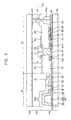
- FIG. 1A is a plan view of an array substrate according to an exemplary embodiment of the present invention.
- FIG. 1B is a perspective view schematically showing a display panel according to an exemplary embodiment of the present invention.
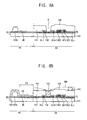
- FIG. 2 is an enlarged plan view of a display panel of FIG. 1 ;
- FIG. 3 is a cross-sectional view of a display panel taken along a line ‘I-I′’ of FIG. 2 ;
- FIGS. 4A to 4E are cross-sectional views showing a method of manufacturing a display panel of FIG. 3 ;
- FIG. 5 is a cross-sectional view of a display panel according to an exemplary embodiment of the present invention.
- FIGS. 6A to 6C are cross-sectional views showing a method of manufacturing a display panel of FIG. 5 ;
- FIG. 7 is a cross-sectional view of a display panel according to an exemplary embodiment of the present invention.
- FIGS. 8A to 8C are cross-sectional views showing a method of manufacturing a display panel of FIG. 7 ;
- FIG. 9 is a cross-sectional view of a display panel according to an exemplary embodiment of the present invention.
- FIGS. 10A to 10B are cross-sectional views showing a method of manufacturing a display panel of FIG. 9 ;
- FIG. 11 is a cross-sectional view of a display panel according to an exemplary embodiment of the present invention.
- FIG. 12 is a cross-sectional view showing a method of manufacturing a display panel of FIG. 11 ;
- FIG. 13 is a cross-sectional view of a display panel in accordance with an exemplary embodiment of the present invention.
- FIGS. 14A to 14C are cross-sectional views showing a method of manufacturing the display panel of FIG. 13 .
- FIG. 1A is a plan view of an array substrate according to an exemplary embodiment of the present invention.
- FIG. 1B is a perspective view schematically showing a display panel according to an exemplary embodiment of the present invention.
- a display panel includes a display substrate 100 a , an opposite substrate 200 facing the display substrate 100 a and a liquid crystal layer (not shown) interposed between the display substrate 100 a and the opposite substrate 200 .
- the display substrate 100 a includes a display area (DA) and a peripheral area (PA) surrounding the display area DA.
- a plurality of gate lines (GL) and a plurality of data lines (DL) crossing the gate lines are formed in the display area DA.
- a plurality of pixel electrodes are formed in the display area DA.
- the peripheral area PA includes a data driving area (DDA), a gate driving area (GDA) and a seal line area (SLA).
- DDA data driving area
- GDA gate driving area
- SLA seal line area
- the data driving area DDA includes input pads receiving driving signals of the display panel and output pads outputting data signals to the data lines.
- the gate driving area GDA includes a gate driving circuit generating gate signals that are applied to the gate lines.
- the seal line area SLA includes a sealant to combine the display substrate 100 a with the opposite substrate 200 .
- the seal line area SLA overlaps the gate driving area GDA.
- the sealant is disposed between the gate driving circuit and a common electrode formed on the opposite substrate 200 , capacitance generated by the gate driving circuit and the common electrode can be reduced.
- FIG. 2 is an enlarged plan view of a display panel of FIG. 1 .
- FIG. 3 is a cross-sectional view taken along a line ‘I-I” of FIG. 2 .
- the display panel includes the display substrate 100 a , the opposite substrate 200 and a liquid crystal layer 300 .
- the opposite substrate 200 includes a common electrode 210 .
- the display substrate 100 a includes a first base substrate 101 .
- the first base substrate 101 includes the display area DA and the peripheral area PA surrounding the display area DA.
- the display area DA includes a transistor layer (TL), color filters 161 , 162 , pixel electrodes PE 1 , PE 2 , a first light blocking member 181 , a spacing part CS 1 and a first transparent member 192 .
- TL transistor layer
- the transistor layer TL includes a gate metal pattern formed on the first base substrate 101 , a gate insulation layer 120 , channel patterns 131 , 132 , a source metal pattern and a passivation layer 150 .
- the gate metal pattern includes a plurality of gate lines GL, gate electrodes GE 1 , GE 2 and a storage line STL.
- the n-th gate line GLn is extended in a first direction.
- the n-th gate line GLn includes the first gate electrode GE 1 of a first transistor TR 1 and the second gate electrode GE 2 of a second transistor TR 2 .
- the storage line STL is formed in parallel with the n-th gate line GLn.
- the gate insulation layer 120 is formed on the gate metal pattern.
- the channel patterns 131 , 132 are formed to correspond to the source metal pattern.
- the first channel pattern 131 is formed on the gate electrodes GE 1 , GE 2 to correspond to source and drain electrodes SE 1 , SE 2 , DE 1 , DE 2
- the second channel pattern 132 is formed to correspond to the data lines DLm ⁇ 2, DLm ⁇ 1, DLm, DLm+1, DLm+2.
- the channel patterns 131 , 132 include an active layer and an ohmic contact layer.
- the source metal pattern includes a plurality of data lines DLm ⁇ 2, DLm ⁇ 1, DLm, DLm+1, DLm+2, the source electrodes SE 1 , SE 2 and the drain electrodes DE 1 , DE 2 .
- the data lines DLm ⁇ 2, DLm ⁇ 1, DLm, DLm+1, DLm+2 are formed in a second direction that crosses the first direction in which the gate lines extend.
- the source electrodes SE 1 , SE 2 extend from the data lines DLm ⁇ 2, DLm ⁇ 1, DLm, DLm+1, DLm+2.
- the source electrodes SE 1 , SE 2 overlap the gate electrodes GE 1 , GE 2 .
- the drain electrodes DE 1 , DE 2 are spaced apart from the source electrode SE 1 , SE 2 and overlap the gate electrodes GE 1 , GE 2 .
- the drain electrodes DE 1 , DE 2 are connected to the pixel electrodes PE 1 , PE 2 through a first contact hole C 1 and a second contact hole C 2 , respectively.
- the passivation layer 150 is formed on the first base substrate 101 where the source metal pattern is formed.
- the passivation layer 150 protects the exposed channel pattern 131 and the source metal patterns of the first and second transistors TR 1 , TR 2 .
- the color filters 161 , 162 are formed in the pixel areas P 1 , P 2 of the first base substrate 101 where the transistor layer TL is formed.
- the color filter 161 includes a first color
- the color filter 162 includes a second color that is different from the first color.
- a boundary area of the color filters 161 , 162 includes a first opening area H 1 to expose the passivation layer 150 .
- portions of the color filters 161 , 162 that are formed between the m-th data line DLm and the n+1-th data line DLm+1 are removed so that the first opening area H 1 is formed.
- the color filters 161 , 162 may further include opening areas that correspond to the first and second contact holes C 1 , C 2 and the storage line STL.
- the pixel electrodes PE 1 , PE 2 are formed in the pixel area P 1 , P 2 .
- the pixel electrodes PE 1 , PE 2 include a first sub electrode 171 and a second sub electrode 172 to divide a domain for arranging liquid crystal molecules.
- the first sub electrode 171 and the second sub electrode 172 can be patterned in a chevron shape.
- the first sub electrode 171 is electrically connected to the drain electrode DE 1 of the first transistor TR 1 through the first contact hole C 1 .
- the second sub electrode 172 is electrically connected to the drain electrode DE 2 of the second transistor TR 2 through the second contact hole C 2 .
- the first light blocking member 181 is formed in the first opening area H 1 .
- the first light blocking member 181 divides the pixel areas P 1 , P 2 where the color filters 161 , 162 are formed.
- the first light blocking member 181 includes a material that can block light.
- the spacing part CS 1 maintains a cell gap (d) between the display substrate 100 a and the opposite substrate 200 .
- the spacing part CS 1 is formed on the color filter 162 corresponding to the n-th gate line GLn.
- the spacing part CS 1 can be disposed in an area corresponding to the gate metal pattern or the source metal pattern.
- the spacing part CS 1 includes a first color pattern 163 a formed on the color filter 162 and a transparent pattern 191 formed on the first color pattern 163 a .
- the first color pattern 163 a includes a third color that is different from the second color of the color filter 162 .
- the first color pattern 163 a is formed of substantially the same material as the color filters 161 , 162 .
- the cell gap d depends on a first thickness (t 1 ) of the color filter 162 , a second thickness (t 2 ) of the first color pattern 163 a and a third thickness (t 3 ) of the transparent pattern 191 .
- first thickness t 1 of the color filter 162 is about 3 ⁇ m
- second thickness t 2 of the first color pattern 163 a is about 3 ⁇ m
- third thickness t 3 of the transparent pattern 191 is about 1 ⁇ m.
- the first transparent member 192 is formed on the first light blocking member 181 to cover the first light blocking member 181 .
- the first transparent member 192 includes substantially the same material as the transparent pattern 191 .
- a fourth thickness t 4 of the first transparent member 192 is thinner than the third thickness t 3 of the transparent pattern 191 .
- the fourth thickness t 4 of the first transparent member 192 is not more than about 1 ⁇ m.
- the fourth thickness t 4 of the first transparent member 192 When the fourth thickness t 4 of the first transparent member 192 is thinner, a height difference between the first transparent member 192 and the color filters 161 , 162 can be reduced so that a spread property of the liquid crystal layer 300 can be improved.
- the spread property refers to a property which allows liquid crystals to move easily between the pixel electrode PE 1 and the pixel electrode PE 2 .
- the first transparent member 192 covers the first light blocking member 181 so that a gas generated from the first light blocking member 181 is blocked by the first transparent member 192 . Thus, an afterimage that may occur by the gas can be prevented.
- the peripheral area PA includes a circuit layer CL, a second color pattern 163 b , a second light blocking member 183 , a contact electrode CE and a second transparent member 193 .
- the circuit layer CL includes a metal pattern (ME), the gate insulation layer 120 and the passivation layer 150 to form the gate driving circuit and an electrostatic prevention circuit.
- the metal pattern ME includes the gate metal pattern and the source metal pattern.
- the second color pattern 163 b is formed on the circuit layer CL of the peripheral area PA.
- the second color pattern 163 b includes substantially the same material as the color filters 161 , 162 .
- the second light blocking member 183 is formed in the peripheral area PA where the second color pattern 163 b is formed.
- the second light blocking member 183 includes substantially the same material as the first light blocking member 181 .
- the first and second light blocking members 181 , 183 can be manufactured by a same manufacturing process.
- the second light blocking member 183 includes a second opening area H 2 corresponding to the metal pattern ME.
- the metal pattern ME is electrically connected to the contact electrode CE through the second opening area H 2 .
- the second transparent member 193 is formed on the second light blocking member 183 of the peripheral area PA.
- the second transparent member 193 includes a protrusion 193 a formed in an area corresponding to the second color pattern 163 b .
- the second transparent member 193 covers the second light blocking member 183 so that a gas generated from the second light blocking member 183 is blocked by the second transparent member 193 .
- a fifth thickness t 5 of the second transparent member 193 is thinner than the thickness t 3 of the transparent pattern 191 . In an exemplary embodiment, the fifth thickness t 5 of the second transparent member 193 is not more than about 1 ⁇ m.
- a protrusion part (CS 2 ) is formed in the peripheral area PA.
- the protrusion part CS 2 includes the second color pattern 163 b , the second light blocking member 183 and the second transparent member 193 .
- a thickness of the protrusion part CS 2 is thinner than a combined thickness of the color filter 162 , the first color pattern 163 a and the transparent pattern 191 .
- the protrusion part CS 2 can reduce a volume of the liquid crystal layer 300 to be filled so that a filling property of the liquid crystal layer 300 can be improved.
- FIGS. 4A to 4E are cross-sectional views showing a method of manufacturing a display panel of FIG. 3 .
- the display area DA of the base substrate 101 includes the transistor layer TL, and the peripheral area PA of the base substrate 101 includes the circuit layer CL.
- a gate metal layer is formed on the base substrate 101 .
- the gate metal pattern is formed by patterning the gate metal layer.
- the gate metal pattern includes the n-th gate line GLn, the gate electrodes GE 1 , GE 2 , the storage line STL and the metal pattern ME of the peripheral area PA.
- the gate insulation layer 120 is formed on the base substrate 101 where the gate metal pattern is formed.
- a channel layer and a source metal layer are formed on the base substrate 101 where the gate insulation layer 120 is formed.
- the channel patterns 131 , 132 may be formed on the gate insulation layer 120 .
- the source metal pattern includes the data lines DLm ⁇ 1, DLm, the source electrodes SE 1 , SE 2 and the drain electrodes DE 1 , DE 2 .
- the first channel pattern 131 is formed behind/under the source electrodes SE 1 , SE 2 and the drain electrodes DE 1 , DE 2 .
- the second channel pattern 132 is formed behind/under the data lines DLm ⁇ 1, DLm.
- the source metal pattern may further include a metal pattern for the gate driving circuit and the electrostatic prevention circuit in the peripheral area PA.
- the passivation layer 150 is formed on the base substrate 101 where the source metal pattern is formed.
- the color filters 161 , 162 , the first color pattern 163 a and the second color pattern 163 b are formed on the base substrate 101 where the transistor layer TL and the circuit layer CL are formed.
- the color filter 161 including the first color is formed in the first pixel area P 1 .
- the color filter 162 including the second color is formed in the second pixel area P 2 .
- a color photo-resist layer including a third color is formed and patterned.
- the first color pattern 163 a is formed in the display area DA
- the second color pattern 163 b is formed in the peripheral area PA.
- the first opening area H 1 is formed in the boundary area between the pixel areas P 1 , P 2 where the color filters 161 , 162 are formed.
- the opening area H 1 is extended in parallel with an extended direction of the data lines DLm ⁇ 1, DLm.
- the color filters 161 , 162 may include opening areas to expose the passivation layer 150 corresponding to the first and second contact holes C 1 , C 2 .
- a light blocking layer 180 is formed on the base substrate 101 where the color filters 161 , 162 , the first color pattern 163 a and the second color pattern 163 b are formed.
- the first light blocking member 181 is formed in the display area DA and the second light blocking member 183 is formed in the peripheral area PA by patterning the light blocking layer 180 .
- the light blocking layer 180 may have a thickness to form the first light blocking member 181 in the first opening area H 1 of the display area DA.
- the second light blocking member 183 includes the second opening area H 2 corresponding to an area where the metal pattern ME and contact electrode CE are formed.
- a transparent conductive layer 170 is formed on the base substrate 101 where the first and second light blocking members 181 , 183 are formed.
- the transparent conductive layer 170 is patterned so that the pixel electrodes PE 1 , PE 2 are formed in the display area DA and the contact electrode CE is formed in the peripheral area PA.
- the pixel electrodes PE 1 , PE 2 are formed in the first and second pixel areas P 1 , P 2 , respectively.
- the contact electrode CE is connected to the metal pattern ME of the circuit area CA through the second opening area H 2 .
- a covering layer 190 is formed on the base substrate 101 where the pixel electrodes PE 1 , PE 2 and the contact electrode CE are formed.
- the covering layer 190 includes, for example, a transparent material.
- the transparent material may forms part or all of a spacing part in a liquid crystal display device. Since the covering layer 190 is formed on the first color pattern 163 a , the covering layer 190 may have a thinner thickness due to the second thickness t 2 of the first color pattern 163 a .
- a thickness of the first color pattern 163 a is about 3 ⁇ m so that a thickness of the transparent pattern 191 formed by the covering layer 190 is about 1 ⁇ m.
- the thickness of the transparent pattern 191 is about 4 ⁇ m.
- the covering layer 190 is patterned by using a mask 510 including a transmissive portion 511 , a light blocking portion 512 and a slit portion 513 .
- the transmissive portion 511 corresponds to the first color pattern 163 a
- the slit portion 513 corresponds to portions of the display and the peripheral areas DA, PA.
- the light blocking portion 512 corresponds to an area where the covering layer 190 is not formed.
- the transmissive portion 511 may be formed in an area corresponding to the second color pattern 163 b.
- the covering layer 190 includes the first transparent member 192 formed on the first light blocking member 181 and the second transparent member 193 in the peripheral area PA.
- the second transparent member 193 may further include the protrusion 193 a corresponding to the second color pattern 163 b.
- the first and second transparent members 192 , 193 patterned by the slit portion 513 may have thinner thicknesses than the thickness of the transparent pattern 191 patterned by the transmissive portion 511 .
- the thickness of the first transparent member 192 is thinner, a spread property of the liquid crystal layer 300 can be improved.
- FIG. 5 is a cross-sectional view of a display panel according to an exemplary embodiment of the present invention.
- the display panel includes a display substrate 100 b , the opposite substrate 200 and the liquid crystal layer 300 .
- the display substrate 100 b includes the base substrate 101 having the display area DA and the peripheral area PA.
- the display area DA includes the transistor layer TL, the color filters 161 , 162 , the pixel electrodes PE 1 , PE 2 , the first light blocking member 181 , the spacing part CS 1 and the first transparent member 192 .
- the peripheral area PA includes the circuit layer CL, the second color pattern 163 b , the second light blocking member 183 , the contact electrode CE and the second transparent member 193 .
- the spacing part CS 1 includes the first color pattern 163 a and the transparent pattern 191 .
- the first color pattern 163 a is formed on the transistor layer TL and corresponds to the n-th gate line GLn.
- the color filter 162 is formed on the first color pattern 163 a and corresponds to the gate metal pattern and the source metal pattern.
- the transparent pattern 191 includes substantially the same material as the first and second transparent members 192 , 193 .
- the transparent pattern 191 is formed on the color filter 162 where the first color pattern 163 a is formed.
- An end portion of the transparent pattern 191 is in contact with the opposite substrate 200 and to maintain the cell gap d of the liquid crystal layer 300 .
- the cell gap d includes part of a thickness t 2 of the color filter 162 and a thickness t 3 of the transparent pattern 191 .
- the thickness t 1 of the first color pattern 163 a is about 3 ⁇ m
- the thickness t 2 of the color filter 162 formed on the first color pattern 163 a is about 2 ⁇ m
- the thickness t 3 of the transparent pattern 191 is about 2-3 ⁇ m.
- a thickness t 4 of the first transparent member 192 and a thickness t 5 of the second transparent member 193 are thinner than the thickness t 3 of the transparent pattern 191 .
- the thickness t 4 of the first transparent member 192 is not more than about 2 ⁇ m.
- FIGS. 6A to 6C are cross-sectional views showing a method of manufacturing a display panel of FIG. 5 .
- the transistor layer TL is formed in the display area DA of the base substrate 101 , and the circuit layer CL is formed in the peripheral area PA.
- the first color pattern 163 a is formed in the display area DA of the base substrate 101 where the transistor layer TL and the circuit layer CL are formed.
- the first color pattern 163 a is formed by using a color photo-resist layer having a third color.
- the second color pattern 163 b is formed in the peripheral area PA.
- the first color pattern 163 a is formed to correspond to an area where the n-th gate line GLn is formed.
- the first color pattern 163 a is formed to correspond to an area where the gate metal pattern and the source metal pattern are formed.
- the color filter 161 having the first color and the color filter 162 having the second color are formed in the first and second pixel areas, respectively.
- the color filter 162 is formed on the first color pattern 163 a.
- the first opening area H 1 is formed in a boundary area between the pixel areas P 1 , P 2 where the color filters 161 , 162 are formed.
- the color filters 161 , 162 may include opening areas to expose the passivation layer 150 corresponding to the first and second contact holes C 1 , C 2 .
- the first light blocking member 181 and the second light blocking member 183 are formed on the base substrate 101 where the color filters 161 , 162 , the first color pattern 163 a and the second color pattern 163 b are formed.
- the first light blocking member 181 is formed in the first opening area H 1 of the display area DA.
- the second light blocking member 183 includes the second opening area H 2 corresponding to an area where the metal pattern ME and the contact electrode CE are formed.
- the pixel electrodes PE 1 , PE 2 and the contact electrode CE are formed on the base substrate 101 where the first and second light blocking members 181 , 183 are formed.
- the pixel electrodes PE 1 , PE 2 are formed in the first and second areas P 1 , P 2 , respectively.
- the contact electrode CE is connected to the metal pattern of the circuit area CA through the second opening area H 2 .
- the covering layer 190 is formed on the base substrate 101 where the pixel electrodes PE 1 , PE 2 and the contact electrode CE are formed.
- the covering layer 190 may include, for example, a transparent photo-sensitive material. Since the covering layer 190 is formed on the first color pattern 163 a and the color filter 162 , the covering layer 190 may have a thinner thickness due to a thickness of the first color pattern 163 a and the color filter 162 . In an exemplary embodiment, when the cell gap d is about 4 ⁇ m, a thickness of the first color pattern 163 a t 1 is about 3 ⁇ m and a thickness t 2 of the color filter 162 overlapped with the first color pattern 163 a is about 2 ⁇ m so that a thickness t 3 of the transparent pattern 191 formed by the covering layer 190 is about 2-3 ⁇ m.
- the thickness of the transparent pattern 191 is about 4 ⁇ m. In an exemplary embodiment, the thickness of the transparent pattern 191 is about 2-3 ⁇ m when the color pattern 163 a is included.
- the covering layer 190 is patterned by using a mask 610 including a transmissive portion 611 , a light blocking portion 612 and a slit portion 613 .
- the transmissive portion 611 corresponds to the first color pattern 163 a
- the slit portion 613 corresponds to parts of the display and the peripheral areas DA, PA.
- the light blocking portion 612 corresponds to an area where the covering layer 190 is not formed.
- the transmissive portion 611 may further be formed in an area corresponding to the second color pattern 163 b.
- the covering layer 190 includes the first transparent member 192 formed on the first light blocking member 181 and the second transparent member 193 in the peripheral area PA.
- the second transparent member 193 may further include the protrusion 193 a corresponding to the second color pattern 163 b.
- the first and second transparent members 192 , 193 patterned by the slit portion 613 may have thinner thicknesses than the thickness of the transparent pattern 191 patterned by the transmissive portion 611 .
- a thickness of the first transparent member 192 is thinner, a spread property of the liquid crystal layer 300 can be improved.
- FIG. 7 is a cross-sectional view of a display panel according to an exemplary embodiment of the present invention.
- the display panel includes a display substrate 100 c , the opposite substrate 200 and the liquid crystal layer 300 .
- the display substrate 100 c includes the base substrate 101 having the display area DA and the peripheral area PA.
- the display area DA includes the transistor layer TL, the color filters 161 , 162 , the pixel electrodes PE 1 , PE 2 , the first light blocking member 181 , the spacing part CS 1 and the first transparent member 192 .
- the peripheral area PA includes the circuit layer CL, the second color pattern 163 b , the second light blocking member 183 , the contact electrode CE and the second transparent member 193 .
- the spacing part CS 1 includes a light blocking pattern 182 and the transparent pattern 191 .
- the light blocking pattern 182 is formed on the color filter 162 corresponding to the n-th gate line GLn. In an exemplary embodiment, the light blocking pattern 182 is formed on the color filter 162 corresponding to the gate metal pattern and the source metal pattern.
- the light blocking pattern 182 may include substantially the same material as the first and second light blocking members 181 , 183 .
- the light blocking pattern 182 may be manufactured using the same process used in manufacturing the first and second light blocking members 181 , 183 .
- the transparent pattern 191 may include substantially the same material as the first and second transparent members 192 , 193 .
- the transparent pattern 191 is formed on the light blocking pattern 182 .
- An end portion of the transparent pattern 191 is in contact with a surface of the opposite substrate 200 and forms the cell gap d of the liquid crystal layer 300 .
- the cell gap d includes a thickness of the light blocking member 182 and a thickness of the transparent pattern 191 .
- the thickness t 1 of the color filter 162 is about 3 ⁇ m
- the thickness of the light blocking pattern t 2 182 is about 2 ⁇ m
- the thickness t 3 of the transparent pattern 191 is about 2 ⁇ m.
- the thickness of the first transparent member 192 and the thickness of the second transparent member 193 are thinner than the thickness of the transparent pattern 191 .
- the thickness of the first transparent member 192 is not more than about 2 ⁇ m.
- the thickness of the first transparent member 192 is thinner, a spread property of the liquid crystal layer 300 can be improved.
- the light blocking pattern 182 includes a material having a higher optical density, the thickness of the first transparent member 192 formed on the first light blocking pattern 181 can be reduced.
- FIGS. 8A to 8C are cross-sectional views showing a method of manufacturing a display panel of FIG. 7 .
- the transistor layer TL is formed in the display area DA of the base substrate 101 and the circuit layer CL is formed in the peripheral area PA.
- the color filters 161 , 162 are formed on the transistor layer TL of the display area DA.
- the color pattern 163 b is formed on the circuit layer CL of the peripheral area PA.
- the first opening area H 1 is formed in a boundary area of the color filters 161 , 162 .
- the color filters 161 , 162 may include opening areas to expose the passivation layer 150 corresponding to the first and second contact holes C 1 , C 2 .
- the light blocking layer 180 is formed on the base substrate 101 where the color filters 161 , 162 and the color pattern 163 b are formed.
- the first light blocking member 181 of the display area DA and the second light blocking pattern 182 are formed by patterning the light blocking layer 180 .
- the first light blocking member 181 is formed in the first opening area H 1 .
- the light blocking pattern 182 is formed on the color filter 162 .
- the second light blocking member 183 is formed in the peripheral area PA, and the second opening area H 2 is formed in an area corresponding to the metal pattern ME of the circuit area CA.
- the covering layer 190 is formed on the base substrate 101 where the light blocking pattern 182 , the first light blocking member 181 and the second light blocking member 183 are formed.
- the covering layer 190 includes a transparent photo-sensitive material.
- the covering layer 190 may have a thinner thickness due to the thickness of the light blocking pattern 182 .
- a thickness t 1 of the color filter 162 is about 3 ⁇ m and a thickness t 2 of the light blocking pattern 182 formed on the color filter 162 is about 2 ⁇ m, so that a thickness t 3 of the transparent pattern 191 formed by the covering layer 190 is about 2 ⁇ m.
- the thickness of the transparent pattern 191 is about 4 ⁇ m.
- the thickness of the transparent pattern 191 is about 2 ⁇ m when formed on the light blocking pattern 182 .
- the covering layer 190 is patterned by using a mask 710 including a transmissive portion 711 , a light blocking portion 712 and a slit portion 713 .
- the transmissive portion 711 corresponds to the light blocking pattern 182
- the slit portion 713 corresponds to parts of the display and the peripheral areas DA, PA.
- the light blocking portion 712 corresponds to an area where the covering layer 190 is not formed.
- the transmissive portion 711 may further be formed in an area corresponding to the second color pattern 163 b.
- the covering layer 190 includes the transparent pattern 191 formed on the first light blocking member 182 , the first transparent member 192 formed on the first light blocking member 181 , and the second transparent member 193 having the protrusion 193 a in the peripheral area PA.
- the first and second transparent members 192 , 193 patterned by the slit portion 713 may have thinner thicknesses than the thickness of the transparent pattern 191 patterned by the transmissive portion 711 .
- a thickness of the first transparent member 192 is thinner, a spread property of the liquid crystal layer 300 can be improved.
- FIG. 9 is a cross-sectional view of a display panel according to an exemplary embodiment of the present invention.
- the display panel includes a display substrate 100 d , the opposite substrate 200 and the liquid crystal layer 300 .
- the display substrate 100 d includes the base substrate 101 having the display area DA and the peripheral area PA.
- the display area DA includes the transistor layer TL, the color filters 161 , 162 , the pixel electrodes PE 1 , PE 2 , the first light blocking member 181 , and the spacing part CS 1 .
- the peripheral area PA includes the circuit layer CL, the second color pattern 163 b , the contact electrode CE and the second light blocking member 183 .
- the protrusion part (CS 2 ) including the second color pattern 163 b and the second light blocking member 183 is formed in the peripheral area PA.
- the spacing part CS 1 includes the first color pattern 163 a and the light blocking pattern 182 .
- the first color pattern 163 a is formed on the transistor layer TL corresponding to the n-th gate line GLn.
- the first color pattern 163 a is formed on the transistor layer TL corresponding to the gate metal pattern and the source metal pattern.
- the first color pattern 163 a includes a different color from the color filter 162 .
- the light blocking pattern 182 includes substantially the same material as the first and second light blocking members 181 , 183 .
- the light blocking pattern 182 is formed on the color filter 162 corresponding to where the first color pattern 163 a is formed. An end portion of the light blocking pattern 182 is in contact with the opposite substrate 200 and maintains the cell gap d of the liquid crystal layer 300 .
- the cell gap d includes part of a thickness t 2 of the color filter 162 and a thickness t 3 of the light blocking pattern 182 .
- the thickness t 1 of the first color pattern 163 a is about 3 ⁇ m
- the thickness t 2 of the color filter 162 formed on the first color pattern 163 a is about 2 ⁇ m
- the thickness t 3 of the light blocking pattern 182 is about 2-3 ⁇ m.
- the second light blocking member 183 is formed in the peripheral area PA where the second color pattern 163 b and the contact electrode CE of the circuit area CA are formed.
- the second light blocking member 183 is in contact with the contact electrode CE. Since the second light blocking member 183 covers the metal pattern ME of the circuit area CA and the contact electrode CE, light leakage that is reflected by the metal pattern ME and the contact electrode CE can be prevented.
- FIGS. 10A to 10C are cross-sectional views showing a method of manufacturing a display panel of FIG. 9 .
- the transistor layer TL is formed in the display area DA of the base substrate 101 , and the circuit layer CL is formed in the peripheral area PA.
- the first color pattern 163 a of the display area DA and the second color pattern 163 b of the peripheral area PA are formed by using a color photo-resist layer having a third color.
- the first color pattern 163 a is formed in an area corresponding to the n-th gate line GLn. In an exemplary embodiment, the first color pattern 163 a is formed in an area corresponding to the gate metal pattern and the source metal pattern.
- the color filters 161 , 162 having first and second colors are formed in the first pixel area and the second pixel area, respectively.
- the color filter 162 is formed on the first color pattern 163 a.
- the first opening area H 1 is formed in a boundary area between the pixel areas P 1 , P 2 where the color filters 161 , 162 are formed.
- the color filters 161 , 162 may include opening areas to expose the passivation layer 150 corresponding to the first and second contact holes C 1 , C 2 .
- the first contact hole, the second contact hole and a third contact hole to expose the drain electrodes DE 1 , DE 2 and the metal pattern ME are formed by etching the base substrate 101 where the first and second color patterns 163 a , 163 b and the color filters 161 , 162 are formed.
- the transparent conductive layer 170 is formed on the base substrate 101 where the first, second and third contact holes C 1 , C 2 , C 3 are formed.
- a negative type photo-resist pattern PR is formed on the base substrate 101 where the transparent conductive layer 170 is formed.
- the pixel electrodes PE 1 , PE 2 of the display area DA and the contact electrode CE of the circuit area CA of the peripheral area PA are formed by patterning the transparent conductive layer 170 .
- the light blocking layer 180 is formed on the base substrate 101 where the pixel electrodes PE 1 , PE 2 and the contact electrode CE are formed.
- a mask 810 including a transmissive portion 811 and light blocking portion 812 is disposed on the base substrate 101 where the light blocking layer 180 is formed.
- the transmissive portion 811 corresponds to an area where the light blocking layer 180 remains. In an exemplary embodiment, the transmissive portion 811 corresponds to the light blocking pattern 182 , the first light blocking member 181 and the second light blocking member 183 .
- the light blocking layer 180 is patterned by the mask 810 so that the first light blocking member 181 and the light blocking pattern 182 of the display area DA and the second light blocking member 183 of the peripheral area PA are formed.
- a thickness t 1 of the first color pattern 163 a is about 3 ⁇ m and a thickness t 2 of the color filter 162 overlapped with the first color pattern 163 a is about 2 ⁇ m so that a thickness of the light blocking pattern 182 is about 2-3 ⁇ m.
- a spread property of the liquid crystal layer 300 can be improved.
- FIG. 11 is a cross-sectional view of a display panel according to an exemplary embodiment of the present invention.
- the display panel includes a display substrate 100 e , the opposite substrate 200 and the liquid crystal layer 300 .
- the display substrate 100 e includes the base substrate 101 having the display area DA and the peripheral area PA.
- the display area DA includes the transistor layer TL, the color filters 161 , 162 , the pixel electrodes PE 1 , PE 2 , the first light blocking member 181 and the light blocking pattern 182 .
- the peripheral area PA includes the circuit layer CL, the second color pattern 163 b , the contact electrode CE and the second light blocking member 183 .
- the protrusion part CS 2 including the second color pattern 163 b and the second light blocking member 183 is formed in the peripheral area PA.
- the light blocking pattern 182 is formed on the color filter 162 and corresponds to an area where the gate metal pattern is overlapped with the source metal pattern.
- the light blocking pattern is disposed in an area where the n-th gate line GLn crosses the data lines DLm ⁇ 2, DLm ⁇ 1, DLm, DLm+1, DLm+2, or the first and second transistors TR 1 , TR 2 are formed.
- the cell gap d includes a part of the thickness t 2 of the color filter 162 and a thickness t 3 of the light blocking pattern 182 .
- the thickness t 1 of the gate and source metal pattern is about 3 ⁇ m and the thickness t 2 of the color filter 162 is about 3 ⁇ m, and the thickness t 3 of the light blocking pattern 182 is about 3 ⁇ m.
- FIG. 12 is a cross-sectional view showing a method of manufacturing a display panel of FIG. 11 .
- the transistor layer TL is formed in the display area DA of the base substrate 101 , and the circuit layer CL is formed in the peripheral area PA.
- the color filters 161 , 162 are formed on the transistor layer TL.
- the color pattern 163 b is formed on the circuit layer CL.
- the first, second and third contact holes C 1 , C 2 , C 3 to expose the drain electrodes DE 1 , DE 2 and the metal pattern ME are formed by etching the base substrate 101 where the color pattern 163 b and the color filters 161 , 162 are formed.
- the pixel electrodes PE 1 , PE 2 and the contact electrode CE are formed on the base substrate 101 where the first, second, third contact holes C 1 , C 2 , C 3 are formed.
- the light blocking layer 180 is formed on the base substrate 101 having the pixel electrodes PE 1 , PE 2 and the contact electrode CE.
- a mask 910 including a transmissive portion 911 and a light blocking portion 912 is disposed on the base substrate where the light blocking layer 180 is formed.
- the transmissive portion 911 corresponds to an area where the light blocking layer 180 remains.
- the transmissive portion 911 corresponds to the light blocking pattern 182 , the first light blocking member 181 and the second light blocking member 183 .
- the light blocking layer 180 is patterned by the mask 910 so that the first light blocking member 181 and the light blocking pattern 182 of the display area DA and the second light blocking member 183 of the peripheral area PA are formed.
- a thickness of the gate and source metal pattern is about 1 ⁇ m and a thickness of the color filter 162 is about 3 ⁇ m so that a thickness of the light blocking pattern 182 is about 3 ⁇ m.
- a spread property of the liquid crystal layer 300 can be improved.
- FIG. 13 is a cross-sectional view of a display panel in accordance with an exemplary embodiment of the present invention.
- the display panel of the present embodiment is substantially the same as the display panel of FIGS. 1 to 4E except with respect to, for example, a spacing part, a transparent member, a pixel electrode and a contact electrode. Thus, any repetitive explanation concerning the above element will be omitted.
- the display panel includes the display substrate 100 f , the opposite substrate 200 and a liquid crystal layer 300 .
- Color filters 161 and 162 are formed in pixel areas P 1 and P 2 of a first base substrate 101 where a transistor layer TL is formed.
- a first light blocking member 181 is formed in a first opening area H 1 .
- the first light blocking member 181 divides the pixel areas P 1 and P 2 where the color filters 161 and 162 are formed.
- the spacing part CS 1 maintains a cell gap d between the display substrate 100 a and the opposite substrate 200 .
- the spacing part CS 1 is formed on the color filter 162 corresponding to the n-th gate line GLn.
- the spacing part CS 1 can be disposed in an area corresponding to the gate metal pattern or the source metal pattern.
- the spacing part CS 1 includes a transparent pattern 291 and a spacing blocking pattern 181 a instead of the first color pattern 163 a (shown in FIG. 3 ).
- the spacing blocking member 181 a is formed on the color filter 162
- the transparent pattern 291 is formed on the spacing blocking pattern 181 a.
- a first transparent member 292 is formed on the first light blocking member 181 to cover the first light blocking member 181 and the color filters 161 and 162 .
- the first transparent member 292 is formed from the same layer as the transparent pattern 291 .
- a fourth thickness t 4 of the first transparent member 292 is thinner than the third thickness t 3 of the transparent pattern 291 .
- the first transparent member 292 is formed on the first light blocking member 181 and the color filters 161 and 162 to prevent the first light blocking member 181 and the color filters 161 and 162 from being exposed. Thus, an afterimage that may occur by gas generated from the first light blocking member 181 can be prevented.
- the first transparent member 292 is extended towards the color filters 161 and 162 to prevent the color filters 161 and 162 from being exposed to a liquid crystal layer 300 .
- impurities from the color filters 161 and 162 are blocked by the first transparent member 292 to protect the liquid crystal layer 300 .
- the second transparent member 293 is formed on the second light blocking member 183 of the peripheral area PA.
- a contact electrode CE is electrically connected to a metal pattern ME through a second contact hole H 2 that is formed through the second transparent member 293 , the second light blocking member 183 , the passivation layer 150 and the gate insulating layer 120 .
- Pixel electrodes PE 1 and PE 2 are formed on the first transparent member 292 in pixel regions P 1 and P 2 .
- FIGS. 14A to 14C are cross-sectional views showing a method of manufacturing the display panel of FIG. 13 .
- FIG. 14A is a cross-sectional view illustrating forming the first light blocking member, the second light blocking member and the spacing blocking pattern shown in FIG. 13 .
- a gate metal pattern, the gate insulating layer 120 , a source metal pattern, the passivation layer 150 and the color filters 161 and 162 are formed on the base substrate 101 .
- the first color pattern 163 a (shown in FIG. 4C ) is omitted.
- a light blocking layer 180 is formed on the base substrate 101 where the color filters 161 and 162 and the second color pattern 163 b are formed.
- the first light blocking member 181 and the spacing blocking pattern 181 a are formed in the display area DA, and the second light blocking member 183 is formed in the peripheral area PA by patterning the light blocking layer 180 .
- the first light blocking member 181 is formed in the first contact hole H 1 in the display area DA, and the spacing blocking pattern 181 a is formed on the color filter 162 .
- FIG. 14B is a cross-sectional view illustrating a transparent pattern and a first transparent member on the substrate shown in FIG. 14A .
- a covering layer 290 is formed on the base substrate 101 where the first and second light blocking members 181 and 182 and the spacing blocking pattern 181 a are formed.
- the covering layer 290 is patterned by using a mask 610 including a transmissive portion 611 , a light blocking portion 614 and a slit portion 613 .
- the transmissive portion 611 corresponds to the spacing blocking pattern 181 a
- the light blocking portion 614 corresponds to the second contact hole H 2 .
- the slit portion 613 corresponds to a remainder of the base substrate 101 .
- the transparent pattern 291 and the first transparent member 292 are formed.
- FIG. 14C is a cross-sectional view illustrating forming a pixel electrode and a contact electrode on the substrate shown in FIG. 14B .
- a transparent conductive layer 270 is formed on the base substrate 101 where the transparent pattern 291 and the first transparent member 292 are formed.
- the transparent conductive layer 270 is patterned so that the pixel electrodes PE 1 and PE 2 are formed in the display area DA and the contact electrode CE is formed in the peripheral area PA.
Landscapes
- Physics & Mathematics (AREA)
- Nonlinear Science (AREA)
- Mathematical Physics (AREA)
- Chemical & Material Sciences (AREA)
- Crystallography & Structural Chemistry (AREA)
- General Physics & Mathematics (AREA)
- Optics & Photonics (AREA)
- Liquid Crystal (AREA)
- Engineering & Computer Science (AREA)
- Microelectronics & Electronic Packaging (AREA)
- Devices For Indicating Variable Information By Combining Individual Elements (AREA)
Abstract
Description
Claims (20)
Applications Claiming Priority (3)
| Application Number | Priority Date | Filing Date | Title |
|---|---|---|---|
| KR2008-90893 | 2008-09-17 | ||
| KR1020080090893A KR101513645B1 (en) | 2008-09-17 | 2008-09-17 | Array substrate and manufacturing method thereof |
| KR10-2008-0090893 | 2008-09-17 |
Publications (2)
| Publication Number | Publication Date |
|---|---|
| US20100065850A1 US20100065850A1 (en) | 2010-03-18 |
| US8071406B2 true US8071406B2 (en) | 2011-12-06 |
Family
ID=42006414
Family Applications (1)
| Application Number | Title | Priority Date | Filing Date |
|---|---|---|---|
| US12/425,744 Active 2029-11-17 US8071406B2 (en) | 2008-09-17 | 2009-04-17 | Array substrate and method of manufacturing the same |
Country Status (3)
| Country | Link |
|---|---|
| US (1) | US8071406B2 (en) |
| JP (1) | JP5536370B2 (en) |
| KR (1) | KR101513645B1 (en) |
Families Citing this family (12)
| Publication number | Priority date | Publication date | Assignee | Title |
|---|---|---|---|---|
| US8077275B2 (en) * | 2008-05-09 | 2011-12-13 | Samsung Electronics Co., Ltd. | Display substrate and a method of manufacturing the same |
| KR101581774B1 (en) * | 2009-06-18 | 2016-01-04 | 삼성디스플레이 주식회사 | Liquid crystal display and manufacturing method thereof |
| KR101878458B1 (en) * | 2011-07-08 | 2018-07-16 | 삼성디스플레이 주식회사 | Display substrate andmethod for manufacturing the same |
| KR102032962B1 (en) | 2012-10-26 | 2019-10-17 | 삼성디스플레이 주식회사 | Thin film transistor array substrate and manufacturing method thereof |
| KR102185102B1 (en) * | 2014-01-10 | 2020-12-02 | 삼성디스플레이 주식회사 | Array substrate, liquid crystal display panel having the same and method of manufacturing the same |
| JP6350016B2 (en) * | 2014-06-24 | 2018-07-04 | セイコーエプソン株式会社 | Display device and manufacturing method of display device |
| KR102540811B1 (en) * | 2015-12-04 | 2023-06-07 | 삼성디스플레이 주식회사 | Display device |
| KR102376292B1 (en) * | 2017-07-26 | 2022-03-18 | 삼성디스플레이 주식회사 | Display device |
| KR102569312B1 (en) * | 2018-06-07 | 2023-08-22 | 삼성디스플레이 주식회사 | Display device |
| CN109407413A (en) * | 2018-11-12 | 2019-03-01 | 惠科股份有限公司 | Display panel, display device and manufacturing photomask thereof |
| CN113608390B (en) * | 2021-07-15 | 2022-04-19 | 惠科股份有限公司 | Array substrate and display panel |
| KR20230089603A (en) * | 2021-12-13 | 2023-06-21 | 삼성디스플레이 주식회사 | Display device and method of manufacturing for the same |
Citations (6)
| Publication number | Priority date | Publication date | Assignee | Title |
|---|---|---|---|---|
| US6749975B2 (en) * | 2002-11-20 | 2004-06-15 | Hannstar Display Corporation | Method of utilizing color photoresist to form black matrix and spacers on a control circuit substrate |
| US20050117082A1 (en) * | 2000-05-31 | 2005-06-02 | Nec Lcd Technologies, Ltd. | Color liquid crystal display device and manufacturing method of the same |
| KR20060086644A (en) | 2005-01-27 | 2006-08-01 | 비오이 하이디스 테크놀로지 주식회사 | Manufacturing method of color filter substrate of liquid crystal panel |
| KR20070035145A (en) | 2005-09-27 | 2007-03-30 | 삼성전자주식회사 | Color filter substrate for liquid crystal display device and manufacturing method thereof |
| KR20080032852A (en) | 2006-10-11 | 2008-04-16 | 삼성전자주식회사 | Display substrate and manufacturing method thereof |
| US20090268117A1 (en) * | 1995-10-12 | 2009-10-29 | Semiconductor Energy Laboratory Co., Ltd. | Liquid Crystal Display Device |
Family Cites Families (10)
| Publication number | Priority date | Publication date | Assignee | Title |
|---|---|---|---|---|
| JPH086006A (en) * | 1994-06-16 | 1996-01-12 | Hitachi Ltd | Liquid crystal display device and manufacturing method thereof |
| JPH09105953A (en) * | 1995-10-12 | 1997-04-22 | Semiconductor Energy Lab Co Ltd | Liquid crystal display device |
| JP3726652B2 (en) * | 2000-07-27 | 2005-12-14 | Jsr株式会社 | Radiation-sensitive composition, spacer, and color liquid crystal display device |
| JP2002090720A (en) * | 2000-09-18 | 2002-03-27 | Toshiba Corp | Liquid crystal display |
| JP2002277865A (en) * | 2001-03-21 | 2002-09-25 | Matsushita Electric Ind Co Ltd | Liquid crystal display device and manufacturing method thereof |
| JP2003029269A (en) * | 2001-07-17 | 2003-01-29 | Toshiba Corp | Liquid crystal display device and method of manufacturing liquid crystal display device |
| JP2003172946A (en) * | 2001-09-28 | 2003-06-20 | Fujitsu Display Technologies Corp | Liquid crystal display device substrate and liquid crystal display device using the same |
| KR100772940B1 (en) * | 2001-12-05 | 2007-11-02 | 엘지.필립스 엘시디 주식회사 | Color filter substrate for liquid crystal display device and manufacturing method thereof |
| JP2004219529A (en) * | 2003-01-10 | 2004-08-05 | Toshiba Matsushita Display Technology Co Ltd | Liquid crystal display device and method for manufacturing the same |
| JP4818065B2 (en) * | 2006-02-03 | 2011-11-16 | 東芝モバイルディスプレイ株式会社 | Liquid crystal display |
-
2008
- 2008-09-17 KR KR1020080090893A patent/KR101513645B1/en active Active
-
2009
- 2009-04-17 US US12/425,744 patent/US8071406B2/en active Active
- 2009-06-12 JP JP2009141460A patent/JP5536370B2/en active Active
Patent Citations (6)
| Publication number | Priority date | Publication date | Assignee | Title |
|---|---|---|---|---|
| US20090268117A1 (en) * | 1995-10-12 | 2009-10-29 | Semiconductor Energy Laboratory Co., Ltd. | Liquid Crystal Display Device |
| US20050117082A1 (en) * | 2000-05-31 | 2005-06-02 | Nec Lcd Technologies, Ltd. | Color liquid crystal display device and manufacturing method of the same |
| US6749975B2 (en) * | 2002-11-20 | 2004-06-15 | Hannstar Display Corporation | Method of utilizing color photoresist to form black matrix and spacers on a control circuit substrate |
| KR20060086644A (en) | 2005-01-27 | 2006-08-01 | 비오이 하이디스 테크놀로지 주식회사 | Manufacturing method of color filter substrate of liquid crystal panel |
| KR20070035145A (en) | 2005-09-27 | 2007-03-30 | 삼성전자주식회사 | Color filter substrate for liquid crystal display device and manufacturing method thereof |
| KR20080032852A (en) | 2006-10-11 | 2008-04-16 | 삼성전자주식회사 | Display substrate and manufacturing method thereof |
Also Published As
| Publication number | Publication date |
|---|---|
| JP5536370B2 (en) | 2014-07-02 |
| US20100065850A1 (en) | 2010-03-18 |
| JP2010072621A (en) | 2010-04-02 |
| KR20100031976A (en) | 2010-03-25 |
| KR101513645B1 (en) | 2015-04-21 |
Similar Documents
| Publication | Publication Date | Title |
|---|---|---|
| US8071406B2 (en) | Array substrate and method of manufacturing the same | |
| US8169569B2 (en) | Method of making liquid crystal display and liquid crystal display thereof | |
| US6912024B2 (en) | Array substrate of liquid crystal display device having thin film transistor on color filter structure and method of fabricating the same | |
| KR101031170B1 (en) | Liquid crystal display device and liquid crystal display device manufacturing method | |
| US8077275B2 (en) | Display substrate and a method of manufacturing the same | |
| US11467455B2 (en) | Display device | |
| US7460192B2 (en) | Liquid crystal display, thin film diode panel, and manufacturing method of the same | |
| KR20100061124A (en) | Liquid crystal display | |
| US8493540B2 (en) | Display panel and method of manufacturing the same | |
| KR20100022762A (en) | Liquid crystal display | |
| KR20110043166A (en) | Display substrate, manufacturing method thereof and display device including same | |
| KR100838185B1 (en) | Array substrate, liquid crystal display device using same, and manufacturing method thereof | |
| KR101620527B1 (en) | Thin film transistor array panel and method of manufacturing the same | |
| KR101323477B1 (en) | Liquid crystal display and fabricating method thereof | |
| KR20130030975A (en) | Liquid crystal display device | |
| US8842249B2 (en) | Display substrate, a method of manufacturing the same and a display apparatus having the same | |
| JP2009151285A (en) | Liquid crystal display device and method for manufacturing the same | |
| KR101551303B1 (en) | Array substrate and liquid crystal display device having the same | |
| JP2001092378A (en) | Active matrix substrate | |
| JP2009080303A (en) | Liquid crystal device and electronic equipment | |
| JP2009169162A (en) | Liquid crystal display | |
| JP4131520B2 (en) | Liquid crystal display | |
| KR100614322B1 (en) | LCD and its manufacturing method | |
| KR20070047861A (en) | Display substrate, liquid crystal display panel and display device having same | |
| KR20080060889A (en) | Array substrate for liquid crystal display device and manufacturing method thereof |
Legal Events
| Date | Code | Title | Description |
|---|---|---|---|
| AS | Assignment |
Owner name: SAMSUNG ELECTRONICS CO., LTD,KOREA, REPUBLIC OF Free format text: ASSIGNMENT OF ASSIGNORS INTEREST;ASSIGNORS:KWAK, SANG-KI;KANG, MIN;KWON, SE-AH;AND OTHERS;SIGNING DATES FROM 20081231 TO 20090112;REEL/FRAME:022561/0071 Owner name: SAMSUNG ELECTRONICS CO., LTD, KOREA, REPUBLIC OF Free format text: ASSIGNMENT OF ASSIGNORS INTEREST;ASSIGNORS:KWAK, SANG-KI;KANG, MIN;KWON, SE-AH;AND OTHERS;SIGNING DATES FROM 20081231 TO 20090112;REEL/FRAME:022561/0071 |
|
| STCF | Information on status: patent grant |
Free format text: PATENTED CASE |
|
| FEPP | Fee payment procedure |
Free format text: PAYOR NUMBER ASSIGNED (ORIGINAL EVENT CODE: ASPN); ENTITY STATUS OF PATENT OWNER: LARGE ENTITY |
|
| AS | Assignment |
Owner name: SAMSUNG DISPLAY CO., LTD., KOREA, REPUBLIC OF Free format text: ASSIGNMENT OF ASSIGNORS INTEREST;ASSIGNOR:SAMSUNG ELECTRONICS CO., LTD.;REEL/FRAME:029045/0860 Effective date: 20120904 |
|
| FPAY | Fee payment |
Year of fee payment: 4 |
|
| MAFP | Maintenance fee payment |
Free format text: PAYMENT OF MAINTENANCE FEE, 8TH YEAR, LARGE ENTITY (ORIGINAL EVENT CODE: M1552); ENTITY STATUS OF PATENT OWNER: LARGE ENTITY Year of fee payment: 8 |
|
| MAFP | Maintenance fee payment |
Free format text: PAYMENT OF MAINTENANCE FEE, 12TH YEAR, LARGE ENTITY (ORIGINAL EVENT CODE: M1553); ENTITY STATUS OF PATENT OWNER: LARGE ENTITY Year of fee payment: 12 |