US8071276B2 - Method for making alignment mark on substrate - Google Patents
Method for making alignment mark on substrate Download PDFInfo
- Publication number
- US8071276B2 US8071276B2 US12/634,803 US63480309A US8071276B2 US 8071276 B2 US8071276 B2 US 8071276B2 US 63480309 A US63480309 A US 63480309A US 8071276 B2 US8071276 B2 US 8071276B2
- Authority
- US
- United States
- Prior art keywords
- substrate
- metal layer
- photoresist
- recess
- alignment mark
- Prior art date
- Legal status (The legal status is an assumption and is not a legal conclusion. Google has not performed a legal analysis and makes no representation as to the accuracy of the status listed.)
- Expired - Fee Related, expires
Links
Images


Classifications
-
- G—PHYSICS
- G03—PHOTOGRAPHY; CINEMATOGRAPHY; ANALOGOUS TECHNIQUES USING WAVES OTHER THAN OPTICAL WAVES; ELECTROGRAPHY; HOLOGRAPHY
- G03F—PHOTOMECHANICAL PRODUCTION OF TEXTURED OR PATTERNED SURFACES, e.g. FOR PRINTING, FOR PROCESSING OF SEMICONDUCTOR DEVICES; MATERIALS THEREFOR; ORIGINALS THEREFOR; APPARATUS SPECIALLY ADAPTED THEREFOR
- G03F9/00—Registration or positioning of originals, masks, frames, photographic sheets or textured or patterned surfaces, e.g. automatically
- G03F9/70—Registration or positioning of originals, masks, frames, photographic sheets or textured or patterned surfaces, e.g. automatically for microlithography
- G03F9/7073—Alignment marks and their environment
- G03F9/7084—Position of mark on substrate, i.e. position in (x, y, z) of mark, e.g. buried or resist covered mark, mark on rearside, at the substrate edge, in the circuit area, latent image mark, marks in plural levels
-
- B—PERFORMING OPERATIONS; TRANSPORTING
- B82—NANOTECHNOLOGY
- B82Y—SPECIFIC USES OR APPLICATIONS OF NANOSTRUCTURES; MEASUREMENT OR ANALYSIS OF NANOSTRUCTURES; MANUFACTURE OR TREATMENT OF NANOSTRUCTURES
- B82Y10/00—Nanotechnology for information processing, storage or transmission, e.g. quantum computing or single electron logic
-
- B—PERFORMING OPERATIONS; TRANSPORTING
- B82—NANOTECHNOLOGY
- B82Y—SPECIFIC USES OR APPLICATIONS OF NANOSTRUCTURES; MEASUREMENT OR ANALYSIS OF NANOSTRUCTURES; MANUFACTURE OR TREATMENT OF NANOSTRUCTURES
- B82Y40/00—Manufacture or treatment of nanostructures
-
- G—PHYSICS
- G03—PHOTOGRAPHY; CINEMATOGRAPHY; ANALOGOUS TECHNIQUES USING WAVES OTHER THAN OPTICAL WAVES; ELECTROGRAPHY; HOLOGRAPHY
- G03F—PHOTOMECHANICAL PRODUCTION OF TEXTURED OR PATTERNED SURFACES, e.g. FOR PRINTING, FOR PROCESSING OF SEMICONDUCTOR DEVICES; MATERIALS THEREFOR; ORIGINALS THEREFOR; APPARATUS SPECIALLY ADAPTED THEREFOR
- G03F7/00—Photomechanical, e.g. photolithographic, production of textured or patterned surfaces, e.g. printing surfaces; Materials therefor, e.g. comprising photoresists; Apparatus specially adapted therefor
- G03F7/0002—Lithographic processes using patterning methods other than those involving the exposure to radiation, e.g. by stamping
-
- G—PHYSICS
- G03—PHOTOGRAPHY; CINEMATOGRAPHY; ANALOGOUS TECHNIQUES USING WAVES OTHER THAN OPTICAL WAVES; ELECTROGRAPHY; HOLOGRAPHY
- G03F—PHOTOMECHANICAL PRODUCTION OF TEXTURED OR PATTERNED SURFACES, e.g. FOR PRINTING, FOR PROCESSING OF SEMICONDUCTOR DEVICES; MATERIALS THEREFOR; ORIGINALS THEREFOR; APPARATUS SPECIALLY ADAPTED THEREFOR
- G03F9/00—Registration or positioning of originals, masks, frames, photographic sheets or textured or patterned surfaces, e.g. automatically
- G03F9/70—Registration or positioning of originals, masks, frames, photographic sheets or textured or patterned surfaces, e.g. automatically for microlithography
- G03F9/7073—Alignment marks and their environment
- G03F9/708—Mark formation
-
- B—PERFORMING OPERATIONS; TRANSPORTING
- B29—WORKING OF PLASTICS; WORKING OF SUBSTANCES IN A PLASTIC STATE IN GENERAL
- B29C—SHAPING OR JOINING OF PLASTICS; SHAPING OF MATERIAL IN A PLASTIC STATE, NOT OTHERWISE PROVIDED FOR; AFTER-TREATMENT OF THE SHAPED PRODUCTS, e.g. REPAIRING
- B29C43/00—Compression moulding, i.e. applying external pressure to flow the moulding material; Apparatus therefor
- B29C43/02—Compression moulding, i.e. applying external pressure to flow the moulding material; Apparatus therefor of articles of definite length, i.e. discrete articles
- B29C43/021—Compression moulding, i.e. applying external pressure to flow the moulding material; Apparatus therefor of articles of definite length, i.e. discrete articles characterised by the shape of the surface
- B29C2043/023—Compression moulding, i.e. applying external pressure to flow the moulding material; Apparatus therefor of articles of definite length, i.e. discrete articles characterised by the shape of the surface having a plurality of grooves
- B29C2043/025—Compression moulding, i.e. applying external pressure to flow the moulding material; Apparatus therefor of articles of definite length, i.e. discrete articles characterised by the shape of the surface having a plurality of grooves forming a microstructure, i.e. fine patterning
-
- B—PERFORMING OPERATIONS; TRANSPORTING
- B29—WORKING OF PLASTICS; WORKING OF SUBSTANCES IN A PLASTIC STATE IN GENERAL
- B29C—SHAPING OR JOINING OF PLASTICS; SHAPING OF MATERIAL IN A PLASTIC STATE, NOT OTHERWISE PROVIDED FOR; AFTER-TREATMENT OF THE SHAPED PRODUCTS, e.g. REPAIRING
- B29C43/00—Compression moulding, i.e. applying external pressure to flow the moulding material; Apparatus therefor
- B29C43/32—Component parts, details or accessories; Auxiliary operations
- B29C43/36—Moulds for making articles of definite length, i.e. discrete articles
-
- B—PERFORMING OPERATIONS; TRANSPORTING
- B29—WORKING OF PLASTICS; WORKING OF SUBSTANCES IN A PLASTIC STATE IN GENERAL
- B29K—INDEXING SCHEME ASSOCIATED WITH SUBCLASSES B29B, B29C OR B29D, RELATING TO MOULDING MATERIALS OR TO MATERIALS FOR MOULDS, REINFORCEMENTS, FILLERS OR PREFORMED PARTS, e.g. INSERTS
- B29K2021/00—Use of unspecified rubbers as moulding material
Definitions
- the present disclosure relates to a method for making an alignment mark on a substrate, such as a substrate that is subsequently used as a press mold.
- wafer level lens modules are now widely used in electronic devices such as digital cameras, mobile phones, etc.
- a wafer level lens module includes wafer level optical members, such as lenses, filters, etc, and a wafer level image sensor.
- wafer level optical members such as lenses, filters, etc
- a wafer level image sensor In a process of manufacturing a wafer level lens module, a first wafer including many first wafer level optical members arranged in an array, a second wafer including many second wafer level optical members arranged in an array, and a third wafer including many wafer level image sensors arranged in an array are fabricated. Then in assembly, the first wafer is coupled to the second wafer, and subsequently is coupled to the third wafer to form a wafer level lens module array. Finally, the wafer level lens module array is cut into many individual wafer level lens modules by laser cutting.
- the first (second) wafer level optical members are formed by pressing a precision mold on a base material of the first (second) optical members arranged on a wafer.
- the precision mold includes a small substrate, which has many mold cavities arranged in an array therein.
- the first wafer level optical members When coupling the first wafer to the second wafer, the first wafer level optical members need to be precisely coaxial with the respective second wafer level optical members. Otherwise, so-called eccentricities occur. The eccentricities lower the quality of the wafer level lens modules.
- at least one alignment mark is formed on the small substrate of the precision mold by a cutter. The alignment mark of the small substrate forms a corresponding alignment mark on each of the first and second wafers. Then when the first wafer is coupled to the second wafer, the alignment marks of the two wafers are aligned with each other. As a result, the first wafer level optical members can be coaxial with the respective second wafer level optical members.
- FIG. 1 is a flowchart of a method for making an alignment mark on a substrate according to an exemplary embodiment.
- FIGS. 2-7 are cross-sectional views illustrating successive stages in a process for making the alignment mark on the substrate according to the method of FIG. 1 .
- FIG. 8 is a cross-sectional view of an alignment mark on a substrate, formed by the process illustrated in FIGS. 2-7 .
- FIG. 8 shows an exemplary alignment mark 20 on a substrate 10 .
- An exemplary method for making the alignment mark 20 on the substrate 10 is summarized in FIG. 1 .
- the substrate 10 is firstly provided.
- the substrate 10 is made of nickel (Ni).
- the substrate 10 may instead be made of silicon carbide (SiC), silicon nitride (Si 3 N 4 ), platinum (Pt), aluminum oxide (Al 2 O 3 ), etc.
- the substrate 10 includes a surface 101 , and a recess 103 defined in the surface 101 .
- the recess 101 is formed by a turning method.
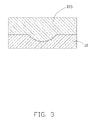
- a photoresist layer 105 is formed on the surface 101 and in the recess 103 .
- the photoresist layer 105 is formed by spin coating. In the spin coating process, the thickness of the photoresist layer 105 can be effectively controlled.
- a photomask 106 with a light transmissive part 108 is positioned over the photoresist layer 105 .
- the photoresist layer 105 is exposed by light (e.g., yellow light, ultraviolet light, etc) passing through the light transmissive part 108 , and is then developed using a developing solution (not shown). Thereby, a body of remaining photoresist 107 is retained in the recess 103 .
- the light transmissive part 108 is cylindrical or disk-shaped, such that the remaining photoresist 107 is correspondingly substantially cylindrical.
- the remaining photoresist 107 protrudes from the surface 101 , and the diameter of the remaining photoresist 107 is approximately 15 micrometers ( ⁇ m). In other embodiments, the remaining photoresist 107 may instead be shaped substantially as a triangular prism, a quadrangular prism, etc.
- a metal layer 109 is formed on the surface 101 and in unfilled areas of the recess 103 .
- the metal layer 109 substantially surrounds the remaining photoresist 107 .
- a top end portion of the remaining photoresist 107 protrudes out from a top of the metal layer 109 , and the metal layer 109 is made of copper.
- the top end portion of the remaining photoresist 107 may be flush with the top surface of the metal layer 109 .
- the metal layer 109 may instead be made of aluminum (Al), nickel, nickel-copper (Ni—Cu) alloy, etc.
- step S 5 referring to FIG. 7 , the remaining photoresist 107 is removed from the substrate 10 to form the alignment mark 20 surrounded by the metal layer 109 on the substrate 10 .
- This can be performed using, e.g., acetone organic solution.
- the alignment mark 20 is in the form of a cylindrical through hole in the metal layer 109 .
- the metal layer 109 is polished to make the top surface of the metal layer 109 substantially planar.
- the photoresist layer 105 is exposed and developed such that the remaining photoresist 107 has a relatively small size. Accordingly, the alignment mark 20 formed by removing the remaining photoresist 107 has a correspondingly small size.
Landscapes
- Engineering & Computer Science (AREA)
- Physics & Mathematics (AREA)
- General Physics & Mathematics (AREA)
- Chemical & Material Sciences (AREA)
- Nanotechnology (AREA)
- Crystallography & Structural Chemistry (AREA)
- Condensed Matter Physics & Semiconductors (AREA)
- Manufacturing & Machinery (AREA)
- Mathematical Physics (AREA)
- Theoretical Computer Science (AREA)
- Exposure And Positioning Against Photoresist Photosensitive Materials (AREA)
Abstract
An exemplary method for making an alignment mark on a substrate includes the following steps. First, a substrate with a recess is provided. Second, a photoresist layer is formed on a surface of the substrate including in the recess. Third, the photoresist layer is exposed and developed to leave a body of remaining photoresist in the recess, with the body of remaining photoresist protruding above the surface of the substrate. Fourth, a metal layer is formed in an unfilled area of the recess and on the surface of the substrate, with the metal layer substantially surrounding the remaining photoresist. Finally, the remaining photoresist is removed to form an alignment mark in the metal layer on the substrate.
Description
1. Technical Field
The present disclosure relates to a method for making an alignment mark on a substrate, such as a substrate that is subsequently used as a press mold.
2. Description of Related Art
With the ongoing development of optical imaging technology, wafer level lens modules are now widely used in electronic devices such as digital cameras, mobile phones, etc.
Generally, a wafer level lens module includes wafer level optical members, such as lenses, filters, etc, and a wafer level image sensor. In a process of manufacturing a wafer level lens module, a first wafer including many first wafer level optical members arranged in an array, a second wafer including many second wafer level optical members arranged in an array, and a third wafer including many wafer level image sensors arranged in an array are fabricated. Then in assembly, the first wafer is coupled to the second wafer, and subsequently is coupled to the third wafer to form a wafer level lens module array. Finally, the wafer level lens module array is cut into many individual wafer level lens modules by laser cutting. In the process of fabricating each of the first and second wafers, the first (second) wafer level optical members are formed by pressing a precision mold on a base material of the first (second) optical members arranged on a wafer. The precision mold includes a small substrate, which has many mold cavities arranged in an array therein.
When coupling the first wafer to the second wafer, the first wafer level optical members need to be precisely coaxial with the respective second wafer level optical members. Otherwise, so-called eccentricities occur. The eccentricities lower the quality of the wafer level lens modules. For assuring such coaxial alignment, at least one alignment mark is formed on the small substrate of the precision mold by a cutter. The alignment mark of the small substrate forms a corresponding alignment mark on each of the first and second wafers. Then when the first wafer is coupled to the second wafer, the alignment marks of the two wafers are aligned with each other. As a result, the first wafer level optical members can be coaxial with the respective second wafer level optical members.
However, because the edge of the cutter is rather thick, small alignment marks with narrower width cannot be formed on the small substrate of the precision mold.
Therefore, what is needed is a method for making an alignment mark on a substrate, which can overcome the limitations described above.
Many aspects of the present embodiments can be better understood with reference to the following drawings. The components in the drawings are not necessarily drawn to scale, the emphasis instead being placed upon clearly illustrating the principles of the present embodiments. Moreover, in the drawings, all the views are schematic, and like reference numerals designate corresponding parts throughout the several views.
Referring to FIGS. 1-2 , in step S1, the substrate 10 is firstly provided. In the present embodiment, the substrate 10 is made of nickel (Ni). In other embodiments, the substrate 10 may instead be made of silicon carbide (SiC), silicon nitride (Si3N4), platinum (Pt), aluminum oxide (Al2O3), etc. The substrate 10 includes a surface 101, and a recess 103 defined in the surface 101. In the present embodiment, the recess 101 is formed by a turning method.
In step S2, referring to FIG. 3 , a photoresist layer 105 is formed on the surface 101 and in the recess 103. In the present embodiment, the photoresist layer 105 is formed by spin coating. In the spin coating process, the thickness of the photoresist layer 105 can be effectively controlled.
In step S3, referring to FIGS. 4-5 , a photomask 106 with a light transmissive part 108 is positioned over the photoresist layer 105. The photoresist layer 105 is exposed by light (e.g., yellow light, ultraviolet light, etc) passing through the light transmissive part 108, and is then developed using a developing solution (not shown). Thereby, a body of remaining photoresist 107 is retained in the recess 103. In the present embodiment, the light transmissive part 108 is cylindrical or disk-shaped, such that the remaining photoresist 107 is correspondingly substantially cylindrical. The remaining photoresist 107 protrudes from the surface 101, and the diameter of the remaining photoresist 107 is approximately 15 micrometers (μm). In other embodiments, the remaining photoresist 107 may instead be shaped substantially as a triangular prism, a quadrangular prism, etc.
In step S4, referring to FIG. 6 , a metal layer 109 is formed on the surface 101 and in unfilled areas of the recess 103. The metal layer 109 substantially surrounds the remaining photoresist 107. In this embodiment, a top end portion of the remaining photoresist 107 protrudes out from a top of the metal layer 109, and the metal layer 109 is made of copper. In other embodiments, the top end portion of the remaining photoresist 107 may be flush with the top surface of the metal layer 109. The metal layer 109 may instead be made of aluminum (Al), nickel, nickel-copper (Ni—Cu) alloy, etc.
In step S5, referring to FIG. 7 , the remaining photoresist 107 is removed from the substrate 10 to form the alignment mark 20 surrounded by the metal layer 109 on the substrate 10. This can be performed using, e.g., acetone organic solution. In the present embodiment, because the remaining photoresist 107 is substantially cylindrical, the alignment mark 20 is in the form of a cylindrical through hole in the metal layer 109.
Referring also to FIG. 8 , the metal layer 109 is polished to make the top surface of the metal layer 109 substantially planar.
In the method for making the alignment mark 20 on the substrate 10, the photoresist layer 105 is exposed and developed such that the remaining photoresist 107 has a relatively small size. Accordingly, the alignment mark 20 formed by removing the remaining photoresist 107 has a correspondingly small size.
While certain embodiments have been described and exemplified above, various other embodiments will be apparent to those skilled in the art from the foregoing disclosure. The disclosure is not limited to the particular embodiments described and exemplified but is capable of considerable variation and modification without departure from the scope of the appended claims.
Claims (12)
1. A method for making an alignment mark on a substrate, the method comprising:
providing a substrate with a recess;
forming a photoresist layer on a surface of the substrate including in the recess;
exposing and developing the photoresist layer to leave a body of remaining photoresist in the recess, the remaining photoresist protruding above the surface of the substrate;
forming a metal layer in an unfilled area of the recess and on the surface of the substrate, the metal layer substantially surrounding the remaining photoresist; and
removing the remaining photoresist to form an alignment mark in the metal layer on the substrate.
2. The method of claim 1 , further comprising forming the recess in the substrate by a turning method.
3. The method of claim 1 , wherein after the metal layer is formed, the remaining photoresist protrudes from the metal layer.
4. The method of claim 1 , wherein the metal layer is comprised of material selected from the group consisting of copper, aluminum, nickel, and nickel-copper alloy.
5. The method of claim 1 , wherein the photoresist layer is formed by spin coating.
6. The method of claim 1 , wherein the alignment mark is in the form of a through hole in the metal layer.
7. The method of claim 6 , wherein the through hole has a shape selected from the group consisting of cylindrical and a polygonal prism.
8. A method for making an alignment mark on a substrate, the method comprising:
providing a substrate that has a surface;
forming a recess on the substrate by a turning method;
forming a photoresist layer on the surface of the substrate including in the recess by a spin coating method;
exposing and developing the photoresist layer to leave a portion of the photoresist remaining in the recess, the remaining portion of photoresist protruding above the surface of the substrate;
forming a metal layer on the surface of the substrate including an unfilled area of the recess, the metal layer substantially surrounding the portion of remaining photoresist; and
removing the portion of remaining photoresist to obtain an alignment mark in the metal layer on the substrate.
9. The method of claim 8 , wherein after the metal layer is formed, the portion of remaining photoresist protrudes from the metal layer.
10. The method of claim 8 , wherein the metal layer is comprised of material selected from the group consisting of copper, aluminum, nickel, and nickel-copper alloy.
11. The method of claim 8 , wherein the alignment mark is in the form of a through hole in the metal layer.
12. The method of claim 11 , wherein the through hole has a shape selected from the group consisting of cylindrical and a polygonal prism.
Applications Claiming Priority (3)
| Application Number | Priority Date | Filing Date | Title |
|---|---|---|---|
| CN200910301198.6 | 2009-03-30 | ||
| CN200910301198 | 2009-03-30 | ||
| CN2009103011986A CN101852985B (en) | 2009-03-30 | 2009-03-30 | Manufacturing method of substrate alignment mark |
Publications (2)
| Publication Number | Publication Date |
|---|---|
| US20100248161A1 US20100248161A1 (en) | 2010-09-30 |
| US8071276B2 true US8071276B2 (en) | 2011-12-06 |
Family
ID=42784705
Family Applications (1)
| Application Number | Title | Priority Date | Filing Date |
|---|---|---|---|
| US12/634,803 Expired - Fee Related US8071276B2 (en) | 2009-03-30 | 2009-12-10 | Method for making alignment mark on substrate |
Country Status (2)
| Country | Link |
|---|---|
| US (1) | US8071276B2 (en) |
| CN (1) | CN101852985B (en) |
Families Citing this family (2)
| Publication number | Priority date | Publication date | Assignee | Title |
|---|---|---|---|---|
| CN101875532B (en) * | 2009-04-30 | 2013-03-20 | 鸿富锦精密工业(深圳)有限公司 | Manufacturing method of lens mould |
| CN103426811B (en) * | 2012-05-15 | 2016-02-17 | 无锡华润上华科技有限公司 | Method, semi-conductor device manufacturing method and semiconductor device |
Citations (3)
| Publication number | Priority date | Publication date | Assignee | Title |
|---|---|---|---|---|
| US20020192926A1 (en) * | 2001-06-18 | 2002-12-19 | Schroeder Uwe Paul | High contrast lithography alignment marks for semiconductor manufacturing |
| US6979526B2 (en) * | 2002-06-03 | 2005-12-27 | Infineon Technologies Ag | Lithography alignment and overlay measurement marks formed by resist mask blocking for MRAMs |
| US20080305439A1 (en) * | 2007-06-07 | 2008-12-11 | Nitto Denko Corporation | Manufacturing method of optical waveguide |
Family Cites Families (9)
| Publication number | Priority date | Publication date | Assignee | Title |
|---|---|---|---|---|
| US4487653A (en) * | 1984-03-19 | 1984-12-11 | Advanced Micro Devices, Inc. | Process for forming and locating buried layers |
| JPH0475316A (en) | 1990-07-17 | 1992-03-10 | Fujitsu Ltd | Manufacture of semiconductor device |
| JP2976986B2 (en) | 1990-10-29 | 1999-11-10 | 富士通株式会社 | Method of forming alignment mark |
| JP2865089B2 (en) * | 1996-12-26 | 1999-03-08 | 日本電気株式会社 | Mark for measuring overlay accuracy and method for producing the same |
| JP3379478B2 (en) * | 1999-06-04 | 2003-02-24 | 日本電気株式会社 | Method for manufacturing semiconductor device |
| US6571485B1 (en) * | 2001-11-30 | 2003-06-03 | United Microelectronics Corp. | Structure of an overlay mark and its dosimetry application |
| DE102004014676B4 (en) * | 2004-03-25 | 2009-05-14 | Infineon Technologies Ag | Method for producing an integrated circuit arrangement with auxiliary recess, in particular with alignment marks, and integrated circuit arrangement |
| JP4735280B2 (en) * | 2006-01-18 | 2011-07-27 | 株式会社日立製作所 | Pattern formation method |
| JP2009015307A (en) * | 2007-06-07 | 2009-01-22 | Nitto Denko Corp | Manufacturing method of optical waveguide |
-
2009
- 2009-03-30 CN CN2009103011986A patent/CN101852985B/en not_active Expired - Fee Related
- 2009-12-10 US US12/634,803 patent/US8071276B2/en not_active Expired - Fee Related
Patent Citations (3)
| Publication number | Priority date | Publication date | Assignee | Title |
|---|---|---|---|---|
| US20020192926A1 (en) * | 2001-06-18 | 2002-12-19 | Schroeder Uwe Paul | High contrast lithography alignment marks for semiconductor manufacturing |
| US6979526B2 (en) * | 2002-06-03 | 2005-12-27 | Infineon Technologies Ag | Lithography alignment and overlay measurement marks formed by resist mask blocking for MRAMs |
| US20080305439A1 (en) * | 2007-06-07 | 2008-12-11 | Nitto Denko Corporation | Manufacturing method of optical waveguide |
Also Published As
| Publication number | Publication date |
|---|---|
| CN101852985A (en) | 2010-10-06 |
| US20100248161A1 (en) | 2010-09-30 |
| CN101852985B (en) | 2013-01-09 |
Similar Documents
| Publication | Publication Date | Title |
|---|---|---|
| JP4793618B2 (en) | CMOS image sensor structure and process for manufacturing a camera module using the same | |
| US8134118B2 (en) | Image capture unit and methods of fabricating a lens array block utilizing electrolysis | |
| TWI488499B (en) | Method, device and system for implementing lens calibration of light sensitive device | |
| TWI501864B (en) | Multilayer polymer lens and method of manufacturing same | |
| US9075182B2 (en) | Camera module and spacer of a lens structure in the camera module | |
| KR20060081202A (en) | Image sensor chip with protective plate and manufacturing method thereof | |
| US7796336B2 (en) | Lens, lens array and method for making lens array | |
| CN105870141A (en) | Curved image sensor systems and methods for manufacturing the same | |
| US8630042B2 (en) | Lens assembly and method for forming the same | |
| TW200525707A (en) | Semiconductor device and method of manufacturing the same | |
| US8071276B2 (en) | Method for making alignment mark on substrate | |
| KR101124652B1 (en) | Fabricating method of a wafer level module | |
| TWI313057B (en) | Manufacturing method of semiconductor device | |
| US20170213802A1 (en) | Semiconductor structure and manufacturing method thereof | |
| JP2012215655A (en) | Spacer manufacturing method and lens module manufacturing method | |
| US20080198481A1 (en) | Aspheric lens structures and fabrication methods thereof | |
| US6686214B2 (en) | Method of aligning a photolithographic mask to a crystal plane | |
| US20050087756A1 (en) | Light transmissive cover, device provided with same and methods for manufacturing them | |
| JPH081810A (en) | Microlens formed by isotropic etching | |
| KR100840765B1 (en) | Cantilever type probe manufacturing method | |
| KR100511890B1 (en) | method for fabricating semiconductor device | |
| TWI570873B (en) | Semiconductor structure and manufacturing method for the same | |
| CN103972250B (en) | The autoregistration that the wettability difference at interface produces | |
| CN114779572A (en) | Manufacturing method of alignment mark and wafer bonding method | |
| KR100937656B1 (en) | Semiconductor element and manufacturing method thereof |
Legal Events
| Date | Code | Title | Description |
|---|---|---|---|
| AS | Assignment |
Owner name: HON HAI PRECISION INDUSTRY CO., LTD., TAIWAN Free format text: ASSIGNMENT OF ASSIGNORS INTEREST;ASSIGNOR:LOUH, SEI-PING;REEL/FRAME:023633/0338 Effective date: 20091201 |
|
| REMI | Maintenance fee reminder mailed | ||
| LAPS | Lapse for failure to pay maintenance fees | ||
| STCH | Information on status: patent discontinuation |
Free format text: PATENT EXPIRED DUE TO NONPAYMENT OF MAINTENANCE FEES UNDER 37 CFR 1.362 |
|
| STCH | Information on status: patent discontinuation |
Free format text: PATENT EXPIRED DUE TO NONPAYMENT OF MAINTENANCE FEES UNDER 37 CFR 1.362 |
|
| FP | Lapsed due to failure to pay maintenance fee |
Effective date: 20151206 |