US8064490B2 - Optical resonator and tunable laser - Google Patents
Optical resonator and tunable laser Download PDFInfo
- Publication number
- US8064490B2 US8064490B2 US12/458,686 US45868609A US8064490B2 US 8064490 B2 US8064490 B2 US 8064490B2 US 45868609 A US45868609 A US 45868609A US 8064490 B2 US8064490 B2 US 8064490B2
- Authority
- US
- United States
- Prior art keywords
- optical
- mach
- optical waveguide
- waveguide
- resonator
- Prior art date
- Legal status (The legal status is an assumption and is not a legal conclusion. Google has not performed a legal analysis and makes no representation as to the accuracy of the status listed.)
- Active
Links
- 230000003287 optical effect Effects 0.000 title claims abstract description 266
- VYPSYNLAJGMNEJ-UHFFFAOYSA-N Silicium dioxide Chemical compound O=[Si]=O VYPSYNLAJGMNEJ-UHFFFAOYSA-N 0.000 claims description 30
- 239000004065 semiconductor Substances 0.000 claims description 23
- 239000000377 silicon dioxide Substances 0.000 claims description 15
- 230000008878 coupling Effects 0.000 claims description 13
- 238000010168 coupling process Methods 0.000 claims description 13
- 238000005859 coupling reaction Methods 0.000 claims description 13
- 235000012239 silicon dioxide Nutrition 0.000 claims description 13
- 238000005253 cladding Methods 0.000 claims description 12
- 239000000758 substrate Substances 0.000 claims description 11
- 229910052710 silicon Inorganic materials 0.000 claims description 9
- 239000010703 silicon Substances 0.000 claims description 9
- 239000000463 material Substances 0.000 claims description 6
- 239000011248 coating agent Substances 0.000 claims description 3
- 238000000576 coating method Methods 0.000 claims description 3
- 150000001875 compounds Chemical class 0.000 claims description 2
- 230000001629 suppression Effects 0.000 description 11
- 230000003595 spectral effect Effects 0.000 description 9
- XUIMIQQOPSSXEZ-UHFFFAOYSA-N Silicon Chemical group [Si] XUIMIQQOPSSXEZ-UHFFFAOYSA-N 0.000 description 7
- 230000007246 mechanism Effects 0.000 description 6
- 230000000694 effects Effects 0.000 description 4
- 230000002269 spontaneous effect Effects 0.000 description 4
- 230000008859 change Effects 0.000 description 3
- 238000004891 communication Methods 0.000 description 3
- 229910052581 Si3N4 Inorganic materials 0.000 description 2
- 238000013459 approach Methods 0.000 description 2
- 230000003247 decreasing effect Effects 0.000 description 2
- 230000001066 destructive effect Effects 0.000 description 2
- 238000000034 method Methods 0.000 description 2
- 230000008569 process Effects 0.000 description 2
- 230000001902 propagating effect Effects 0.000 description 2
- HQVNEWCFYHHQES-UHFFFAOYSA-N silicon nitride Chemical compound N12[Si]34N5[Si]62N3[Si]51N64 HQVNEWCFYHHQES-UHFFFAOYSA-N 0.000 description 2
- 229910000530 Gallium indium arsenide Inorganic materials 0.000 description 1
- KXNLCSXBJCPWGL-UHFFFAOYSA-N [Ga].[As].[In] Chemical group [Ga].[As].[In] KXNLCSXBJCPWGL-UHFFFAOYSA-N 0.000 description 1
- 230000003321 amplification Effects 0.000 description 1
- 230000005540 biological transmission Effects 0.000 description 1
- 230000006872 improvement Effects 0.000 description 1
- 238000003199 nucleic acid amplification method Methods 0.000 description 1
- 239000013307 optical fiber Substances 0.000 description 1
- 230000000737 periodic effect Effects 0.000 description 1
- 230000000644 propagated effect Effects 0.000 description 1
- 230000006798 recombination Effects 0.000 description 1
- 238000005215 recombination Methods 0.000 description 1
- 238000002310 reflectometry Methods 0.000 description 1
Images


Classifications
-
- G—PHYSICS
- G02—OPTICS
- G02B—OPTICAL ELEMENTS, SYSTEMS OR APPARATUS
- G02B6/00—Light guides; Structural details of arrangements comprising light guides and other optical elements, e.g. couplings
- G02B6/24—Coupling light guides
- G02B6/26—Optical coupling means
- G02B6/28—Optical coupling means having data bus means, i.e. plural waveguides interconnected and providing an inherently bidirectional system by mixing and splitting signals
- G02B6/293—Optical coupling means having data bus means, i.e. plural waveguides interconnected and providing an inherently bidirectional system by mixing and splitting signals with wavelength selective means
- G02B6/29346—Optical coupling means having data bus means, i.e. plural waveguides interconnected and providing an inherently bidirectional system by mixing and splitting signals with wavelength selective means operating by wave or beam interference
- G02B6/2935—Mach-Zehnder configuration, i.e. comprising separate splitting and combining means
- G02B6/29352—Mach-Zehnder configuration, i.e. comprising separate splitting and combining means in a light guide
- G02B6/29355—Cascade arrangement of interferometers
-
- H—ELECTRICITY
- H01—ELECTRIC ELEMENTS
- H01S—DEVICES USING THE PROCESS OF LIGHT AMPLIFICATION BY STIMULATED EMISSION OF RADIATION [LASER] TO AMPLIFY OR GENERATE LIGHT; DEVICES USING STIMULATED EMISSION OF ELECTROMAGNETIC RADIATION IN WAVE RANGES OTHER THAN OPTICAL
- H01S5/00—Semiconductor lasers
- H01S5/02—Structural details or components not essential to laser action
- H01S5/026—Monolithically integrated components, e.g. waveguides, monitoring photo-detectors, drivers
- H01S5/0265—Intensity modulators
-
- H—ELECTRICITY
- H01—ELECTRIC ELEMENTS
- H01S—DEVICES USING THE PROCESS OF LIGHT AMPLIFICATION BY STIMULATED EMISSION OF RADIATION [LASER] TO AMPLIFY OR GENERATE LIGHT; DEVICES USING STIMULATED EMISSION OF ELECTROMAGNETIC RADIATION IN WAVE RANGES OTHER THAN OPTICAL
- H01S5/00—Semiconductor lasers
- H01S5/10—Construction or shape of the optical resonator, e.g. extended or external cavity, coupled cavities, bent-guide, varying width, thickness or composition of the active region
- H01S5/1003—Waveguide having a modified shape along the axis, e.g. branched, curved, tapered, voids
-
- H—ELECTRICITY
- H01—ELECTRIC ELEMENTS
- H01S—DEVICES USING THE PROCESS OF LIGHT AMPLIFICATION BY STIMULATED EMISSION OF RADIATION [LASER] TO AMPLIFY OR GENERATE LIGHT; DEVICES USING STIMULATED EMISSION OF ELECTROMAGNETIC RADIATION IN WAVE RANGES OTHER THAN OPTICAL
- H01S5/00—Semiconductor lasers
- H01S5/50—Amplifier structures not provided for in groups H01S5/02 - H01S5/30
Definitions
- the present invention relates to an optical resonator and a tunable laser.
- Tunable lasers are widely used to generate light of different wavelengths in wavelength division multiplexed communication systems, because they enable a single device to handle a plurality of wavelengths.
- Numerous tunable laser structures have been proposed, as disclosed in, for example, Japanese Patent Application Publications No. H10-261837, 2000-261086, 2000-223744, 2005-327881, 2002-6352, 2004-71809, 2006-196554, 2007-115900, and 2007-234786, and by Takahashi et al. in ‘Tunable Lasers Based on Silica Waveguide Ring Resonators’, Optical Fiber Communication Conference Papers 2008, OWJ1.
- a common feature of the tunable lasers in these disclosures is that they include a semiconductor optical amplifier and a tunable filter in an optical resonator.
- the tunable laser disclosed by Takahashi et al. uses two ring resonators with different free spectral ranges, and enables the wavelength to be tuned by the Vernier effect of the wavelength transmission peak.
- a ring resonator for supplying a reference wavelength is also included; used together with the Vernier effect, it enables the wavelength band of the selected light to be varied over a comparatively wide range of fifty nanometers (50 nm) with only a slight change in refractive index.
- This tunable laser is made from materials with a high refractive index, so the radius of curvature of the optical waveguide can be small enough to reduce the laser device to a square measuring about five millimeters (5 mm) on each side.
- the resonant wavelengths of the two ring resonators in the tunable laser disclosed by Takahashi et al. must, however, be precisely controlled, requiring a complex control circuit. There is moreover a need for an optical resonator even smaller than the optical resonators in the tunable laser disclosed by Takahashi et al.
- An object of the present invention is to provide a simpler way to control wavelength through use of a single parameter, more specifically through the use of a refractive index parameter.
- Another object of the invention is to provide an optical resonator and tunable laser with reduced size.
- a novel optical resonator having first, second, and third optical waveguides with ends interconnected at a single point to form a Y-branch.
- the first waveguide is terminated at its other end by a reflector.
- One or both of the second and third waveguides includes a wavelength selector.
- the second and third waveguides are optically coupled by an optical connecting path disposed between their other (terminal) ends.
- the optical connecting path may be a curved optical waveguide that interconnects the terminal ends of the second and third waveguides, so that the curved optical waveguide and the second and third optical waveguides form a loop optical waveguide.
- the optical connecting path may itself be a loop optical waveguide, to which the terminal ends of the second and third waveguides are optically coupled.
- These optical couplings may be directional couplings formed by a first part of the loop optical waveguide that passes adjacent to the terminal end of the second optical waveguide, and a second part of the loop optical waveguide that passes adjacent to the terminal end of the second optical waveguide.
- the wavelength selector may be a Mach-Zehnder interferometer.
- the first n- 1 Mach-Zehnder interferometers may be placed on the second optical waveguide and the n-th Mach-Zehnder interferometer may be placed on the third optical waveguide.
- a novel tunable laser is made by inserting an optical amplifier between the terminal end of the first optical waveguide and the reflector, which may be a reflective coating on the optical amplifier.
- novel optical resonator and tunable laser can be made smaller than was possible in the prior art, and permits the resonant or lasing wavelength to be controlled by refractive index alone.
- FIG. 1 is a schematic perspective view of an optical resonator in a first embodiment of the invention
- FIG. 2 is an enlarged plan view of point P in FIG. 1 ;
- FIG. 3 is an enlarged plan view of the first Mach-Zehnder interferometer in FIG. 1 ;
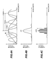
- FIG. 4A is a graph schematically depicting the wavelength selection characteristics of the three Mach-Zehnder interferometers in FIG. 1 ;
- FIG. 4B is a graph schematically depicting the combined wavelength selection characteristic of the three Mach-Zehnder interferometers in FIG. 1 ;
- FIG. 4C is a schematic redrawing of FIG. 4B , also indicating the Fabry-Perot resonant wavelengths.
- FIG. 5 is a graph illustrating side mode suppression characteristics in several versions of the first embodiment
- FIG. 6 is a schematic perspective view of an optical resonator in a variation of the first embodiment of the invention.
- FIG. 7 is a schematic perspective view of an optical resonator in a second embodiment of the invention.
- FIG. 8A is a graph schematically depicting the combined wavelength selection characteristic of the three Mach-Zehnder interferometers in FIG. 7 ;
- FIG. 8B is a graph schematically depicting the wavelength selection characteristic of the loop optical waveguide in FIG. 7 ;
- FIG. 8C is a graph schematically depicting the combined wavelength selection characteristic of the three Mach-Zehnder interferometers and the loop optical waveguide in FIG. 7 ;
- FIG. 9 is a graph illustrating side mode suppression characteristics in several versions of the second embodiment.
- the first embodiment provides an optical resonator and a tunable laser with the structure illustrated in FIGS. 1 to 3 .
- the optical resonator 10 includes three optical waveguides 12 , 14 , 16 that meet at a point P to form a Y-branched waveguide 18 .
- the second optical waveguide 14 includes first and second Mach-Zehnder interferometers 19 and 20 .
- the third optical waveguide 16 includes a third Mach-Zehnder interferometer 21 .
- the terminal ends 14 a and 14 b of the second and third optical waveguides 12 and 14 (the ends distant from point P) are joined by a curved optical waveguide 22 .
- the optical resonator 10 also includes a reflector 24 and a semiconductor optical amplifier 26 disposed between the reflector 24 and the first optical waveguide 12 .
- the optical resonator 10 is formed as an integrated device on a major surface 28 a of a substrate 28 .
- the reflector 24 and semiconductor optical amplifier 26 are formed directly on the major surface 28 a .
- the Y-branched waveguide 18 including the Mach-Zehnder interferometers 19 , 20 , 21 , and the curved optical waveguide 22 are embedded in a silicon dioxide film 30 deposited on the major surface 28 a .
- the Y-branched waveguide 18 and curved optical waveguide 22 are indicated by solid lines even though they are interior to the silicon dioxide film 30 and are not exposed on the surface of the silicon dioxide film 30 .
- FIG. 1 is just one example of a more general configuration in which there are n Mach-Zehnder interferometers, where n may be any integer greater than unity.
- the Mach-Zehnder interferometers may be divided between the second and third optical waveguides 14 , 16 in any way, or all of the Mach-Zehnder interferometers may be placed on just one of the second and third optical waveguides.
- the substrate 28 is preferably a flat rectangular substrate.
- One preferred material from which the substrate 28 may be made is silicon.
- the reflector 24 is a known dielectric multilayer film with a reflectivity of at least 90% but less than 100%.
- One preferred type of reflector 24 comprises alternating layers of silicon nitride (SiN) and silicon dioxide (SiO 2 ).
- the reflector 24 is formed as a coating on the end of the semiconductor optical amplifier 26 from which light is to be output from the optical resonator 10 .
- the semiconductor optical amplifier 26 is a known semiconductor laser light source comprising a light-emitting active layer sandwiched between a p-type clad layer and an n-type clad layer (these layers are not shown). Some or all of these layers may be made from compound semiconductor materials.
- One preferred material from which the active layer may be made is indium gallium arsenide phosphide (InGaAsP), which emits light with a wavelength of 1.55 ⁇ m. Light is emitted when current is supplied to the semiconductor optical amplifier 26 through electrodes (not shown).
- the semiconductor optical amplifier 26 emits light from both ends. At one end, light is emitted through the reflector 24 . Light emitted from the other end of the semiconductor optical amplifier 26 is coupled into the first optical waveguide 12 .
- the silicon dioxide film 30 deposited on the major surface 28 a of the substrate 28 has a flat rectangular shape and a size smaller than the size of the substrate 28 .
- the silicon dioxide film 30 functions as a cladding with respect to the embedded Y-branched waveguide 18 , including the Mach-Zehnder interferometers 19 , 20 , 21 , and the embedded curved optical waveguide 22 .
- the optical waveguides 12 , 14 , 16 embedded in the silicon dioxide cladding film 30 that form the Y-branched waveguide 18 are preferably silicon waveguides.
- Each of these waveguides preferably has a square cross sectional shape with height and width dimensions of, for example, 0.3 ⁇ m.
- the height dimension is orthogonal to the major surface 28 a of the substrate 28 and orthogonal to the direction of light propagation in the waveguide.
- the width dimension is parallel to the major surface 28 a of the substrate 28 and orthogonal to the direction of light propagation.
- the first optical waveguide 12 extends in a straight line from its initial end at point P to its terminal end 12 a, which faces the active layer of the semiconductor optical amplifier 26 .
- the terminal end 12 a of the first optical waveguide 12 is preferably disposed so that its optical field distribution matches the optical field distribution of the active layer in the semiconductor optical amplifier 26 .
- the terminal end 12 a of the first optical waveguide 12 may be separated from the active layer by a suitable distance, such as a few micrometers, provided this distance is small enough to permit optical coupling.
- the second and third optical waveguides 14 and 16 branch symmetrically from point P.
- the branching angle is exaggerated for clarity in the drawings.
- the central axes of the three waveguides form angles ⁇ , ⁇ , ⁇ as shown in FIG. 2 .
- the angle ⁇ between the longitudinal axes of the second and third waveguides 14 and 16 is preferably about 0.5 degrees.
- the angles ⁇ , ⁇ between the longitudinal axes of the second and third waveguides 14 and 16 and the longitudinal axis of the first optical waveguide 12 is preferably about 0.25 degrees. With these angles, all of the light propagating through the second optical waveguide 14 (or the third optical waveguide 16 ) toward point P propagates into the first optical waveguide 12 and is not diverted into the third optical waveguide 16 (or second optical waveguide 14 ).
- the second and third optical waveguides 14 and 16 are mutually symmetric with respect to a line C forming an extension of the axis of the first optical waveguide 12 .
- the second and third optical waveguides 14 and 16 accordingly have the same optical path length.
- the second and third optical waveguides 14 and 16 both branch away from point P in an S-pattern, then extend straight, parallel to line C, out to their terminal ends 14 a , 16 a .
- the Mach-Zehnder interferometers 19 , 20 , 21 are formed in the straight segments.
- the terminal ends 14 a , 16 a of the second and third optical waveguides 14 and 16 are optically coupled to the curved optical waveguide 22 so that the second and third optical waveguides 14 and 16 and the curved optical waveguide 22 form a first loop optical waveguide 32 .
- the curved optical waveguide 22 is a silicon waveguide similar to the second and third optical waveguides 14 and 16 and has the same cross sectional dimensions. In the present embodiment the curved optical waveguide 22 is integral with the second and third optical waveguides 14 and 16 , forming a curved continuation of the second and third optical waveguides 14 and 16 .
- the curved optical waveguide 22 has, for example, a semicircular shape.
- the radius of curvature of the curved optical waveguide 22 should be large enough to hold the loss of light propagating in the curved optical waveguide 22 to an acceptable level.
- the radius of curvature of the curved optical waveguide 22 may be, for example, about 0.3 mm.
- the first Mach-Zehnder interferometer 19 comprises a pair of Y-branches 19 a , 19 b joined by two straight arms 19 c , 19 d .
- An electrode 19 e is provided on arm 19 c.
- the two arms 19 c , 19 d have different optical path lengths L 19 c and L 19 d .
- the arm 19 c with the electrode 19 e has the shorter optical path length (L 19 c ⁇ L 19 d ).
- the difference (L 19 d -L 19 c ) between the two optical path lengths will be denoted ⁇ L 1 .
- the length of the electrode 19 e on arm 19 c will be denoted Le 1 .
- the refractive index of arm 19 c changes due to thermo-optic and electro-optic effects.
- the optical path length of arm 19 c is thereby controlled by the voltage applied to the electrode 19 e; this feature is used for wavelength tuning.
- first Mach-Zehnder interferometer 19 Light entering the first Mach-Zehnder interferometer 19 at Y-branch 19 a propagates through both arms 19 c , 19 d .
- a phase difference arises due to the difference ⁇ L 1 in the optical path length of the two arms 19 c , 19 d .
- the recombining light may interfere constructively or destructively, depending on its wavelength and the value of ⁇ L 1 . This enables the first Mach-Zehnder interferometer 19 to operate as a means of wavelength selection.
- the second and third Mach-Zehnder interferometers 20 , 21 are similar to the first Mach-Zehnder interferometer 19 , but have different lengths.
- the optical path length differences between their arms will be denoted ⁇ L 2 and ⁇ L 3 , respectively.
- the lengths of their electrodes will be denoted Le 2 and Le 3 , respectively.
- ⁇ L 1 ⁇ L 1 ⁇ 2 i-1
- Lei Le 1 ⁇ 2 i-1
- Light generated in the semiconductor optical amplifier 26 propagates through the first optical waveguide 12 to the branching point P of the Y-branched waveguide 18 , and is divided equally between the second optical waveguide 14 and third optical waveguide 16 .
- the light that enters the second optical waveguide 14 undergoes wavelength selection in the first and second Mach-Zehnder interferometers 19 , 20 .
- the wavelength selection mechanism will be described in more detail later.
- Light of wavelengths rejected by these Mach-Zehnder interferometers 19 , 20 is dissipated in the silicon dioxide cladding film 30 .
- the light that passes through the first and second Mach-Zehnder interferometers 19 , 20 proceeds through the curved optical waveguide 22 , which changes its direction of travel by 180 degrees, and enters the third optical waveguide 16 .
- the Mach-Zehnder interferometer 21 in the third optical waveguide 16 performs a further wavelength selection process.
- light that enters the third optical waveguide 16 from point P undergoes wavelength selection in the third Mach-Zehnder interferometer 21 , then travels around the curved optical waveguide 22 , enters the second optical waveguide 14 , and undergoes further wavelength selection in the first and second Mach-Zehnder interferometers 19 , 20 .
- the light emitted in the semiconductor optical amplifier 26 that reaches point P through the first optical waveguide 12 is divided into two equal parts that travel around the first loop optical waveguide 32 in the clockwise direction (third optical waveguide 16 to curved optical waveguide 22 to second optical waveguide 14 ) and counterclockwise direction (second optical waveguide 14 to curved optical waveguide 22 to third optical waveguide 16 ), respectively, then recombine at point P. Since both parts of the light traverse the same optical path, albeit in opposite directions, when they return to point P they are mutually in phase and recombine constructively; no light is lost by destructive interference.
- the recombined light propagates through the first optical waveguide 12 and semiconductor optical amplifier 26 to the reflector 24 , where most of the light is reflected back through the semiconductor optical amplifier 26 to repeat the process described above, again and again.
- the light is amplified in each repetition.
- amplification in the semiconductor optical amplifier 26 is balanced by loss in the waveguides and by escape of some of the light through the reflector 24 .
- the escaping light is emitted as a laser beam, indicated by the arrow at the left in FIG. 1 .
- the wavelength selection mechanism will now be described in more detail with reference to the graphs in FIGS. 4A to 4C .
- the horizontal axis represents wavelength and the vertical axis represents light intensity, both in arbitrary units.
- FIG. 4A schematically illustrates the wavelength selectivity characteristics of the three Mach-Zehnder interferometers 19 , 20 , 21 .
- Curve I represents the wavelength selectivity of the first Mach-Zehnder interferometer 19 when white light including all wavelengths enters at Y-branch 19 a and exits at Y-branch 19 b .
- curve II represents the wavelength selectivity of the second Mach-Zehnder interferometer 20 when white light including all wavelengths enters at Y-branch 20 a and exits at Y-branch 20 b
- curve III represents the wavelength selectivity of the third Mach-Zehnder interferometer 21 when white light including all wavelengths enters at Y-branch 21 a and exits at Y-branch 21 b.
- All three selectivity curves I, II, III are periodic. Their peak-to-peak distances, referred to as their free spectral ranges, decrease with increasing arm length. Thus the free spectral range FRS19 of the first Mach-Zehnder interferometer 19 is greater than the free spectral range FRS20 of the second Mach-Zehnder interferometer 20 , which is in turn greater than the free spectral range FRS21 of the third Mach-Zehnder interferometer 21 .
- the three wavelength selectivity curves I, II, III in FIG. 4A have a common peak at a wavelength denoted ⁇ S in FIG. 4B .
- FIG. 4B schematically shows the combined wavelength selectivity curve of the three Mach-Zehnder interferometers 19 , 20 , 21 , obtained by multiplying the three curves I, II, III together.
- the multiple peaks of varying widths in FIG. 4A are reduced to substantially a single comparatively narrow peak in FIG. 4B .
- the optical resonator 10 also operates as a type of Fabry-Perot resonator between the reflector 24 and the first loop optical waveguide 32 , so the wavelengths of the light actually output from the optical resonator 10 are restricted to the longitudinal modes permitted by the Fabry-Perot resonator structure. These modes are indicated by vertical bars in FIG. 4C . The bar height is limited by the combined selectivity curve in FIG. 4B , indicated as a dotted line in FIG. 4C .
- the wavelength ⁇ SS that experiences the least loss in the optical resonator 10 represents the permitted longitudinal mode closest to the peak wavelength ⁇ S in FIG. 4B ; light of this wavelength is emitted most strongly from the optical resonator 10 . Additional side modes, represented by lower vertical bars in FIG. 4C , also generate some light emission.
- the sharpness of the wavelength selectivity of the optical resonator 10 can be represented by the side mode suppression ratio R, which is the ratio of the emitted power of the light with wavelength ⁇ SS to the emitted power of the nearest side mode ⁇ ′.
- the side mode suppression ratio R (shown in decibels on the vertical axis) depends on the current density J in the semiconductor optical amplifier 26 .
- the horizontal axis in FIG. 5 represents the current density J normalized with respect to the threshold current J th at which light emission begins, so that the value of J/J th on the horizontal axis is dimensionless.
- the side mode suppression ratio R also depends on the number n of Mach-Zehnder interferometers in the optical resonator 10 , and the spontaneous emission coupling coefficient Cs of the semiconductor optical amplifier 26 , which is determined by the structure and composition of the semiconductor optical amplifier 26 .
- curves I-IV are shown, representing different combinations of n (4 or 5) and Cs (10 ⁇ 4 or 10 ⁇ 5 ). These curves were derived under the assumption that the length of the semiconductor optical amplifier 26 in the direction of light propagation was 0.3 mm.
- a side mode suppression ratio R of at least thirty decibels (30 dB) is generally held to be desirable. As indicated by curve IV in FIG. 5 , this value is attained or exceeded, over virtually the entire normalized current density (J/J th ) range from two to four, when the spontaneous emission coupling coefficient Cs is 10 ⁇ 5 and there are five Mach-Zehnder interferometers.
- the ratio Le/ ⁇ L is the same for all the Mach-Zehnder interferometers in the present embodiment, if all of the Mach-Zehnder interferometers have the same refractive index ns, their individual wavelength selectivity curves can be shifted by the same amount ⁇ by changing their refractive indexes by the same amount ⁇ ns. That is, the optical resonator 10 can be tuned by controlling a single refractive index parameter.
- Exemplary dimensions for the optical resonator 10 can be calculated as follows.
- the free spectral range must be at least 50 nm. If the Mach-Zehnder interferometers 19 , 20 , 21 are assumed to be silicon structures with a refractive index of about three (ns ⁇ 3), and if the wavelength ⁇ is assumed to be 1.55 ⁇ m, a wavelength which is often used in optical communications, then equation (1) shows that the optical path length difference should be at least about 8 ⁇ m.
- equation (2) indicates an electrode length of about 80 ⁇ m, and the first loop optical waveguide 32 can be reduced to a dimension of about 1.5 mm.
- the change ⁇ ns in the refractive index is obtained by varying the voltage applied to the electrodes 19 e , 20 e , 21 e of the Mach-Zehnder interferometers 19 , 20 , 21 .
- the wavelength at which the optical resonator 10 operates can be controlled by varying a single voltage.
- the length of the longest Mach-Zehnder interferometer is approximately equal to the sum of the lengths of the other Mach-Zehnder interferometers. If the longest Mach-Zehnder interferometer is placed in the third optical waveguide 16 and the other Mach-Zehnder interferometers are placed in the second optical waveguide 14 as in FIG. 1 , then the necessary length of the second and third optical waveguides 14 , 16 is only the length necessary to accommodate the longest Mach-Zehnder interferometer.
- the total length of the optical resonator 10 is accordingly only about half the length that would be necessary if all of the Mach-Zehnder interferometers were to be placed in a single linear waveguide, and the dimensions of the optical resonator 10 can be much smaller than the dimensions of the tunable laser described by Takahashi et al.
- the Y-branches 19 a , 19 b , 20 a , 20 b , 21 a , 21 b of the Mach-Zehnder interferometers in FIG. 1 are replaced by two-by-two optical couplers 34 a , 34 b , 36 a , 36 b , 38 a , 38 b as shown in FIG. 6 .
- Multi-mode interference couplers or directional couplers may be used. This variation permits one of the arms in each Mach-Zehnder interferometer to be extended beyond one of the couplers.
- the extended arm waveguides function as optical exit waveguides 34 c , 36 c , 38 c that lead unwanted light to the exterior of the optical resonator device.
- the light led out through the optical exit waveguides 34 c , 36 c , 38 c can be monitored to verify the wavelengths selected by the Mach-Zehnder interferometers.
- the second embodiment replaces the curved optical waveguide that joined the terminal ends 14 a , 16 a of the second and third optical waveguides 14 , 16 in the first embodiment with a second loop optical waveguide 42 .
- the optical resonator 40 in FIG. 7 is identical to the optical resonator in the first embodiment.
- the second loop optical waveguide 42 is not physically joined to the terminal ends 14 a , 16 a of the second and third optical waveguides 14 , 16 , the second loop optical waveguide 42 approaches the terminal ends 14 a , 16 a of the second and third optical waveguides 14 , 16 closely enough for an optical coupling to be obtained.
- the regions of close approach between the second loop optical waveguide 42 and the terminal ends 14 a , 16 a of the second and third optical waveguides 14 , 16 form a pair of directional couplers 44 , 46 .
- the second loop optical waveguide 42 itself forms a non-terminated substantially circular optical ring resonator embedded in the silicon dioxide cladding film 30 between the terminal ends 14 a , 16 a of the second and third optical waveguides 14 , 16 .
- the second loop optical waveguide 42 is preferably a silicon waveguide with the same cross-sectional dimensions as the second and third optical waveguides 14 , 16 .
- the radius of curvature of the second loop optical waveguide 42 may be selected according to the operating wavelength range of the optical resonator 40 ; one preferred value for the radius of curvature is approximately 0.3 mm.
- light emitted in the semiconductor optical amplifier 26 toward the first optical waveguide 12 is divided at point P into two equal parts.
- the part that propagates through the second optical waveguide 14 undergoes wavelength selection by the first and second Mach-Zehnder interferometers 19 , 20 .
- Light of the selected wavelengths is coupled into the second loop optical waveguide 42 by directional coupler 44 and begins circulating around the second loop optical waveguide 42 .
- the light interferes with further light entering the second loop optical waveguide 42 from the 14 a of the second optical waveguide 14 .
- the interference may be constructive or destructive.
- Light of wavelengths that satisfy the resonance condition of the second loop optical waveguide 42 interferes constructively and increases in intensity as it circulates repeatedly around the second loop optical waveguide 42 .
- Light of other wavelengths is dissipated into the silicon dioxide cladding film 30 .
- a fraction is coupled by directional coupler 46 into the third optical waveguide 16 and propagates back to point P, undergoing further wavelength selection in the third Mach-Zehnder interferometer 21 .
- this light recombines with light that has propagated in the opposite direction, from the third optical waveguide 16 through directional coupler 46 into the second loop optical waveguide 42 , then from the second loop optical waveguide 42 through directional coupler 44 into the second optical waveguide 14 and back to point P.
- the recombination is constructive because both parts of the light have traveled over the same path length in the second and third optical waveguides 14 , 16 and because both parts satisfy the condition for resonance in the second loop optical waveguide 42 .
- the wavelength selection mechanism in the second embodiment is illustrated by the graphs in FIGS. 8A , 8 B, and 8 C, which indicate wavelength on the horizontal axis and optical intensity on the vertical axis, both in arbitrary units.
- the wavelength selection mechanism in the second embodiment differs from the wavelength selection mechanism in the first embodiment in that the second loop optical waveguide 42 is also involved.
- FIG. 8A (identical to FIG. 4B ) illustrates the combined wavelength selectivity characteristic of the three Mach-Zehnder interferometers 19 , 20 , 21 .
- FIG. 8B illustrates the wavelength selectivity characteristic of the second loop optical waveguide 42 .
- the equally spaced peaks represent wavelengths that satisfy the resonance condition in the second loop optical waveguide 42 .
- the dotted line in FIG. 8C represents the combination of the wavelength selectivity characteristics in FIGS. 8A and 8B .
- the vertical bars in FIG. 8C represent the permitted longitudinal modes of the optical resonator 40 and indicate the degrees to which they are selected.
- FIG. 8C A comparison of FIG. 8C with FIG. 4C shows that the second embodiment has a much higher side mode suppression ratio than the second embodiment.
- the side mode suppression ratio R in the second embodiment is shown in FIG. 9 for the same combinations of the number n of Mach-Zehnder interferometers and the spontaneous emission coupling coefficient Cs and normalized current density values J/J th as in the first embodiment.
- FIG. 5 Compared with the first embodiment ( FIG. 5 ), there is an improvement of ten to fifteen decibels for all combinations of n, Cs, and J/J th .
- the second embodiment provides substantially the same effect as the first embodiment, but the second embodiment offers considerably better wavelength selectivity.
- the light output from the optical resonator 40 in the second embodiment is limited to wavelengths that satisfy the resonance condition of the second loop optical waveguide 42 .
- Mach-Zehnder interferometers are used for wavelength selection in the second and third optical waveguides 14 , 16 , but the use of other types of tunable wavelength selectors is also contemplated.
- optical resonators in the preceding embodiments operate as lasers, but the optical amplifier 26 may be removed if only operation as a resonator is required.
- the reflector 24 may be replaced by a reflector directly facing the terminal end 12 a of the first optical waveguide 12 .
Landscapes
- Physics & Mathematics (AREA)
- General Physics & Mathematics (AREA)
- Optics & Photonics (AREA)
- Condensed Matter Physics & Semiconductors (AREA)
- Electromagnetism (AREA)
- Optical Integrated Circuits (AREA)
- Lasers (AREA)
- Semiconductor Lasers (AREA)
- Optical Modulation, Optical Deflection, Nonlinear Optics, Optical Demodulation, Optical Logic Elements (AREA)
Abstract
Description
ΔLi=ΔL1×2i-1
Lei=Le1×2i-1
ΔL1=ΔL1×2i-1
Lei=Le1×2i-1
FSR=λ 2/(2nsΔL) (1)
where ns is the refractive index of the material of the Mach-Zehnder interferometer, ΔL is the optical path length difference between the two arms, and λ is the wavelength of the light. For a given refractive index and wavelength, a doubling of the path length difference ΔL reduces the free spectral range by a factor of two. Since the three Mach-
Δλ=λΔnsLe/(−nsΔL) (2)
Claims (12)
ΔLi=ΔL1×2i−1
Lei=Le1×2i−1,
Applications Claiming Priority (2)
| Application Number | Priority Date | Filing Date | Title |
|---|---|---|---|
| JP2008260896A JP5304158B2 (en) | 2008-10-07 | 2008-10-07 | Optical resonator and tunable laser |
| JP2008-260896 | 2008-10-07 |
Publications (2)
| Publication Number | Publication Date |
|---|---|
| US20100085991A1 US20100085991A1 (en) | 2010-04-08 |
| US8064490B2 true US8064490B2 (en) | 2011-11-22 |
Family
ID=42075774
Family Applications (1)
| Application Number | Title | Priority Date | Filing Date |
|---|---|---|---|
| US12/458,686 Active US8064490B2 (en) | 2008-10-07 | 2009-07-20 | Optical resonator and tunable laser |
Country Status (2)
| Country | Link |
|---|---|
| US (1) | US8064490B2 (en) |
| JP (1) | JP5304158B2 (en) |
Cited By (5)
| Publication number | Priority date | Publication date | Assignee | Title |
|---|---|---|---|---|
| US20150132002A1 (en) * | 2013-11-13 | 2015-05-14 | Agency For Science, Technology And Research | Integrated laser and method of fabrication thereof |
| US9599613B2 (en) | 2011-07-20 | 2017-03-21 | University Of Washington Through Its Center For Commercialization | Photonic blood typing |
| US10031138B2 (en) | 2012-01-20 | 2018-07-24 | University Of Washington Through Its Center For Commercialization | Hierarchical films having ultra low fouling and high recognition element loading properties |
| US10788689B1 (en) * | 2019-10-18 | 2020-09-29 | National Technology & Engineering Solutions Of Sandia, Llc | Heterogeneously integrated electro-optic modulator |
| US12366709B2 (en) * | 2022-05-30 | 2025-07-22 | Xanadu Quantum Technologies Inc. | Resonant interferometric coupler and method of modifying an optical signal using same |
Families Citing this family (11)
| Publication number | Priority date | Publication date | Assignee | Title |
|---|---|---|---|---|
| WO2013036955A1 (en) | 2011-09-08 | 2013-03-14 | Skorpios Technologies, Inc. | Tunable reflectors based on multi-cavity interference |
| US20130094527A1 (en) * | 2011-10-13 | 2013-04-18 | Sumitomo Electric Industries, Ltd. | Wavelength monitor, wavelength lockable laser diode and method for locking emission wavelength of laser diode |
| CN104155780A (en) * | 2013-05-14 | 2014-11-19 | 鸿富锦精密工业(深圳)有限公司 | Electro-optic modulator |
| FR3007535A1 (en) * | 2013-06-19 | 2014-12-26 | Commissariat Energie Atomique | WAVE LENGTH SELECTIVE OPTICAL DEVICE AND LASER SOURCE THEREFOR |
| JP2015050404A (en) * | 2013-09-04 | 2015-03-16 | 日本電気株式会社 | Laser light source |
| US9176280B2 (en) * | 2013-10-21 | 2015-11-03 | Oracle International Corporation | Optical reflector based on a directional coupler and a coupled optical loop |
| JP6759739B2 (en) * | 2016-06-13 | 2020-09-23 | 富士通オプティカルコンポーネンツ株式会社 | Optical devices, tunable light sources, and optical transmitters using them |
| US10714895B2 (en) * | 2017-07-19 | 2020-07-14 | Axalume, Inc. | Rapidly tunable silicon modulated laser |
| FR3088776B1 (en) * | 2018-11-15 | 2020-11-20 | Commissariat Energie Atomique | SEMICONDUCTOR LASER SOURCE |
| JP7302430B2 (en) * | 2019-10-24 | 2023-07-04 | 富士通株式会社 | Wavelength tunable light source, optical transmission device using the same, and wavelength tunable light source control method |
| CN116706680A (en) * | 2023-06-29 | 2023-09-05 | 北京弘光向尚科技有限公司 | Narrow linewidth wavelength tunable laser, wavelength tuning method and side mode suppression method |
Citations (13)
| Publication number | Priority date | Publication date | Assignee | Title |
|---|---|---|---|---|
| US5388001A (en) * | 1992-10-07 | 1995-02-07 | Oki Electric Industry Co., Ltd. | Polarization-independent optical wavelength filter with simplified structure |
| JPH10261837A (en) | 1997-03-20 | 1998-09-29 | Canon Inc | Polarization-modulatable semiconductor laser having ring resonator, method of using the same, and optical communication system using the same |
| JP2000223744A (en) | 1999-01-28 | 2000-08-11 | Kyocera Corp | Light emitting diode array |
| JP2000261086A (en) | 1999-03-10 | 2000-09-22 | Nippon Telegr & Teleph Corp <Ntt> | Tunable light source |
| JP2002006352A (en) | 2000-06-22 | 2002-01-09 | Fujitsu Ltd | Semiconductor variable wavelength converter |
| US6400483B1 (en) * | 1998-03-07 | 2002-06-04 | Robert Bosch Gmbh | Optical signal transmission with thermooptically controlled optical switching |
| US6570893B1 (en) * | 1998-11-25 | 2003-05-27 | Science & Technology Corporation @ Unm | Precisely wavelength-tunable and wavelength-switchable narrow linewidth lasers |
| JP2004071809A (en) | 2002-08-06 | 2004-03-04 | Fujitsu Ltd | Semiconductor laser |
| JP2005327881A (en) | 2004-05-13 | 2005-11-24 | Nippon Telegr & Teleph Corp <Ntt> | Tunable semiconductor laser |
| JP2006196554A (en) | 2005-01-11 | 2006-07-27 | Nec Corp | Multiple resonator and wavelength tunable light source using the same |
| JP2007115900A (en) | 2005-10-20 | 2007-05-10 | Nec Corp | Wavelength tunable light source, module thereof, and method for driving the same |
| JP2007234786A (en) | 2006-02-28 | 2007-09-13 | Sun Tec Kk | Tunable laser light source |
| US20080056313A1 (en) * | 2006-08-31 | 2008-03-06 | Nec Coporation | Wavelength variable laser |
Family Cites Families (2)
| Publication number | Priority date | Publication date | Assignee | Title |
|---|---|---|---|---|
| JPH0635007A (en) * | 1992-07-14 | 1994-02-10 | Oki Electric Ind Co Ltd | Variable wavelength optical filter |
| US20090122817A1 (en) * | 2005-09-06 | 2009-05-14 | Nec Corporation | Variable-wavelength filter and variable-wavelength laser |
-
2008
- 2008-10-07 JP JP2008260896A patent/JP5304158B2/en not_active Expired - Fee Related
-
2009
- 2009-07-20 US US12/458,686 patent/US8064490B2/en active Active
Patent Citations (13)
| Publication number | Priority date | Publication date | Assignee | Title |
|---|---|---|---|---|
| US5388001A (en) * | 1992-10-07 | 1995-02-07 | Oki Electric Industry Co., Ltd. | Polarization-independent optical wavelength filter with simplified structure |
| JPH10261837A (en) | 1997-03-20 | 1998-09-29 | Canon Inc | Polarization-modulatable semiconductor laser having ring resonator, method of using the same, and optical communication system using the same |
| US6400483B1 (en) * | 1998-03-07 | 2002-06-04 | Robert Bosch Gmbh | Optical signal transmission with thermooptically controlled optical switching |
| US6570893B1 (en) * | 1998-11-25 | 2003-05-27 | Science & Technology Corporation @ Unm | Precisely wavelength-tunable and wavelength-switchable narrow linewidth lasers |
| JP2000223744A (en) | 1999-01-28 | 2000-08-11 | Kyocera Corp | Light emitting diode array |
| JP2000261086A (en) | 1999-03-10 | 2000-09-22 | Nippon Telegr & Teleph Corp <Ntt> | Tunable light source |
| JP2002006352A (en) | 2000-06-22 | 2002-01-09 | Fujitsu Ltd | Semiconductor variable wavelength converter |
| JP2004071809A (en) | 2002-08-06 | 2004-03-04 | Fujitsu Ltd | Semiconductor laser |
| JP2005327881A (en) | 2004-05-13 | 2005-11-24 | Nippon Telegr & Teleph Corp <Ntt> | Tunable semiconductor laser |
| JP2006196554A (en) | 2005-01-11 | 2006-07-27 | Nec Corp | Multiple resonator and wavelength tunable light source using the same |
| JP2007115900A (en) | 2005-10-20 | 2007-05-10 | Nec Corp | Wavelength tunable light source, module thereof, and method for driving the same |
| JP2007234786A (en) | 2006-02-28 | 2007-09-13 | Sun Tec Kk | Tunable laser light source |
| US20080056313A1 (en) * | 2006-08-31 | 2008-03-06 | Nec Coporation | Wavelength variable laser |
Non-Patent Citations (1)
| Title |
|---|
| Takahashi et al., "Tunable Lasers Based on Silica Waveguide Ring Resonators", Optical Fiber Communication Conference Papers 2008, OWJ1. |
Cited By (9)
| Publication number | Priority date | Publication date | Assignee | Title |
|---|---|---|---|---|
| US9599613B2 (en) | 2011-07-20 | 2017-03-21 | University Of Washington Through Its Center For Commercialization | Photonic blood typing |
| US10073102B2 (en) | 2011-07-20 | 2018-09-11 | University Of Washington Through Its Center For Commercialization | Photonic blood typing |
| US10794921B2 (en) | 2011-07-20 | 2020-10-06 | University Of Washington | Photonic blood typing |
| US11105820B2 (en) | 2011-07-20 | 2021-08-31 | University Of Washington Through Its Center For Commercialization | Photonic pathogen detection |
| US10031138B2 (en) | 2012-01-20 | 2018-07-24 | University Of Washington Through Its Center For Commercialization | Hierarchical films having ultra low fouling and high recognition element loading properties |
| US20150132002A1 (en) * | 2013-11-13 | 2015-05-14 | Agency For Science, Technology And Research | Integrated laser and method of fabrication thereof |
| US9419412B2 (en) * | 2013-11-13 | 2016-08-16 | Agency For Science, Technology And Research | Integrated laser and method of fabrication thereof |
| US10788689B1 (en) * | 2019-10-18 | 2020-09-29 | National Technology & Engineering Solutions Of Sandia, Llc | Heterogeneously integrated electro-optic modulator |
| US12366709B2 (en) * | 2022-05-30 | 2025-07-22 | Xanadu Quantum Technologies Inc. | Resonant interferometric coupler and method of modifying an optical signal using same |
Also Published As
| Publication number | Publication date |
|---|---|
| JP5304158B2 (en) | 2013-10-02 |
| JP2010091737A (en) | 2010-04-22 |
| US20100085991A1 (en) | 2010-04-08 |
Similar Documents
| Publication | Publication Date | Title |
|---|---|---|
| US8064490B2 (en) | Optical resonator and tunable laser | |
| US7738527B2 (en) | Wavelength switchable semiconductor laser using half-wave coupled active double-ring resonator | |
| US10680410B2 (en) | External cavity laser | |
| CN104937791B (en) | Laser aid, optic modulating device and optical semiconductor | |
| JP5692387B2 (en) | Semiconductor optical device | |
| US10126501B2 (en) | Tunable reflectors based on multi-cavity interference | |
| CN108288818B (en) | Tunable semiconductor laser based on half-wave coupled partial reflector | |
| JP5867509B2 (en) | Optical semiconductor device | |
| US20060127007A1 (en) | Optical filtering device and method | |
| US8995495B2 (en) | Tunable DBR laser and a method of operating a tunable DBR laser | |
| US4794617A (en) | External optical resonator for a semiconductor laser | |
| JP2011086714A (en) | Wavelength tunable laser | |
| JP5648391B2 (en) | Semiconductor optical device | |
| US20230296841A1 (en) | Optical component | |
| JPWO2020162451A1 (en) | Optical functional elements and laser elements | |
| US6973240B2 (en) | Optical filter | |
| US20030103761A1 (en) | Folded light path for planar optical devices | |
| US20260066617A1 (en) | Coupled cavity laser | |
| JP5901509B2 (en) | Optical demultiplexer | |
| US12197003B2 (en) | Optical filter and wavelength tunable laser element | |
| US20250293481A1 (en) | External cavity laser leveraging the vernier effect | |
| JP2641296B2 (en) | Semiconductor laser with optical isolator | |
| US20230040798A1 (en) | Optical filter, wavelength tunable laser element, wavelength tunable laser module, method of controlling wavelength tunable laser module, and computer-readable non-transitory medium | |
| JPS6159554B2 (en) | ||
| JP7189431B2 (en) | Tunable laser |
Legal Events
| Date | Code | Title | Description |
|---|---|---|---|
| AS | Assignment |
Owner name: OKI ELECTRIC INDUSTRY CO., LTD.,JAPAN Free format text: ASSIGNMENT OF ASSIGNORS INTEREST;ASSIGNOR:OKAYAMA, HIDEAKI;REEL/FRAME:023025/0617 Effective date: 20090707 Owner name: OKI ELECTRIC INDUSTRY CO., LTD., JAPAN Free format text: ASSIGNMENT OF ASSIGNORS INTEREST;ASSIGNOR:OKAYAMA, HIDEAKI;REEL/FRAME:023025/0617 Effective date: 20090707 |
|
| STCF | Information on status: patent grant |
Free format text: PATENTED CASE |
|
| FPAY | Fee payment |
Year of fee payment: 4 |
|
| MAFP | Maintenance fee payment |
Free format text: PAYMENT OF MAINTENANCE FEE, 8TH YEAR, LARGE ENTITY (ORIGINAL EVENT CODE: M1552); ENTITY STATUS OF PATENT OWNER: LARGE ENTITY Year of fee payment: 8 |
|
| MAFP | Maintenance fee payment |
Free format text: PAYMENT OF MAINTENANCE FEE, 12TH YEAR, LARGE ENTITY (ORIGINAL EVENT CODE: M1553); ENTITY STATUS OF PATENT OWNER: LARGE ENTITY Year of fee payment: 12 |