US8044494B2 - Stackable molded packages and methods of making the same - Google Patents
Stackable molded packages and methods of making the same Download PDFInfo
- Publication number
- US8044494B2 US8044494B2 US12/567,469 US56746909A US8044494B2 US 8044494 B2 US8044494 B2 US 8044494B2 US 56746909 A US56746909 A US 56746909A US 8044494 B2 US8044494 B2 US 8044494B2
- Authority
- US
- United States
- Prior art keywords
- packaged
- die
- conductive members
- conductive
- package
- Prior art date
- Legal status (The legal status is an assumption and is not a legal conclusion. Google has not performed a legal analysis and makes no representation as to the accuracy of the status listed.)
- Expired - Lifetime, expires
Links
Images


Classifications
-
- H—ELECTRICITY
- H10—SEMICONDUCTOR DEVICES; ELECTRIC SOLID-STATE DEVICES NOT OTHERWISE PROVIDED FOR
- H10W—GENERIC PACKAGES, INTERCONNECTIONS, CONNECTORS OR OTHER CONSTRUCTIONAL DETAILS OF DEVICES COVERED BY CLASS H10
- H10W42/00—Arrangements for protection of devices
- H10W42/20—Arrangements for protection of devices protecting against electromagnetic or particle radiation, e.g. light, X-rays, gamma-rays or electrons
- H10W42/261—Arrangements for protection of devices protecting against electromagnetic or particle radiation, e.g. light, X-rays, gamma-rays or electrons characterised by their shapes or dispositions
- H10W42/263—Shielding bumps
-
- H—ELECTRICITY
- H10—SEMICONDUCTOR DEVICES; ELECTRIC SOLID-STATE DEVICES NOT OTHERWISE PROVIDED FOR
- H10W—GENERIC PACKAGES, INTERCONNECTIONS, CONNECTORS OR OTHER CONSTRUCTIONAL DETAILS OF DEVICES COVERED BY CLASS H10
- H10W74/00—Encapsulations, e.g. protective coatings
- H10W74/01—Manufacture or treatment
- H10W74/014—Manufacture or treatment using batch processing
-
- H—ELECTRICITY
- H10—SEMICONDUCTOR DEVICES; ELECTRIC SOLID-STATE DEVICES NOT OTHERWISE PROVIDED FOR
- H10W—GENERIC PACKAGES, INTERCONNECTIONS, CONNECTORS OR OTHER CONSTRUCTIONAL DETAILS OF DEVICES COVERED BY CLASS H10
- H10W74/00—Encapsulations, e.g. protective coatings
- H10W74/10—Encapsulations, e.g. protective coatings characterised by their shape or disposition
- H10W74/111—Encapsulations, e.g. protective coatings characterised by their shape or disposition the semiconductor body being completely enclosed
- H10W74/114—Encapsulations, e.g. protective coatings characterised by their shape or disposition the semiconductor body being completely enclosed by a substrate and the encapsulations
- H10W74/117—Encapsulations, e.g. protective coatings characterised by their shape or disposition the semiconductor body being completely enclosed by a substrate and the encapsulations the substrate having spherical bumps for external connection
-
- H—ELECTRICITY
- H10—SEMICONDUCTOR DEVICES; ELECTRIC SOLID-STATE DEVICES NOT OTHERWISE PROVIDED FOR
- H10W—GENERIC PACKAGES, INTERCONNECTIONS, CONNECTORS OR OTHER CONSTRUCTIONAL DETAILS OF DEVICES COVERED BY CLASS H10
- H10W76/00—Containers; Fillings or auxiliary members therefor; Seals
- H10W76/40—Fillings or auxiliary members in containers, e.g. centering rings
- H10W76/42—Fillings
- H10W76/47—Solid or gel fillings
-
- H—ELECTRICITY
- H10—SEMICONDUCTOR DEVICES; ELECTRIC SOLID-STATE DEVICES NOT OTHERWISE PROVIDED FOR
- H10W—GENERIC PACKAGES, INTERCONNECTIONS, CONNECTORS OR OTHER CONSTRUCTIONAL DETAILS OF DEVICES COVERED BY CLASS H10
- H10W90/00—Package configurations
-
- H—ELECTRICITY
- H10—SEMICONDUCTOR DEVICES; ELECTRIC SOLID-STATE DEVICES NOT OTHERWISE PROVIDED FOR
- H10W—GENERIC PACKAGES, INTERCONNECTIONS, CONNECTORS OR OTHER CONSTRUCTIONAL DETAILS OF DEVICES COVERED BY CLASS H10
- H10W70/00—Package substrates; Interposers; Redistribution layers [RDL]
- H10W70/60—Insulating or insulated package substrates; Interposers; Redistribution layers
-
- H—ELECTRICITY
- H10—SEMICONDUCTOR DEVICES; ELECTRIC SOLID-STATE DEVICES NOT OTHERWISE PROVIDED FOR
- H10W—GENERIC PACKAGES, INTERCONNECTIONS, CONNECTORS OR OTHER CONSTRUCTIONAL DETAILS OF DEVICES COVERED BY CLASS H10
- H10W72/00—Interconnections or connectors in packages
- H10W72/01—Manufacture or treatment
- H10W72/0198—Manufacture or treatment batch processes
-
- H—ELECTRICITY
- H10—SEMICONDUCTOR DEVICES; ELECTRIC SOLID-STATE DEVICES NOT OTHERWISE PROVIDED FOR
- H10W—GENERIC PACKAGES, INTERCONNECTIONS, CONNECTORS OR OTHER CONSTRUCTIONAL DETAILS OF DEVICES COVERED BY CLASS H10
- H10W72/00—Interconnections or connectors in packages
- H10W72/851—Dispositions of multiple connectors or interconnections
- H10W72/874—On different surfaces
- H10W72/884—Die-attach connectors and bond wires
-
- H—ELECTRICITY
- H10—SEMICONDUCTOR DEVICES; ELECTRIC SOLID-STATE DEVICES NOT OTHERWISE PROVIDED FOR
- H10W—GENERIC PACKAGES, INTERCONNECTIONS, CONNECTORS OR OTHER CONSTRUCTIONAL DETAILS OF DEVICES COVERED BY CLASS H10
- H10W74/00—Encapsulations, e.g. protective coatings
-
- H—ELECTRICITY
- H10—SEMICONDUCTOR DEVICES; ELECTRIC SOLID-STATE DEVICES NOT OTHERWISE PROVIDED FOR
- H10W—GENERIC PACKAGES, INTERCONNECTIONS, CONNECTORS OR OTHER CONSTRUCTIONAL DETAILS OF DEVICES COVERED BY CLASS H10
- H10W74/00—Encapsulations, e.g. protective coatings
- H10W74/10—Encapsulations, e.g. protective coatings characterised by their shape or disposition
- H10W74/15—Encapsulations, e.g. protective coatings characterised by their shape or disposition on active surfaces of flip-chip devices, e.g. underfills
-
- H—ELECTRICITY
- H10—SEMICONDUCTOR DEVICES; ELECTRIC SOLID-STATE DEVICES NOT OTHERWISE PROVIDED FOR
- H10W—GENERIC PACKAGES, INTERCONNECTIONS, CONNECTORS OR OTHER CONSTRUCTIONAL DETAILS OF DEVICES COVERED BY CLASS H10
- H10W90/00—Package configurations
- H10W90/701—Package configurations characterised by the relative positions of pads or connectors relative to package parts
- H10W90/721—Package configurations characterised by the relative positions of pads or connectors relative to package parts of bump connectors
- H10W90/722—Package configurations characterised by the relative positions of pads or connectors relative to package parts of bump connectors between stacked chips
-
- H—ELECTRICITY
- H10—SEMICONDUCTOR DEVICES; ELECTRIC SOLID-STATE DEVICES NOT OTHERWISE PROVIDED FOR
- H10W—GENERIC PACKAGES, INTERCONNECTIONS, CONNECTORS OR OTHER CONSTRUCTIONAL DETAILS OF DEVICES COVERED BY CLASS H10
- H10W90/00—Package configurations
- H10W90/701—Package configurations characterised by the relative positions of pads or connectors relative to package parts
- H10W90/721—Package configurations characterised by the relative positions of pads or connectors relative to package parts of bump connectors
- H10W90/724—Package configurations characterised by the relative positions of pads or connectors relative to package parts of bump connectors between a chip and a stacked insulating package substrate, interposer or RDL
-
- H—ELECTRICITY
- H10—SEMICONDUCTOR DEVICES; ELECTRIC SOLID-STATE DEVICES NOT OTHERWISE PROVIDED FOR
- H10W—GENERIC PACKAGES, INTERCONNECTIONS, CONNECTORS OR OTHER CONSTRUCTIONAL DETAILS OF DEVICES COVERED BY CLASS H10
- H10W90/00—Package configurations
- H10W90/701—Package configurations characterised by the relative positions of pads or connectors relative to package parts
- H10W90/731—Package configurations characterised by the relative positions of pads or connectors relative to package parts of die-attach connectors
- H10W90/734—Package configurations characterised by the relative positions of pads or connectors relative to package parts of die-attach connectors between a chip and a stacked insulating package substrate, interposer or RDL
-
- H—ELECTRICITY
- H10—SEMICONDUCTOR DEVICES; ELECTRIC SOLID-STATE DEVICES NOT OTHERWISE PROVIDED FOR
- H10W—GENERIC PACKAGES, INTERCONNECTIONS, CONNECTORS OR OTHER CONSTRUCTIONAL DETAILS OF DEVICES COVERED BY CLASS H10
- H10W90/00—Package configurations
- H10W90/701—Package configurations characterised by the relative positions of pads or connectors relative to package parts
- H10W90/751—Package configurations characterised by the relative positions of pads or connectors relative to package parts of bond wires
- H10W90/754—Package configurations characterised by the relative positions of pads or connectors relative to package parts of bond wires between a chip and a stacked insulating package substrate, interposer or RDL
Definitions
- the present invention relates generally to integrated circuit packages, and more particularly to stackable molded packages and methods of making the same.
- stackable packages often warp resulting in poor reliability of contacts with other packages.
- stackable packages include a substrate and a molded die on top of the substrate.
- the mold covering the die does not cover the entire surface of the substrate.
- the thin substrate which is not supported by the mold in entirety, is more prone to suffer from warpage. This warpage may result from different thermal coefficients of expansion for the substrate and the mold.
- Stackable packages may be stacked in a package-on-package structure and may be interconnected using solder balls.
- FIG. 1 is a top view of an exemplary substrate strip, consistent with one embodiment of the invention
- FIG. 2 is a cross section view of the exemplary substrate strip of FIG. 1 with wire-bonded dies, consistent with one embodiment of the invention
- FIG. 3 is a cross section view of the exemplary substrate strip of FIG. 2 with dams and conductive balls, consistent with one embodiment of the invention
- FIG. 4 is a cross section view of the exemplary substrate strip of FIG. 3 with the encapsulant dispensed between dams, consistent with one embodiment of the invention
- FIG. 5 is a cross section view of an exemplary substrate strip with a flip chip die, consistent with one embodiment of the invention.
- FIG. 6 is a top view of an exemplary top mold chase with vacuum-assisted pad protectors, consistent with one embodiment of the invention.
- FIG. 7 is a cross section view of a substrate inside a mold chase, consistent with one embodiment of the invention.
- FIG. 8 is a cross section view of a substrate with mold injected on top of the substrate, consistent with one embodiment of the invention.
- FIG. 9 is a cross section view of an exemplary stackable package, consistent with one embodiment of the invention.
- FIG. 10 is a top view of an exemplary top mold chase with a conductive ball protection plate, consistent with one embodiment of the invention.
- FIG. 11 is a cross section view of a substrate inside a mold chase, consistent with one embodiment of the invention.
- FIG. 12 is a cross section view of a substrate with mold injected on top of the substrate, consistent with one embodiment of the invention.
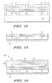
- FIG. 13 is a cross section view of another exemplary stackable package, consistent with one embodiment of the invention.
- FIG. 14 is a cross section view of an exemplary package-on-package structure, consistent with one embodiment of the invention.
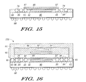
- FIG. 15 is a cross section view of an exemplary stackable package with a shield, consistent with one embodiment of the invention.
- FIG. 16 is a cross section view of another exemplary package-on-package structure, consistent with one embodiment of the invention.
- an exemplary method for forming a stackable package such as a packaged integrated circuit.
- the exemplary method may include providing a package substrate having a first surface, a first IC die attached to the first surface, a plurality of conductive members on the first surface at least partially surrounding the first IC die and electrically connected to the first IC die, and a dam on the first surface at least partially surrounding the plurality of conductive members.
- the exemplary method may further include performing a surface fill by providing an encapsulant to the first surface of the package substrate wherein the encapsulant surrounds the first IC die and is at least partially contained by the dam and wherein portions of each of the plurality of conductive members remain exposed during the surface fill.
- the method may include providing a package substrate having a first surface, a first IC die attached to the first surface, a plurality of conductive members on the first surface at least partially surrounding the first IC die and electrically connected to the first IC die.
- the method may further include providing a protection plate in physical contact with a top portion of each of the plurality of conductive members.
- the method may further include providing an encapsulant onto the first surface of the package substrate, wherein the encapsulant surrounds the first IC die and each of the plurality of conductive members, and wherein the protection plate remains in physical contact with the top portion of each of the plurality of conductive members during the providing the encapsulant.
- the method may further include removing the protection plate, wherein after removing the protection plate, the top portion of each of the plurality of conductive members remains exposed.
- a packaged integrated circuit may include a first packaged IC having a package substrate, at least one IC die attached to a first surface of the package substrate, a plurality of conductive members on the first surface at least partially surrounding the at least one IC die and electrically connected to the at least one IC die, an encapsulant over the first surface surrounding the at least one IC die and the plurality of conductive members, wherein at least a portion of each of the plurality of conductive members is exposed by the encapsulant.
- the packaged integrated circuit may further include a second packaged IC stacked onto the first packaged IC, the second packaged IC having at least one IC die and a plurality of conductive members electrically connected to the at least one IC die of the second packaged IC, each conductive member of the plurality of conductive members of the second packaged IC in contact with a corresponding conductive member of the plurality of conductive members of the first packaged IC.
- FIG. 1 is a top view of an exemplary substrate strip, consistent with one embodiment of the invention.
- a substrate strip 10 may be formed, which may include multiple substrate units.
- Substrate strip 10 may include die attach areas 16 , to which die could be attached later.
- Substrate strip 10 may further include bond posts 18 for wire bonding die.
- FIG. 1 shows bond posts 18 for wire bonding die, die may be connected to substrate strip 10 using other techniques, such as flip chip bonding.
- Substrate strip 10 may further include contact pads 20 for connecting stackable packages. Although FIG. 1 shows two rows/columns of contact pads 20 additional or fewer rows/columns may also be used.
- Substrate strip 10 may further include dam bars 12 and 14 .
- Dam bars 12 and 14 may be used to stop the flow of an encapsulant material beyond the periphery of the stackable package. Dam bars 12 and 14 may be formed by depositing solder balls on a copper strip. Alternatively, dam bars 12 and 14 may be formed by depositing any suitable dam bar material, including conductive or non-conductive materials. Furthermore, additional bars, such as bars 13 and 15 may be formed by depositing suitable dam bar material. Bars 13 and 15 may serve as a radio frequency shield for a die attached to die attach areas 16 . Additionally and/or alternatively, bars 13 and 15 may serve to shield the die from interference, such as electromagnetic interference. Also, shown in FIG.
- FIG. 1 is the direction 22 of saw-street along which substrate strip 10 may be singulated.
- FIG. 1 refers to a substrate strip 10 having a row of substrate of units, an array of substrate units with more than one row of substrate units may also be used.
- die 24 may be wire bonded to substrate strip 10 using bond posts 18 and wires 19 .
- FIG. 3 is a cross section view of the exemplary substrate of FIG. 2 with dams, shielding bars, and conductive balls, consistent with one embodiment of the invention.
- dams 26 , shielding supports 31 , and conductive balls 30 may be formed by re-flowing conductive material. Dams 26 (which may be formed using conductive balls), conductive balls 30 , and shielding supports may be preformed and may be attached to respective contact areas.
- FIG. 4 is a cross section view of the exemplary substrate of FIG. 3 with the encapsulant dispensed between dams, consistent with one embodiment of the invention.
- an encapsulant 34 may be dispensed on the top surface of substrate strip 10 using dispensers 32 , for example. Dams 26 may prevent the flow of encapsulant 34 beyond the periphery of the stackable packages. Any conventional encapsulants may be used as part of this step.
- External conductive balls 36 may be formed on a bottom surface of substrate strip 10 . Alternatively, preformed external conductive balls 36 may be attached to the bottom surface of substrate strip 10 .
- flip chip die 38 may also be used as part of stackable packages.
- Encapsulant 34 may act as an underfill between flip chip die 38 and a top surface of substrate strip 10 .
- stackable packages may be singulated. Die may be attached to substrate strip 10 using processes other than wire bonding and flip chip bonding.
- FIG. 6 is a top view of an exemplary top mold chase with vacuum-assisted pad protectors, consistent with one embodiment of the invention, which may be used as part of the molding process.
- Top mold chase 50 may include vacuum-assisted pad protectors 52 located in vacuum housing 51 .
- Vacuum housing 51 may be of the same material as the material of top mold chase 50 .
- inserts could be added to vacuum-assisted pad protectors 52 or to vacuum housing 51 in order to, for example, narrow the area covered by vacuum-assisted pad protectors 52 resulting in a variable pad width.
- Top mold chase 50 may further include a vacuum tube 54 .
- Top mold chase 50 may further include a mold injecting tube 56 . Molding material may be injected using mold injecting tube 56 .
- FIG. 7 a cross section view of a substrate inside a mold chase is shown.
- Substrate 60 including a die 62 attached to it, may be held between top mold chase 50 and bottom mold chase 58 .
- Molding material 64 (shown in FIG. 8 ) may be injected using mold injecting tube 56 .
- Vacuum tube 54 may be used to prevent the molding material from flowing into an area above contact pads 66 .
- a positive pressure may be applied through vacuum-assisted pad protectors 52 to prevent the molding material from flowing into an area above contact pads 66 .
- the application of positive pressure and/or vacuum could be controlled during the molding process to prevent overflow on the contact pads 66 .
- molding material 64 is shown as filling the area between top mold chase 50 and substrate 60 , except the area occupied by die 62 and the area protected by vacuum-assisted pad protectors 52 .
- FIG. 9 is a cross section view of an exemplary stackable package, consistent with one embodiment of the invention.
- Stackable package may include die 62 attached to substrate 60 with molding material 64 on top.
- Stackable package may further include conductive material 68 filled into the area protected by vacuum-assisted pad protectors 52 .
- Conductive material 68 may be filled using conventional processes and then leveled using a solder squeegee, for example.
- Conductive material 68 may be reflowed and the stackable package grinded, if necessary. Solder balls may also be inserted in the area above contact pads 66 , which could then be reflowed to form conductive material 68 .
- external conductive balls 63 may be formed on a bottom surface of substrate 60 for connecting the stackable package to other packages or other components, such as printed circuit boards.
- FIG. 9 shows die 62 as being wire bonded to substrate 60
- die 62 may be attached to substrate 60 using other techniques, such as flip chip bonding.
- stackable packages may be formed using other exemplary mold processes, as well. For example, as described below, a mold chase with a conductive ball protection plate may also be used to form stackable packages.
- a top mold chase 70 may include a conductive ball protection plate 72 .
- Top mold chase 70 may further include a mold injection tube 76 .
- FIG. 11 a cross section view of a substrate 80 inside a mold chase is shown.
- Substrate 80 including a die 82 attached to it, may be held between top mold chase 70 and bottom mold chase 78 .
- Molding material 86 (shown in FIG. 12 ) may be injected using mold injecting tube 76 .
- Alignment indentations 73 formed in conductive ball protection plate 72 may cover the top portion of conductive balls 74 to prevent the flow of molding material 86 on top of conductive balls 74 .
- conductive ball protection plate 72 may be removed subsequent to the injection of molding material, a top portion of conductive balls 74 may remain exposed.
- conductive ball protection plate 72 may be connected to top molding plate 70 using springs 77 .
- Springs 77 may provide pressure to conductive ball protection plate 72 to ensure that conductive ball protection plate 72 is not pushed up by molding material 86 .
- molding material 86 is shown as filling the area between conductive ball protection plate 72 and substrate 80 , except the area occupied by die 82 . Molding material 86 is also shown as an underfill for die 82 .
- FIG. 13 is a cross section view of an exemplary stackable package, consistent with one embodiment of the invention.
- Stackable package may include die 82 attached to substrate 80 with molding material 86 on top.
- Stackable package may further include conductive balls 74 , whose top portion is not covered by molding material 86 and is thus exposed.
- external conductive balls 88 may be formed on a bottom surface of substrate 80 for connecting the stackable package to other packages or other components, such as printed circuit boards.
- FIG. 13 shows die 82 as being flip chip bonded to substrate 80 , die 82 may be attached to substrate 80 using other techniques, such as wire bonding.
- FIG. 14 is a cross section view of an exemplary package-on-package structure 100 , consistent with one embodiment of the invention.
- a package-on-package (POP) structure 100 may be formed by stacking multiple packages.
- POP structure 100 may include a top package 90 over another stackable package.
- Package 90 may include die 92 and die 94 encapsulated in an encapsulant 98 .
- Package 90 may further include connecting pads 96 for connecting package 90 to another package.
- conductive balls 74 may be connected to connecting pads 96 to connect package 90 to another stackable package. Any stackable package described above may be used as part of POP structure 100 .
- a stackable package may also be stacked on top of the stackable package. Furthermore, any number of packages and/or stackable packages may be stacked on top of each other. Each package and/or stackable package may include one or more die. External conductive balls 88 may be formed on a bottom or top surface of any package, as and when necessary.
- FIG. 15 is a cross section view of another exemplary stackable package, consistent with one embodiment of the invention.
- Stackable package may include die 82 attached to substrate 80 with molding material 86 on top.
- Stackable package may further include conductive balls 74 , whose top portion is not covered by molding material 86 and is thus exposed.
- external conductive balls 88 may be formed on a bottom surface of substrate 80 for connecting the stackable package to other packages or other components, such as printed circuit boards.
- FIG. 15 shows die 82 as being flip chip bonded to substrate 80 , die 82 may be attached to substrate 80 using other techniques, such as wire bonding.
- Stackable package may further include contact pads 85 with shielding support, such as contact balls 87 connected to contact pads 85 .
- a shield such as a radio frequency shield or an electromagnetic interference shield may be mounted on top of shielding support/contact balls 87 .
- FIG. 15 shows contact balls 87 as shielding support, other types of shielding support may also be used.
- FIG. 16 is a cross section view of another exemplary package-on-package structure 200 , consistent with one embodiment of the invention.
- a package-on-package (POP) structure 200 may be formed by stacking multiple packages.
- POP structure 200 may include a top package 90 over another stackable package.
- Package 90 may include die 92 and die 94 encapsulated in an encapsulant 98 .
- Package 90 may further include connecting pads 96 for connecting package 90 to another package.
- conductive balls 74 may be connected to connecting pads 96 to connect package 90 to another stackable package. Any stackable package described above may be used as part of POP structure 200 .
- package-on-package structure 200 may include a shield 91 , which may act as a radio frequency shield or an electromagnetic interference shield.
- shield 91 may act as a radio frequency shield or an electromagnetic interference shield.
- contact pads 93 on a top surface of bottom package may be formed, which may then have a shielding support, such as contact balls 95 mounted thereon. Shield 91 may then be attached to contact balls 95 .
- FIG. 16 shows contact balls 95 as shielding support, other types of shielding support may also be used.
- Contact balls 87 and 95 acting as shielding support, may be electrically connected through the substrate to balls 88 which can be grounded to the desired locations.
Landscapes
- Structures Or Materials For Encapsulating Or Coating Semiconductor Devices Or Solid State Devices (AREA)
- Encapsulation Of And Coatings For Semiconductor Or Solid State Devices (AREA)
Abstract
Description
Claims (17)
Priority Applications (1)
| Application Number | Priority Date | Filing Date | Title |
|---|---|---|---|
| US12/567,469 US8044494B2 (en) | 2005-12-16 | 2009-09-25 | Stackable molded packages and methods of making the same |
Applications Claiming Priority (3)
| Application Number | Priority Date | Filing Date | Title |
|---|---|---|---|
| US11/311,579 US20070141751A1 (en) | 2005-12-16 | 2005-12-16 | Stackable molded packages and methods of making the same |
| US11/968,873 US20080108179A1 (en) | 2005-12-16 | 2008-01-03 | Stackable molded packages and methods of making the same |
| US12/567,469 US8044494B2 (en) | 2005-12-16 | 2009-09-25 | Stackable molded packages and methods of making the same |
Related Parent Applications (1)
| Application Number | Title | Priority Date | Filing Date |
|---|---|---|---|
| US11/968,873 Division US20080108179A1 (en) | 2005-12-16 | 2008-01-03 | Stackable molded packages and methods of making the same |
Publications (2)
| Publication Number | Publication Date |
|---|---|
| US20100013065A1 US20100013065A1 (en) | 2010-01-21 |
| US8044494B2 true US8044494B2 (en) | 2011-10-25 |
Family
ID=38174159
Family Applications (3)
| Application Number | Title | Priority Date | Filing Date |
|---|---|---|---|
| US11/311,579 Abandoned US20070141751A1 (en) | 2005-12-16 | 2005-12-16 | Stackable molded packages and methods of making the same |
| US11/968,873 Abandoned US20080108179A1 (en) | 2005-12-16 | 2008-01-03 | Stackable molded packages and methods of making the same |
| US12/567,469 Expired - Lifetime US8044494B2 (en) | 2005-12-16 | 2009-09-25 | Stackable molded packages and methods of making the same |
Family Applications Before (2)
| Application Number | Title | Priority Date | Filing Date |
|---|---|---|---|
| US11/311,579 Abandoned US20070141751A1 (en) | 2005-12-16 | 2005-12-16 | Stackable molded packages and methods of making the same |
| US11/968,873 Abandoned US20080108179A1 (en) | 2005-12-16 | 2008-01-03 | Stackable molded packages and methods of making the same |
Country Status (5)
| Country | Link |
|---|---|
| US (3) | US20070141751A1 (en) |
| JP (1) | JP2009520366A (en) |
| KR (1) | KR20080077177A (en) |
| TW (1) | TW200802789A (en) |
| WO (1) | WO2007120282A2 (en) |
Cited By (8)
| Publication number | Priority date | Publication date | Assignee | Title |
|---|---|---|---|---|
| US20060138649A1 (en) * | 2002-10-08 | 2006-06-29 | Chippac, Inc. | Semiconductor multi-package module having inverted second package stacked over die-up flip-chip ball grid array (BGA) package |
| US20100200975A1 (en) * | 2009-02-12 | 2010-08-12 | Shinko Electric Industries Co., Ltd. | Semiconductor device and method of manufacturing the same, and electronic apparatus |
| US20110024889A1 (en) * | 2009-07-31 | 2011-02-03 | Hata William Y | Package architecture |
| US20120049348A1 (en) * | 2010-08-31 | 2012-03-01 | Samsung Electronics Co., Ltd. | Package having elastic members for vias, package on package comprising the same, and methods of fabricating the same |
| US20140084446A1 (en) * | 2012-09-24 | 2014-03-27 | Soojeoung PARK | Semiconductor package and semiconductor devices with the same |
| US9525129B2 (en) | 2010-03-31 | 2016-12-20 | Everspin Technologies, Inc. | Methods of manufacturing a magnetic field sensor |
| USRE46428E1 (en) | 2009-09-25 | 2017-06-06 | Everspin Technologies, Inc. | Three axis magnetic field sensor |
| US20180053753A1 (en) * | 2016-08-16 | 2018-02-22 | Freescale Semiconductor, Inc. | Stackable molded packages and methods of manufacture thereof |
Families Citing this family (62)
| Publication number | Priority date | Publication date | Assignee | Title |
|---|---|---|---|---|
| US7364945B2 (en) | 2005-03-31 | 2008-04-29 | Stats Chippac Ltd. | Method of mounting an integrated circuit package in an encapsulant cavity |
| US8359739B2 (en) * | 2007-06-27 | 2013-01-29 | Rf Micro Devices, Inc. | Process for manufacturing a module |
| US8959762B2 (en) | 2005-08-08 | 2015-02-24 | Rf Micro Devices, Inc. | Method of manufacturing an electronic module |
| US7768125B2 (en) | 2006-01-04 | 2010-08-03 | Stats Chippac Ltd. | Multi-chip package system |
| US7723146B2 (en) * | 2006-01-04 | 2010-05-25 | Stats Chippac Ltd. | Integrated circuit package system with image sensor system |
| US8704349B2 (en) * | 2006-02-14 | 2014-04-22 | Stats Chippac Ltd. | Integrated circuit package system with exposed interconnects |
| KR100885419B1 (en) * | 2006-04-26 | 2009-02-24 | 삼성전자주식회사 | Stacked Package Structure |
| US8409920B2 (en) * | 2007-04-23 | 2013-04-02 | Stats Chippac Ltd. | Integrated circuit package system for package stacking and method of manufacture therefor |
| JP5081578B2 (en) * | 2007-10-25 | 2012-11-28 | ローム株式会社 | Resin-sealed semiconductor device |
| US8779570B2 (en) * | 2008-03-19 | 2014-07-15 | Stats Chippac Ltd. | Stackable integrated circuit package system |
| JP5185062B2 (en) * | 2008-10-21 | 2013-04-17 | パナソニック株式会社 | Multilayer semiconductor device and electronic device |
| KR101461630B1 (en) * | 2008-11-06 | 2014-11-20 | 삼성전자주식회사 | Wafer level chip on chip package, package on package improving solder joint reliability but reducing mounting height and manufacturing method thereof |
| CN102246262A (en) * | 2008-11-17 | 2011-11-16 | 派希斯系统整合私人有限公司 | Method for encapsulating semiconductor dies |
| US8130512B2 (en) * | 2008-11-18 | 2012-03-06 | Stats Chippac Ltd. | Integrated circuit package system and method of package stacking |
| US8102032B1 (en) * | 2008-12-09 | 2012-01-24 | Amkor Technology, Inc. | System and method for compartmental shielding of stacked packages |
| WO2010070806A1 (en) * | 2008-12-16 | 2010-06-24 | パナソニック株式会社 | Semiconductor device, flip-chip mounting method and flip-chip mounting apparatus |
| CN101924041B (en) * | 2009-06-16 | 2015-05-13 | 飞思卡尔半导体公司 | Method for assembling stackable semiconductor packaging |
| US8531012B2 (en) * | 2009-10-23 | 2013-09-10 | Stats Chippac, Ltd. | Semiconductor device and method of forming a shielding layer over a semiconductor die disposed in a cavity of an interconnect structure and grounded through the die TSV |
| EP2506298A1 (en) | 2009-11-27 | 2012-10-03 | Sumitomo Bakelite Company Limited | Production method for electronic device, electronic device, production method for electronic device package, and electronic device package |
| TWI497679B (en) * | 2009-11-27 | 2015-08-21 | 日月光半導體製造股份有限公司 | Semiconductor package and method of manufacturing same |
| US8569894B2 (en) | 2010-01-13 | 2013-10-29 | Advanced Semiconductor Engineering, Inc. | Semiconductor package with single sided substrate design and manufacturing methods thereof |
| US8314486B2 (en) * | 2010-02-23 | 2012-11-20 | Stats Chippac Ltd. | Integrated circuit packaging system with shield and method of manufacture thereof |
| US8299595B2 (en) * | 2010-03-18 | 2012-10-30 | Stats Chippac Ltd. | Integrated circuit package system with package stacking and method of manufacture thereof |
| TWI411075B (en) | 2010-03-22 | 2013-10-01 | 日月光半導體製造股份有限公司 | Semiconductor package and method of manufacturing same |
| US8569869B2 (en) * | 2010-03-23 | 2013-10-29 | Stats Chippac Ltd. | Integrated circuit packaging system with encapsulation and method of manufacture thereof |
| US9137934B2 (en) | 2010-08-18 | 2015-09-15 | Rf Micro Devices, Inc. | Compartmentalized shielding of selected components |
| US8546193B2 (en) * | 2010-11-02 | 2013-10-01 | Stats Chippac, Ltd. | Semiconductor device and method of forming penetrable film encapsulant around semiconductor die and interconnect structure |
| US8941222B2 (en) | 2010-11-11 | 2015-01-27 | Advanced Semiconductor Engineering Inc. | Wafer level semiconductor package and manufacturing methods thereof |
| US9406658B2 (en) | 2010-12-17 | 2016-08-02 | Advanced Semiconductor Engineering, Inc. | Embedded component device and manufacturing methods thereof |
| KR20120078390A (en) * | 2010-12-31 | 2012-07-10 | 삼성전자주식회사 | Stack type semiconductor package and method of fabricating the same |
| US8835226B2 (en) | 2011-02-25 | 2014-09-16 | Rf Micro Devices, Inc. | Connection using conductive vias |
| US9627230B2 (en) | 2011-02-28 | 2017-04-18 | Qorvo Us, Inc. | Methods of forming a microshield on standard QFN package |
| KR101222820B1 (en) | 2011-03-16 | 2013-01-15 | 삼성전기주식회사 | Semiconductor package and manufacturing method of the same |
| FR2977076A1 (en) * | 2011-06-21 | 2012-12-28 | St Microelectronics Grenoble 2 | SEMICONDUCTOR DEVICE WITH ENCAPSULATED ELECTRICAL CONNECTING ELEMENTS AND METHOD FOR MANUFACTURING THE SAME |
| JP2013069942A (en) * | 2011-09-24 | 2013-04-18 | Denso Corp | Semiconductor device and manufacturing method of the same |
| KR101798571B1 (en) | 2012-02-16 | 2017-11-16 | 삼성전자주식회사 | Semiconductor Packages |
| US9030841B2 (en) * | 2012-02-23 | 2015-05-12 | Apple Inc. | Low profile, space efficient circuit shields |
| TWI590399B (en) * | 2012-04-02 | 2017-07-01 | 矽品精密工業股份有限公司 | Semiconductor package and its manufacturing method and package substrate thereof |
| US8901730B2 (en) * | 2012-05-03 | 2014-12-02 | Taiwan Semiconductor Manufacturing Company, Ltd. | Methods and apparatus for package on package devices |
| US9385006B2 (en) * | 2012-06-21 | 2016-07-05 | STATS ChipPAC Pte. Ltd. | Semiconductor device and method of forming an embedded SOP fan-out package |
| US9538582B2 (en) * | 2012-07-26 | 2017-01-03 | Taiwan Semiconductor Manufacturing Company, Ltd. | Warpage control in the packaging of integrated circuits |
| JP2012256935A (en) * | 2012-08-31 | 2012-12-27 | Rohm Co Ltd | Resin sealing type semiconductor device |
| JP6016611B2 (en) * | 2012-12-20 | 2016-10-26 | 三菱電機株式会社 | Semiconductor module, manufacturing method thereof and connection method thereof |
| US9406596B2 (en) | 2013-02-21 | 2016-08-02 | Taiwan Semiconductor Manufacturing Company, Ltd. | Molding compound structure |
| JP6171402B2 (en) * | 2013-03-01 | 2017-08-02 | セイコーエプソン株式会社 | Modules, electronic devices, and mobile objects |
| US9807890B2 (en) | 2013-05-31 | 2017-10-31 | Qorvo Us, Inc. | Electronic modules having grounded electromagnetic shields |
| US9287240B2 (en) * | 2013-12-13 | 2016-03-15 | Micron Technology, Inc. | Stacked semiconductor die assemblies with thermal spacers and associated systems and methods |
| WO2015099781A1 (en) * | 2013-12-27 | 2015-07-02 | xyINTEL CORPORATION | Optoelectronic packaging assemblies |
| US9793242B2 (en) * | 2013-12-30 | 2017-10-17 | Taiwan Semiconductor Manufacturing Company, Ltd. | Packages with die stack including exposed molding underfill |
| WO2016043761A1 (en) | 2014-09-18 | 2016-03-24 | Intel Corporation | Method of embedding wlcsp components in e-wlb and e-plb |
| JP6093093B2 (en) * | 2015-01-22 | 2017-03-08 | 新電元工業株式会社 | Semiconductor module |
| KR102412611B1 (en) * | 2015-08-03 | 2022-06-23 | 삼성전자주식회사 | Printed Circuit Board(PCB), method for fabricating the PCB, and method for fabricating semiconductor package using the PCB |
| KR101712288B1 (en) * | 2015-11-12 | 2017-03-03 | 앰코 테크놀로지 코리아 주식회사 | Package of semiconductor and method for manufacturing the same |
| KR101837511B1 (en) * | 2016-04-04 | 2018-03-14 | 주식회사 네패스 | Semiconductor package and method of manufacturing the same |
| CN108780790B (en) * | 2017-01-04 | 2020-10-27 | 华为技术有限公司 | Stack packaging structure and terminal |
| WO2019005110A1 (en) * | 2017-06-30 | 2019-01-03 | Intel Corporation | Dual strip backside metallization for improved alt-fli plating, koz minimization, text enhancement and warpage control |
| US11127689B2 (en) | 2018-06-01 | 2021-09-21 | Qorvo Us, Inc. | Segmented shielding using wirebonds |
| US11219144B2 (en) | 2018-06-28 | 2022-01-04 | Qorvo Us, Inc. | Electromagnetic shields for sub-modules |
| US11114363B2 (en) | 2018-12-20 | 2021-09-07 | Qorvo Us, Inc. | Electronic package arrangements and related methods |
| US11515282B2 (en) | 2019-05-21 | 2022-11-29 | Qorvo Us, Inc. | Electromagnetic shields with bonding wires for sub-modules |
| IT202000001822A1 (en) | 2020-01-30 | 2021-07-30 | St Microelectronics Srl | INTEGRATED CIRCUIT AND ELECTRONIC DEVICE INCLUDING A PLURALITY OF INTEGRATED CIRCUITS ELECTRICALLY COUPLED VIA A SYNCHRONIZATION SIGNAL INSTRUCTED THROUGH THE INTEGRATED CIRCUIT |
| IT202000001819A1 (en) * | 2020-01-30 | 2021-07-30 | St Microelectronics Srl | INTEGRATED CIRCUIT AND ELECTRONIC DEVICE INCLUDING A PLURALITY OF INTEGRATED CIRCUITS ELECTRICALLY COUPLED VIA A SYNCHRONIZATION SIGNAL |
Citations (20)
| Publication number | Priority date | Publication date | Assignee | Title |
|---|---|---|---|---|
| US5153379A (en) | 1990-10-09 | 1992-10-06 | Motorola, Inc. | Shielded low-profile electronic component assembly |
| US5220489A (en) | 1991-10-11 | 1993-06-15 | Motorola, Inc. | Multicomponent integrated circuit package |
| US5222014A (en) | 1992-03-02 | 1993-06-22 | Motorola, Inc. | Three-dimensional multi-chip pad array carrier |
| US5311059A (en) | 1992-01-24 | 1994-05-10 | Motorola, Inc. | Backplane grounding for flip-chip integrated circuit |
| US5405808A (en) | 1993-08-16 | 1995-04-11 | Lsi Logic Corporation | Fluid-filled and gas-filled semiconductor packages |
| US5650659A (en) | 1995-08-04 | 1997-07-22 | National Semiconductor Corporation | Semiconductor component package assembly including an integral RF/EMI shield |
| US5891753A (en) | 1997-01-24 | 1999-04-06 | Micron Technology, Inc. | Method and apparatus for packaging flip chip bare die on printed circuit boards |
| US6007317A (en) | 1997-07-23 | 1999-12-28 | Micron Technology, Inc. | Ball grid array (BGA) encapsulation mold |
| US6291259B1 (en) | 1998-05-30 | 2001-09-18 | Hyundai Electronics Industries Co., Ltd. | Stackable ball grid array semiconductor package and fabrication method thereof |
| US6707168B1 (en) * | 2001-05-04 | 2004-03-16 | Amkor Technology, Inc. | Shielded semiconductor package with single-sided substrate and method for making the same |
| US20040065473A1 (en) | 2002-10-08 | 2004-04-08 | Siliconware Precision Industries, Ltd., Taiwan | Warpage preventing substrate |
| US20040207064A1 (en) | 1998-09-03 | 2004-10-21 | Brooks Jerry M. | Cavity ball grid array apparatus having improved inductance characteristics |
| US20040212066A1 (en) | 2003-04-23 | 2004-10-28 | Advanced Semiconductor Engineering, Inc. | Multi-chips stacked package |
| US6815254B2 (en) | 2003-03-10 | 2004-11-09 | Freescale Semiconductor, Inc. | Semiconductor package with multiple sides having package contacts |
| US20050093152A1 (en) | 2003-10-10 | 2005-05-05 | Fjelstad Joseph C. | Multi-surface contact IC packaging structures and assemblies |
| US20050164429A1 (en) | 2000-06-02 | 2005-07-28 | Kinsman Larry D. | Method for fabricating a chip scale package using wafer level processing |
| US6933598B2 (en) * | 2002-10-08 | 2005-08-23 | Chippac, Inc. | Semiconductor stacked multi-package module having inverted second package and electrically shielded first package |
| US7537962B2 (en) * | 2006-12-22 | 2009-05-26 | Stats Chippac Ltd. | Method of fabricating a shielded stacked integrated circuit package system |
| US7642133B2 (en) * | 2006-09-27 | 2010-01-05 | Advanced Semiconductor Engineering, Inc. | Method of making a semiconductor package and method of making a semiconductor device |
| US7851894B1 (en) * | 2008-12-23 | 2010-12-14 | Amkor Technology, Inc. | System and method for shielding of package on package (PoP) assemblies |
-
2005
- 2005-12-16 US US11/311,579 patent/US20070141751A1/en not_active Abandoned
-
2006
- 2006-11-21 WO PCT/US2006/061127 patent/WO2007120282A2/en not_active Ceased
- 2006-11-21 KR KR1020087014218A patent/KR20080077177A/en not_active Withdrawn
- 2006-11-21 JP JP2008545899A patent/JP2009520366A/en active Pending
- 2006-11-27 TW TW095143749A patent/TW200802789A/en unknown
-
2008
- 2008-01-03 US US11/968,873 patent/US20080108179A1/en not_active Abandoned
-
2009
- 2009-09-25 US US12/567,469 patent/US8044494B2/en not_active Expired - Lifetime
Patent Citations (20)
| Publication number | Priority date | Publication date | Assignee | Title |
|---|---|---|---|---|
| US5153379A (en) | 1990-10-09 | 1992-10-06 | Motorola, Inc. | Shielded low-profile electronic component assembly |
| US5220489A (en) | 1991-10-11 | 1993-06-15 | Motorola, Inc. | Multicomponent integrated circuit package |
| US5311059A (en) | 1992-01-24 | 1994-05-10 | Motorola, Inc. | Backplane grounding for flip-chip integrated circuit |
| US5222014A (en) | 1992-03-02 | 1993-06-22 | Motorola, Inc. | Three-dimensional multi-chip pad array carrier |
| US5405808A (en) | 1993-08-16 | 1995-04-11 | Lsi Logic Corporation | Fluid-filled and gas-filled semiconductor packages |
| US5650659A (en) | 1995-08-04 | 1997-07-22 | National Semiconductor Corporation | Semiconductor component package assembly including an integral RF/EMI shield |
| US5891753A (en) | 1997-01-24 | 1999-04-06 | Micron Technology, Inc. | Method and apparatus for packaging flip chip bare die on printed circuit boards |
| US6007317A (en) | 1997-07-23 | 1999-12-28 | Micron Technology, Inc. | Ball grid array (BGA) encapsulation mold |
| US6291259B1 (en) | 1998-05-30 | 2001-09-18 | Hyundai Electronics Industries Co., Ltd. | Stackable ball grid array semiconductor package and fabrication method thereof |
| US20040207064A1 (en) | 1998-09-03 | 2004-10-21 | Brooks Jerry M. | Cavity ball grid array apparatus having improved inductance characteristics |
| US20050164429A1 (en) | 2000-06-02 | 2005-07-28 | Kinsman Larry D. | Method for fabricating a chip scale package using wafer level processing |
| US6707168B1 (en) * | 2001-05-04 | 2004-03-16 | Amkor Technology, Inc. | Shielded semiconductor package with single-sided substrate and method for making the same |
| US20040065473A1 (en) | 2002-10-08 | 2004-04-08 | Siliconware Precision Industries, Ltd., Taiwan | Warpage preventing substrate |
| US6933598B2 (en) * | 2002-10-08 | 2005-08-23 | Chippac, Inc. | Semiconductor stacked multi-package module having inverted second package and electrically shielded first package |
| US6815254B2 (en) | 2003-03-10 | 2004-11-09 | Freescale Semiconductor, Inc. | Semiconductor package with multiple sides having package contacts |
| US20040212066A1 (en) | 2003-04-23 | 2004-10-28 | Advanced Semiconductor Engineering, Inc. | Multi-chips stacked package |
| US20050093152A1 (en) | 2003-10-10 | 2005-05-05 | Fjelstad Joseph C. | Multi-surface contact IC packaging structures and assemblies |
| US7642133B2 (en) * | 2006-09-27 | 2010-01-05 | Advanced Semiconductor Engineering, Inc. | Method of making a semiconductor package and method of making a semiconductor device |
| US7537962B2 (en) * | 2006-12-22 | 2009-05-26 | Stats Chippac Ltd. | Method of fabricating a shielded stacked integrated circuit package system |
| US7851894B1 (en) * | 2008-12-23 | 2010-12-14 | Amkor Technology, Inc. | System and method for shielding of package on package (PoP) assemblies |
Non-Patent Citations (8)
| Title |
|---|
| Office Action on Related U.S. Appl. No. 11/311,579 mailed ~Apr. 27, 2007. |
| Office Action on Related U.S. Appl. No. 11/311,579 mailed ~Sep. 10, 2007. |
| Office Action on Related U.S. Appl. No. 11/311,579 mailed ˜Apr. 27, 2007. |
| Office Action on Related U.S. Appl. No. 11/311,579 mailed ˜Sep. 10, 2007. |
| Office Action on Related U.S. Appl. No. 11/968,873 mailed May 27, 2009. |
| Restriction on Related U.S. Appl. No. 11/311,579 mailed Mar. 27, 2007. |
| Restriction on Related U.S. Appl. No. 11/968,873 mailed Dec. 28, 2008. |
| Restriction on Related U.S. Appl. No. 11/968,873 mailed Mar. 3, 2009. |
Cited By (19)
| Publication number | Priority date | Publication date | Assignee | Title |
|---|---|---|---|---|
| US20060138649A1 (en) * | 2002-10-08 | 2006-06-29 | Chippac, Inc. | Semiconductor multi-package module having inverted second package stacked over die-up flip-chip ball grid array (BGA) package |
| US20100200975A1 (en) * | 2009-02-12 | 2010-08-12 | Shinko Electric Industries Co., Ltd. | Semiconductor device and method of manufacturing the same, and electronic apparatus |
| US8344492B2 (en) * | 2009-02-12 | 2013-01-01 | Shinko Electric Industries Co., Ltd. | Semiconductor device and method of manufacturing the same, and electronic apparatus |
| US20110024889A1 (en) * | 2009-07-31 | 2011-02-03 | Hata William Y | Package architecture |
| US8148813B2 (en) * | 2009-07-31 | 2012-04-03 | Altera Corporation | Integrated circuit package architecture |
| USRE46428E1 (en) | 2009-09-25 | 2017-06-06 | Everspin Technologies, Inc. | Three axis magnetic field sensor |
| USRE50684E1 (en) | 2009-09-25 | 2025-12-02 | Everspin Technologies, Inc. | Three axis magnetic field sensor |
| USRE49404E1 (en) | 2009-09-25 | 2023-01-31 | Everspin Technologies, Inc. | Three axis magnetic field sensor |
| US9893274B2 (en) | 2010-03-31 | 2018-02-13 | Everspin Technologies, Inc. | Methods of manufacturing a magnetic field sensor |
| US9525129B2 (en) | 2010-03-31 | 2016-12-20 | Everspin Technologies, Inc. | Methods of manufacturing a magnetic field sensor |
| US9553261B2 (en) | 2010-03-31 | 2017-01-24 | Everspin Technologies, Inc. | Methods of manufacturing a magnetic field sensor |
| US10276789B2 (en) | 2010-03-31 | 2019-04-30 | Everspin Technologies, Inc. | Methods of manufacturing a magnetic field sensor |
| US11024799B2 (en) | 2010-03-31 | 2021-06-01 | Everspin Technologies, Inc. | Methods of manufacturing a magnetic field sensor |
| US11678584B2 (en) | 2010-03-31 | 2023-06-13 | Everspin Technologies, Inc. | Methods of manufacturing a magnetic field sensor |
| US8274144B2 (en) * | 2010-08-31 | 2012-09-25 | Samsung Electronics Co., Ltd. | Helical springs electrical connecting a plurality of packages |
| US20120049348A1 (en) * | 2010-08-31 | 2012-03-01 | Samsung Electronics Co., Ltd. | Package having elastic members for vias, package on package comprising the same, and methods of fabricating the same |
| US9029989B2 (en) * | 2012-09-24 | 2015-05-12 | Samsung Electronics Co., Ltd. | Semiconductor package and semiconductor devices with the same |
| US20140084446A1 (en) * | 2012-09-24 | 2014-03-27 | Soojeoung PARK | Semiconductor package and semiconductor devices with the same |
| US20180053753A1 (en) * | 2016-08-16 | 2018-02-22 | Freescale Semiconductor, Inc. | Stackable molded packages and methods of manufacture thereof |
Also Published As
| Publication number | Publication date |
|---|---|
| WO2007120282A3 (en) | 2008-04-10 |
| WO2007120282A2 (en) | 2007-10-25 |
| KR20080077177A (en) | 2008-08-21 |
| US20100013065A1 (en) | 2010-01-21 |
| US20080108179A1 (en) | 2008-05-08 |
| JP2009520366A (en) | 2009-05-21 |
| TW200802789A (en) | 2008-01-01 |
| US20070141751A1 (en) | 2007-06-21 |
Similar Documents
| Publication | Publication Date | Title |
|---|---|---|
| US8044494B2 (en) | Stackable molded packages and methods of making the same | |
| US7399658B2 (en) | Pre-molded leadframe and method therefor | |
| US8409923B2 (en) | Integrated circuit packaging system with underfill and method of manufacture thereof | |
| US7262074B2 (en) | Methods of fabricating underfilled, encapsulated semiconductor die assemblies | |
| US6664615B1 (en) | Method and apparatus for lead-frame based grid array IC packaging | |
| US7759221B2 (en) | Methods for packaging microelectronic devices and microelectronic devices formed using such methods | |
| US20070273019A1 (en) | Semiconductor package, chip carrier structure thereof, and method for fabricating the chip carrier | |
| US20030211660A1 (en) | BOC BGA package for die with I-shaped bond pad layout | |
| US20030148557A1 (en) | BOC BGA package for die with I-shaped bond pad layout | |
| US20090017583A1 (en) | Double encapsulated semiconductor package and manufacturing method thereof | |
| KR20200106001A (en) | Control of sub-charge for double-sided ball grid array packages | |
| US11810839B2 (en) | Semiconductor package with die stacked on surface mounted devices | |
| US7190066B2 (en) | Heat spreader and package structure utilizing the same | |
| US9576873B2 (en) | Integrated circuit packaging system with routable trace and method of manufacture thereof | |
| US8124459B2 (en) | Bump chip carrier semiconductor package system | |
| KR100959957B1 (en) | Land grid array semiconductor device package, assembly and manufacturing method comprising the same | |
| US7763983B2 (en) | Stackable microelectronic device carriers, stacked device carriers and methods of making the same | |
| US8823170B2 (en) | Apparatus and method for three dimensional integrated circuits | |
| US8680663B2 (en) | Methods and apparatus for package on package devices with reduced strain | |
| KR100922370B1 (en) | Semiconductor package material | |
| US20090096070A1 (en) | Semiconductor package and substrate for the same | |
| US7763961B2 (en) | Hybrid stacking package system | |
| US20110039371A1 (en) | Flip chip cavity package | |
| KR20070069753A (en) | Semiconductor chip stack package and its packaging method |
Legal Events
| Date | Code | Title | Description |
|---|---|---|---|
| AS | Assignment |
Owner name: CITIBANK, N.A.,NEW YORK Free format text: SECURITY AGREEMENT;ASSIGNOR:FREESCALE SEMICONDUCTOR, INC.;REEL/FRAME:023882/0834 Effective date: 20091030 Owner name: CITIBANK, N.A., NEW YORK Free format text: SECURITY AGREEMENT;ASSIGNOR:FREESCALE SEMICONDUCTOR, INC.;REEL/FRAME:023882/0834 Effective date: 20091030 |
|
| AS | Assignment |
Owner name: CITIBANK, N.A.,NEW YORK Free format text: SECURITY AGREEMENT;ASSIGNOR:FREESCALE SEMICONDUCTOR, INC.;REEL/FRAME:024085/0001 Effective date: 20100219 Owner name: CITIBANK, N.A., NEW YORK Free format text: SECURITY AGREEMENT;ASSIGNOR:FREESCALE SEMICONDUCTOR, INC.;REEL/FRAME:024085/0001 Effective date: 20100219 |
|
| AS | Assignment |
Owner name: CITIBANK, N.A., AS COLLATERAL AGENT,NEW YORK Free format text: SECURITY AGREEMENT;ASSIGNOR:FREESCALE SEMICONDUCTOR, INC.;REEL/FRAME:024397/0001 Effective date: 20100413 Owner name: CITIBANK, N.A., AS COLLATERAL AGENT, NEW YORK Free format text: SECURITY AGREEMENT;ASSIGNOR:FREESCALE SEMICONDUCTOR, INC.;REEL/FRAME:024397/0001 Effective date: 20100413 |
|
| STCF | Information on status: patent grant |
Free format text: PATENTED CASE |
|
| AS | Assignment |
Owner name: CITIBANK, N.A., AS NOTES COLLATERAL AGENT, NEW YORK Free format text: SECURITY AGREEMENT;ASSIGNOR:FREESCALE SEMICONDUCTOR, INC.;REEL/FRAME:030633/0424 Effective date: 20130521 Owner name: CITIBANK, N.A., AS NOTES COLLATERAL AGENT, NEW YOR Free format text: SECURITY AGREEMENT;ASSIGNOR:FREESCALE SEMICONDUCTOR, INC.;REEL/FRAME:030633/0424 Effective date: 20130521 |
|
| AS | Assignment |
Owner name: CITIBANK, N.A., AS NOTES COLLATERAL AGENT, NEW YORK Free format text: SECURITY AGREEMENT;ASSIGNOR:FREESCALE SEMICONDUCTOR, INC.;REEL/FRAME:031591/0266 Effective date: 20131101 Owner name: CITIBANK, N.A., AS NOTES COLLATERAL AGENT, NEW YOR Free format text: SECURITY AGREEMENT;ASSIGNOR:FREESCALE SEMICONDUCTOR, INC.;REEL/FRAME:031591/0266 Effective date: 20131101 |
|
| FPAY | Fee payment |
Year of fee payment: 4 |
|
| AS | Assignment |
Owner name: FREESCALE SEMICONDUCTOR, INC., TEXAS Free format text: PATENT RELEASE;ASSIGNOR:CITIBANK, N.A., AS COLLATERAL AGENT;REEL/FRAME:037354/0854 Effective date: 20151207 Owner name: FREESCALE SEMICONDUCTOR, INC., TEXAS Free format text: PATENT RELEASE;ASSIGNOR:CITIBANK, N.A., AS COLLATERAL AGENT;REEL/FRAME:037356/0553 Effective date: 20151207 Owner name: FREESCALE SEMICONDUCTOR, INC., TEXAS Free format text: PATENT RELEASE;ASSIGNOR:CITIBANK, N.A., AS COLLATERAL AGENT;REEL/FRAME:037356/0143 Effective date: 20151207 |
|
| AS | Assignment |
Owner name: MORGAN STANLEY SENIOR FUNDING, INC., MARYLAND Free format text: ASSIGNMENT AND ASSUMPTION OF SECURITY INTEREST IN PATENTS;ASSIGNOR:CITIBANK, N.A.;REEL/FRAME:037486/0517 Effective date: 20151207 |
|
| AS | Assignment |
Owner name: MORGAN STANLEY SENIOR FUNDING, INC., MARYLAND Free format text: ASSIGNMENT AND ASSUMPTION OF SECURITY INTEREST IN PATENTS;ASSIGNOR:CITIBANK, N.A.;REEL/FRAME:037518/0292 Effective date: 20151207 |
|
| AS | Assignment |
Owner name: MORGAN STANLEY SENIOR FUNDING, INC., MARYLAND Free format text: SECURITY AGREEMENT SUPPLEMENT;ASSIGNOR:NXP B.V.;REEL/FRAME:038017/0058 Effective date: 20160218 |
|
| AS | Assignment |
Owner name: MORGAN STANLEY SENIOR FUNDING, INC., MARYLAND Free format text: SUPPLEMENT TO THE SECURITY AGREEMENT;ASSIGNOR:FREESCALE SEMICONDUCTOR, INC.;REEL/FRAME:039138/0001 Effective date: 20160525 |
|
| AS | Assignment |
Owner name: MORGAN STANLEY SENIOR FUNDING, INC., MARYLAND Free format text: CORRECTIVE ASSIGNMENT TO CORRECT THE REMOVE APPLICATION 12092129 PREVIOUSLY RECORDED ON REEL 038017 FRAME 0058. ASSIGNOR(S) HEREBY CONFIRMS THE SECURITY AGREEMENT SUPPLEMENT;ASSIGNOR:NXP B.V.;REEL/FRAME:039361/0212 Effective date: 20160218 |
|
| AS | Assignment |
Owner name: NXP, B.V., F/K/A FREESCALE SEMICONDUCTOR, INC., NETHERLANDS Free format text: RELEASE BY SECURED PARTY;ASSIGNOR:MORGAN STANLEY SENIOR FUNDING, INC.;REEL/FRAME:040925/0001 Effective date: 20160912 Owner name: NXP, B.V., F/K/A FREESCALE SEMICONDUCTOR, INC., NE Free format text: RELEASE BY SECURED PARTY;ASSIGNOR:MORGAN STANLEY SENIOR FUNDING, INC.;REEL/FRAME:040925/0001 Effective date: 20160912 |
|
| AS | Assignment |
Owner name: NXP B.V., NETHERLANDS Free format text: RELEASE BY SECURED PARTY;ASSIGNOR:MORGAN STANLEY SENIOR FUNDING, INC.;REEL/FRAME:040928/0001 Effective date: 20160622 |
|
| AS | Assignment |
Owner name: NXP USA, INC., TEXAS Free format text: CHANGE OF NAME;ASSIGNOR:FREESCALE SEMICONDUCTOR INC.;REEL/FRAME:040652/0180 Effective date: 20161107 |
|
| AS | Assignment |
Owner name: NXP USA, INC., TEXAS Free format text: CORRECTIVE ASSIGNMENT TO CORRECT THE NATURE OF CONVEYANCE LISTED CHANGE OF NAME SHOULD BE MERGER AND CHANGE PREVIOUSLY RECORDED AT REEL: 040652 FRAME: 0180. ASSIGNOR(S) HEREBY CONFIRMS THE MERGER AND CHANGE OF NAME;ASSIGNOR:FREESCALE SEMICONDUCTOR INC.;REEL/FRAME:041354/0148 Effective date: 20161107 |
|
| AS | Assignment |
Owner name: MORGAN STANLEY SENIOR FUNDING, INC., MARYLAND Free format text: CORRECTIVE ASSIGNMENT TO CORRECT THE REMOVE PATENTS 8108266 AND 8062324 AND REPLACE THEM WITH 6108266 AND 8060324 PREVIOUSLY RECORDED ON REEL 037518 FRAME 0292. ASSIGNOR(S) HEREBY CONFIRMS THE ASSIGNMENT AND ASSUMPTION OF SECURITY INTEREST IN PATENTS;ASSIGNOR:CITIBANK, N.A.;REEL/FRAME:041703/0536 Effective date: 20151207 |
|
| AS | Assignment |
Owner name: MORGAN STANLEY SENIOR FUNDING, INC., MARYLAND Free format text: CORRECTIVE ASSIGNMENT TO CORRECT THE REMOVE APPLICATION 12681366 PREVIOUSLY RECORDED ON REEL 039361 FRAME 0212. ASSIGNOR(S) HEREBY CONFIRMS THE SECURITY AGREEMENT SUPPLEMENT;ASSIGNOR:NXP B.V.;REEL/FRAME:042762/0145 Effective date: 20160218 Owner name: MORGAN STANLEY SENIOR FUNDING, INC., MARYLAND Free format text: CORRECTIVE ASSIGNMENT TO CORRECT THE REMOVE APPLICATION 12681366 PREVIOUSLY RECORDED ON REEL 038017 FRAME 0058. ASSIGNOR(S) HEREBY CONFIRMS THE SECURITY AGREEMENT SUPPLEMENT;ASSIGNOR:NXP B.V.;REEL/FRAME:042985/0001 Effective date: 20160218 |
|
| AS | Assignment |
Owner name: SHENZHEN XINGUODU TECHNOLOGY CO., LTD., CHINA Free format text: CORRECTIVE ASSIGNMENT TO CORRECT THE TO CORRECT THE APPLICATION NO. FROM 13,883,290 TO 13,833,290 PREVIOUSLY RECORDED ON REEL 041703 FRAME 0536. ASSIGNOR(S) HEREBY CONFIRMS THE THE ASSIGNMENT AND ASSUMPTION OF SECURITYINTEREST IN PATENTS.;ASSIGNOR:MORGAN STANLEY SENIOR FUNDING, INC.;REEL/FRAME:048734/0001 Effective date: 20190217 Owner name: SHENZHEN XINGUODU TECHNOLOGY CO., LTD., CHINA Free format text: CORRECTIVE ASSIGNMENT TO CORRECT THE TO CORRECT THE APPLICATION NO. FROM 13,883,290 TO 13,833,290 PREVIOUSLY RECORDED ON REEL 041703 FRAME 0536. ASSIGNOR(S) HEREBY CONFIRMS THE THE ASSIGNMENT AND ASSUMPTION OF SECURITY INTEREST IN PATENTS.;ASSIGNOR:MORGAN STANLEY SENIOR FUNDING, INC.;REEL/FRAME:048734/0001 Effective date: 20190217 |
|
| MAFP | Maintenance fee payment |
Free format text: PAYMENT OF MAINTENANCE FEE, 8TH YEAR, LARGE ENTITY (ORIGINAL EVENT CODE: M1552); ENTITY STATUS OF PATENT OWNER: LARGE ENTITY Year of fee payment: 8 |
|
| AS | Assignment |
Owner name: NXP B.V., NETHERLANDS Free format text: RELEASE BY SECURED PARTY;ASSIGNOR:MORGAN STANLEY SENIOR FUNDING, INC.;REEL/FRAME:050745/0001 Effective date: 20190903 Owner name: NXP B.V., NETHERLANDS Free format text: RELEASE BY SECURED PARTY;ASSIGNOR:MORGAN STANLEY SENIOR FUNDING, INC.;REEL/FRAME:050744/0097 Effective date: 20190903 |
|
| AS | Assignment |
Owner name: MORGAN STANLEY SENIOR FUNDING, INC., MARYLAND Free format text: CORRECTIVE ASSIGNMENT TO CORRECT THE REMOVE APPLICATION 12298143 PREVIOUSLY RECORDED ON REEL 042985 FRAME 0001. ASSIGNOR(S) HEREBY CONFIRMS THE SECURITY AGREEMENT SUPPLEMENT;ASSIGNOR:NXP B.V.;REEL/FRAME:051029/0001 Effective date: 20160218 Owner name: MORGAN STANLEY SENIOR FUNDING, INC., MARYLAND Free format text: CORRECTIVE ASSIGNMENT TO CORRECT THE REMOVE APPLICATION 12298143 PREVIOUSLY RECORDED ON REEL 042762 FRAME 0145. ASSIGNOR(S) HEREBY CONFIRMS THE SECURITY AGREEMENT SUPPLEMENT;ASSIGNOR:NXP B.V.;REEL/FRAME:051145/0184 Effective date: 20160218 Owner name: MORGAN STANLEY SENIOR FUNDING, INC., MARYLAND Free format text: CORRECTIVE ASSIGNMENT TO CORRECT THE REMOVE APPLICATION 12298143 PREVIOUSLY RECORDED ON REEL 039361 FRAME 0212. ASSIGNOR(S) HEREBY CONFIRMS THE SECURITY AGREEMENT SUPPLEMENT;ASSIGNOR:NXP B.V.;REEL/FRAME:051029/0387 Effective date: 20160218 Owner name: MORGAN STANLEY SENIOR FUNDING, INC., MARYLAND Free format text: CORRECTIVE ASSIGNMENT TO CORRECT THE REMOVE APPLICATION12298143 PREVIOUSLY RECORDED ON REEL 039361 FRAME 0212. ASSIGNOR(S) HEREBY CONFIRMS THE SECURITY AGREEMENT SUPPLEMENT;ASSIGNOR:NXP B.V.;REEL/FRAME:051029/0387 Effective date: 20160218 Owner name: MORGAN STANLEY SENIOR FUNDING, INC., MARYLAND Free format text: CORRECTIVE ASSIGNMENT TO CORRECT THE REMOVE APPLICATION 12298143 PREVIOUSLY RECORDED ON REEL 038017 FRAME 0058. ASSIGNOR(S) HEREBY CONFIRMS THE SECURITY AGREEMENT SUPPLEMENT;ASSIGNOR:NXP B.V.;REEL/FRAME:051030/0001 Effective date: 20160218 Owner name: MORGAN STANLEY SENIOR FUNDING, INC., MARYLAND Free format text: CORRECTIVE ASSIGNMENT TO CORRECT THE REMOVE APPLICATION12298143 PREVIOUSLY RECORDED ON REEL 042985 FRAME 0001. ASSIGNOR(S) HEREBY CONFIRMS THE SECURITY AGREEMENT SUPPLEMENT;ASSIGNOR:NXP B.V.;REEL/FRAME:051029/0001 Effective date: 20160218 Owner name: MORGAN STANLEY SENIOR FUNDING, INC., MARYLAND Free format text: CORRECTIVE ASSIGNMENT TO CORRECT THE REMOVE APPLICATION12298143 PREVIOUSLY RECORDED ON REEL 042762 FRAME 0145. ASSIGNOR(S) HEREBY CONFIRMS THE SECURITY AGREEMENT SUPPLEMENT;ASSIGNOR:NXP B.V.;REEL/FRAME:051145/0184 Effective date: 20160218 |
|
| AS | Assignment |
Owner name: MORGAN STANLEY SENIOR FUNDING, INC., MARYLAND Free format text: CORRECTIVE ASSIGNMENT TO CORRECT THE REMOVE APPLICATION11759915 AND REPLACE IT WITH APPLICATION 11759935 PREVIOUSLY RECORDED ON REEL 037486 FRAME 0517. ASSIGNOR(S) HEREBY CONFIRMS THE ASSIGNMENT AND ASSUMPTION OF SECURITYINTEREST IN PATENTS;ASSIGNOR:CITIBANK, N.A.;REEL/FRAME:053547/0421 Effective date: 20151207 Owner name: MORGAN STANLEY SENIOR FUNDING, INC., MARYLAND Free format text: CORRECTIVE ASSIGNMENT TO CORRECT THE REMOVE APPLICATION 11759915 AND REPLACE IT WITH APPLICATION 11759935 PREVIOUSLY RECORDED ON REEL 037486 FRAME 0517. ASSIGNOR(S) HEREBY CONFIRMS THE ASSIGNMENT AND ASSUMPTION OF SECURITY INTEREST IN PATENTS;ASSIGNOR:CITIBANK, N.A.;REEL/FRAME:053547/0421 Effective date: 20151207 |
|
| AS | Assignment |
Owner name: NXP B.V., NETHERLANDS Free format text: CORRECTIVE ASSIGNMENT TO CORRECT THE REMOVEAPPLICATION 11759915 AND REPLACE IT WITH APPLICATION11759935 PREVIOUSLY RECORDED ON REEL 040928 FRAME 0001. ASSIGNOR(S) HEREBY CONFIRMS THE RELEASE OF SECURITYINTEREST;ASSIGNOR:MORGAN STANLEY SENIOR FUNDING, INC.;REEL/FRAME:052915/0001 Effective date: 20160622 Owner name: NXP B.V., NETHERLANDS Free format text: CORRECTIVE ASSIGNMENT TO CORRECT THE REMOVE APPLICATION 11759915 AND REPLACE IT WITH APPLICATION 11759935 PREVIOUSLY RECORDED ON REEL 040928 FRAME 0001. ASSIGNOR(S) HEREBY CONFIRMS THE RELEASE OF SECURITY INTEREST;ASSIGNOR:MORGAN STANLEY SENIOR FUNDING, INC.;REEL/FRAME:052915/0001 Effective date: 20160622 |
|
| AS | Assignment |
Owner name: NXP, B.V. F/K/A FREESCALE SEMICONDUCTOR, INC., NETHERLANDS Free format text: CORRECTIVE ASSIGNMENT TO CORRECT THE REMOVEAPPLICATION 11759915 AND REPLACE IT WITH APPLICATION11759935 PREVIOUSLY RECORDED ON REEL 040925 FRAME 0001. ASSIGNOR(S) HEREBY CONFIRMS THE RELEASE OF SECURITYINTEREST;ASSIGNOR:MORGAN STANLEY SENIOR FUNDING, INC.;REEL/FRAME:052917/0001 Effective date: 20160912 Owner name: NXP, B.V. F/K/A FREESCALE SEMICONDUCTOR, INC., NETHERLANDS Free format text: CORRECTIVE ASSIGNMENT TO CORRECT THE REMOVE APPLICATION 11759915 AND REPLACE IT WITH APPLICATION 11759935 PREVIOUSLY RECORDED ON REEL 040925 FRAME 0001. ASSIGNOR(S) HEREBY CONFIRMS THE RELEASE OF SECURITY INTEREST;ASSIGNOR:MORGAN STANLEY SENIOR FUNDING, INC.;REEL/FRAME:052917/0001 Effective date: 20160912 |
|
| MAFP | Maintenance fee payment |
Free format text: PAYMENT OF MAINTENANCE FEE, 12TH YEAR, LARGE ENTITY (ORIGINAL EVENT CODE: M1553); ENTITY STATUS OF PATENT OWNER: LARGE ENTITY Year of fee payment: 12 |