US8044458B2 - Semiconductor device including a vertical gate zone, and method for producing the same - Google Patents
Semiconductor device including a vertical gate zone, and method for producing the same Download PDFInfo
- Publication number
- US8044458B2 US8044458B2 US11/752,590 US75259007A US8044458B2 US 8044458 B2 US8044458 B2 US 8044458B2 US 75259007 A US75259007 A US 75259007A US 8044458 B2 US8044458 B2 US 8044458B2
- Authority
- US
- United States
- Prior art keywords
- zone
- zones
- dopant
- drift
- gate
- Prior art date
- Legal status (The legal status is an assumption and is not a legal conclusion. Google has not performed a legal analysis and makes no representation as to the accuracy of the status listed.)
- Expired - Fee Related
Links
- 239000004065 semiconductor Substances 0.000 title claims abstract description 120
- 238000004519 manufacturing process Methods 0.000 title claims description 5
- 239000002019 doping agent Substances 0.000 claims abstract description 80
- 239000012535 impurity Substances 0.000 claims abstract description 12
- 230000000295 complement effect Effects 0.000 claims abstract description 6
- 238000000034 method Methods 0.000 claims description 23
- RQNWIZPPADIBDY-UHFFFAOYSA-N arsenic atom Chemical group [As] RQNWIZPPADIBDY-UHFFFAOYSA-N 0.000 claims description 10
- 238000002513 implantation Methods 0.000 claims description 9
- 230000015556 catabolic process Effects 0.000 claims description 8
- XUIMIQQOPSSXEZ-UHFFFAOYSA-N Silicon Chemical compound [Si] XUIMIQQOPSSXEZ-UHFFFAOYSA-N 0.000 claims description 7
- 229910052710 silicon Inorganic materials 0.000 claims description 7
- 239000010703 silicon Substances 0.000 claims description 7
- OAICVXFJPJFONN-UHFFFAOYSA-N Phosphorus Chemical compound [P] OAICVXFJPJFONN-UHFFFAOYSA-N 0.000 claims description 6
- 229910052785 arsenic Inorganic materials 0.000 claims description 6
- 229910052698 phosphorus Inorganic materials 0.000 claims description 6
- 239000011574 phosphorus Substances 0.000 claims description 6
- 229910021421 monocrystalline silicon Inorganic materials 0.000 claims description 5
- 238000005468 ion implantation Methods 0.000 claims description 4
- VYPSYNLAJGMNEJ-UHFFFAOYSA-N Silicium dioxide Chemical compound O=[Si]=O VYPSYNLAJGMNEJ-UHFFFAOYSA-N 0.000 claims description 3
- 238000009792 diffusion process Methods 0.000 claims description 3
- 229910052814 silicon oxide Inorganic materials 0.000 claims description 3
- ZOXJGFHDIHLPTG-UHFFFAOYSA-N Boron Chemical compound [B] ZOXJGFHDIHLPTG-UHFFFAOYSA-N 0.000 claims description 2
- -1 arsenic ions Chemical class 0.000 claims description 2
- 229910052796 boron Inorganic materials 0.000 claims description 2
- 230000008569 process Effects 0.000 description 9
- 230000008901 benefit Effects 0.000 description 7
- 239000002800 charge carrier Substances 0.000 description 7
- 230000000694 effects Effects 0.000 description 6
- 230000000670 limiting effect Effects 0.000 description 6
- 230000002441 reversible effect Effects 0.000 description 6
- 238000010276 construction Methods 0.000 description 4
- 239000000463 material Substances 0.000 description 4
- 230000002829 reductive effect Effects 0.000 description 4
- 238000006424 Flood reaction Methods 0.000 description 2
- 230000008859 change Effects 0.000 description 2
- 239000013078 crystal Substances 0.000 description 2
- 238000007599 discharging Methods 0.000 description 2
- 150000002500 ions Chemical class 0.000 description 2
- 230000035515 penetration Effects 0.000 description 2
- 239000000243 solution Substances 0.000 description 2
- 230000003068 static effect Effects 0.000 description 2
- 206010067482 No adverse event Diseases 0.000 description 1
- 230000006978 adaptation Effects 0.000 description 1
- 230000002411 adverse Effects 0.000 description 1
- 230000015572 biosynthetic process Effects 0.000 description 1
- 230000000903 blocking effect Effects 0.000 description 1
- 230000003247 decreasing effect Effects 0.000 description 1
- 230000001419 dependent effect Effects 0.000 description 1
- 239000002784 hot electron Substances 0.000 description 1
- 230000006872 improvement Effects 0.000 description 1
- 238000002347 injection Methods 0.000 description 1
- 239000007924 injection Substances 0.000 description 1
- 229910052751 metal Inorganic materials 0.000 description 1
- 239000002184 metal Substances 0.000 description 1
- 230000003647 oxidation Effects 0.000 description 1
- 238000007254 oxidation reaction Methods 0.000 description 1
- 238000004806 packaging method and process Methods 0.000 description 1
- 125000004437 phosphorous atom Chemical group 0.000 description 1
- 238000000206 photolithography Methods 0.000 description 1
- 229920002120 photoresistant polymer Polymers 0.000 description 1
- 229910021420 polycrystalline silicon Inorganic materials 0.000 description 1
- 238000005215 recombination Methods 0.000 description 1
- 230000006798 recombination Effects 0.000 description 1
- 230000004044 response Effects 0.000 description 1
- 239000000758 substrate Substances 0.000 description 1
- 230000007704 transition Effects 0.000 description 1
Images


Classifications
-
- H—ELECTRICITY
- H10—SEMICONDUCTOR DEVICES; ELECTRIC SOLID-STATE DEVICES NOT OTHERWISE PROVIDED FOR
- H10D—INORGANIC ELECTRIC SEMICONDUCTOR DEVICES
- H10D12/00—Bipolar devices controlled by the field effect, e.g. insulated-gate bipolar transistors [IGBT]
- H10D12/411—Insulated-gate bipolar transistors [IGBT]
- H10D12/441—Vertical IGBTs
- H10D12/461—Vertical IGBTs having non-planar surfaces, e.g. having trenches, recesses or pillars in the surfaces of the emitter, base or collector regions
- H10D12/481—Vertical IGBTs having non-planar surfaces, e.g. having trenches, recesses or pillars in the surfaces of the emitter, base or collector regions having gate structures on slanted surfaces, on vertical surfaces, or in grooves, e.g. trench gate IGBTs
-
- H—ELECTRICITY
- H10—SEMICONDUCTOR DEVICES; ELECTRIC SOLID-STATE DEVICES NOT OTHERWISE PROVIDED FOR
- H10D—INORGANIC ELECTRIC SEMICONDUCTOR DEVICES
- H10D62/00—Semiconductor bodies, or regions thereof, of devices having potential barriers
- H10D62/10—Shapes, relative sizes or dispositions of the regions of the semiconductor bodies; Shapes of the semiconductor bodies
- H10D62/13—Semiconductor regions connected to electrodes carrying current to be rectified, amplified or switched, e.g. source or drain regions
- H10D62/141—Anode or cathode regions of thyristors; Collector or emitter regions of gated bipolar-mode devices, e.g. of IGBTs
- H10D62/142—Anode regions of thyristors or collector regions of gated bipolar-mode devices
-
- H—ELECTRICITY
- H10—SEMICONDUCTOR DEVICES; ELECTRIC SOLID-STATE DEVICES NOT OTHERWISE PROVIDED FOR
- H10D—INORGANIC ELECTRIC SEMICONDUCTOR DEVICES
- H10D62/00—Semiconductor bodies, or regions thereof, of devices having potential barriers
- H10D62/10—Shapes, relative sizes or dispositions of the regions of the semiconductor bodies; Shapes of the semiconductor bodies
- H10D62/13—Semiconductor regions connected to electrodes carrying current to be rectified, amplified or switched, e.g. source or drain regions
- H10D62/149—Source or drain regions of field-effect devices
- H10D62/151—Source or drain regions of field-effect devices of IGFETs
- H10D62/156—Drain regions of DMOS transistors
- H10D62/157—Impurity concentrations or distributions
Definitions
- aspects of the invention relate to a power semiconductor component including a vertical gate zone, wherein the gate zone is arranged in a trench structure of a semiconductor body.
- the gate zone has a gate electrode and a gate oxide.
- the gate oxide covers the walls of the trench structure.
- a body zone of a first conduction type is arranged between two gate zones, the body zone being adjoined vertically by a drift zone having a second conduction type, which is complementary to the first conduction type. Adjacent to the gate zones and the drift zone, power semiconductor components of this type have floating shielding zones of the first conduction type.
- power semiconductor components of this type have always been dimensioned with regard to the critical operating case such as, for example, the overvoltage case with the steepest occurring di/dt at the highest intermediate voltage occurring in the application.
- the critical operating case such as, for example, the overvoltage case with the steepest occurring di/dt at the highest intermediate voltage occurring in the application.
- IGBT power semiconductor components are then turned off in decelerated fashion in such a way that the overvoltage spike still lies in the permissible range. This leads to a slower turn-off and thus to unnecessarily high switching losses in the normal operating mode, in which the decelerated turn-off would not be required at all.
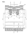
- FIG. 5 illustrates a schematic cross section through a cell structure of an IGBT power semiconductor component 5 including a vertical gate zone 7 arranged within a trench structure 8 of a power semiconductor chip 23 .
- the power semiconductor chip 23 has a semiconductor body 9 having a top side 31 and an underside 26 .
- the semiconductor body 9 has a field stop zone 24 and a lightly doped semiconductor layer 21 , in which a drift path 22 is arranged.
- the gate zone 7 projects into the drift path 22 and has a gate oxide 11 and a gate electrode 10 identified by G, wherein the gate oxide 11 is arranged on the trench walls 12 of the trench structure 8 .
- a p-conducting body zone 13 is arranged between two gate zones 7 , and is electrically connected to a metallic emitter electrode E via a highly doped p + -conducting region 28 .
- the body zone 13 is adjoined vertically by an n ⁇ -conducting drift zone 14 leading from an n ⁇ n junction with an n-conducting field stop zone 24 , which acts as a field stop junction 29 , to a further pn junction 25 of a p-conducting layer 30 on the underside of the semiconductor body 9 , which constitutes a rear side emitter ER, wherein a collector electrode C of the IGBT is arranged on the underside 26 of the semiconductor body 9 .
- the correspondingly weakly doped n-conducting field stop region of the substrate can dynamically supply an additional current during turn-off and thus decelerate the rise in the reverse voltage across the component.
- this capability depends greatly on the intermediate circuit voltage currently present, and therefore does not have a sufficiently large production window since the leakage current or the static reverse voltage likewise suffers from the lightly doped field stop region.
- the cell structure including emitter region, body zone, gate zone and drift path, in the region near the surface of the semiconductor body 9 is surrounded by a floating p-doped shielding zone 15 , wherein the shielding zone 15 extends into the semiconductor body 9 deeper than the trench gate structure.
- FIG. 6 illustrates an alternative solution for improving the power semiconductor component characteristic in which the trench structure 8 projects into the semiconductor body by its bottom region 17 deeper than the shielding zones 15 .
- this power semiconductor component 6 of the IGBT type a robust turn-off behavior is achieved by virtue of the fact that the trench bottom 17 is no longer covered by the floating p-doped shielding zones 15 .
- FIG. 1 illustrates a schematic cross section through a cell of a power semiconductor chip of a power semiconductor component 1 of a first embodiment of the invention.
- FIG. 2 illustrates a schematic cross section through a cell of a power semiconductor chip of a power semiconductor component 2 of a second embodiment of the invention.
- FIG. 3 illustrates a schematic cross section through a cell of a power semiconductor chip of a power semiconductor component 3 of a third embodiment of the invention.
- FIG. 4 illustrates a schematic cross section through a cell of a power semiconductor chip of a power semiconductor component 4 of a fourth embodiment of the invention.
- FIG. 5 illustrates a schematic cross section through a cell of a power semiconductor chip of a power semiconductor component 5 in accordance with a first version in the prior art.
- FIG. 6 illustrates a schematic cross section through a cell of a power semiconductor component 6 of a further version in the prior art.
- the hitherto known dimensioning of power semiconductor components leads to increased switching losses and thus to a reduced usability of, for example, IGBT switches and is associated with a considerable outlay in terms of costs and development for the customer, both for driving and for the power section.
- Embodiments of the invention overcome the disadvantages in the prior art and in this case take account of the respective loading by leakage inductances during component development.
- the aim is to configure the dynamic response of the turn-off behavior such that at customary values of the leakage inductance and the highest rated current in a housing, impermissibly high overvoltages still do not occur.
- a power semiconductor component includes vertical gate zones, wherein the gate zones are arranged in a trench structure of a semiconductor body.
- the gate zones for their part, have gate electrodes and a gate oxide, which covers the walls of the trench structure.
- a body zone of a first conduction type is arranged between two gate zones, the body zone being adjoined vertically by a drift zone of a complimentary conduction type with respect to the first conduction type.
- Shielding zones of the first conduction type are arranged adjacent to the gate zones, the shielding zones extending into the semiconductor body deeper than the trench structure of the gate zones and having a pn junction with the drift zone below the trench structure.
- This power semiconductor component has the following advantages.
- a buried dopant zone of the same charge type as the drift zone is arranged in the space charge region of the pn junction between drift zone and shielding zone at a distance from the trench bottom of the trench structure, and has a higher impurity concentration than the drift zone. Consequently, with this cell structure a dynamic avalanche effect is likewise achieved in the turn-off of the power semiconductor component for active voltage limiting in the cell array.
- the blocking capability of the edge of the power semiconductor component is not reduced further; furthermore, the load current or the avalanche current during turn-off is distributed between a large buried silicon area uniformly below the trench structure and a significantly improved switching robustness of the power semiconductor component is thus ensured, but at the same time hot charge carriers are no longer injected into the oxide in the bottom region of the trench structure by avalanche multiplication. Rather, the avalanche breakdown takes place at the more highly doped n-conducting dopant zones arranged in buried fashion below the trench bottom.
- a distance a between the n-conducting dopant zone and the bottom region of the trench structure of from 100 nanometers up to a few 100 nanometers is already sufficient, between 100 nm ⁇ a ⁇ 500 nm.
- Such a distance can be achieved by an implantation of an additional n-type doping into the trench bottoms with sufficiently high energy since the Bragg deceleration zone for implanted ions, in which a maximum of impurities is incorporated depending on the mass of the dopant in the semiconductor body below the trench bottom, is energy-dependent.
- the avalanche breakdown does not take place directly at the boundary between semiconductor material and oxide material of the gate structure, but instead centrally in the semiconductor material. It is therefore not possible for any hot charge carriers to be injected into the oxide of the walls of the trench structure, which charge carriers would lead to trapping in the oxide and hence to drift phenomena.
- Arsenic atoms are used for these n-type dopant cells since they outdiffuse to a significantly lesser extent than phosphorus atoms, for example, during the subsequent thermal processes.
- phosphorus is also suitable and has the advantage that it is lighter and can therefore be implanted into the semiconductor body deeper below the trench structure. In this case, the dose of the implanted n-type doping at the trench bottom is lower than the breakdown charge.
- the p-type doping of the shielding zones that is to be compensated for can be taken into account, of course, in the implanted dose of n-conducting impurity material.
- another p-type doping can additionally be implanted with low energy at the trench bottoms, which doping additionally shields the oxide against loading and the high hole current density that flows.
- the trench structure has a trench bottom which is covered with gate oxide and to which the shielding zone extends into the semiconductor body, wherein the gate oxide in the bottom region of the trench structure is adjoined by a conductive dopant zone within the shielding zone having an increased impurity concentration of the first conduction type, which also prevails in the shielding zone.
- a further variant which provides an additional n-type doping in the region of the trench is aimed at increasing the turn-on speed and thus at reducing the turn-on losses.
- the drift zone is to be flooded with charge carriers first before the voltage assumes very low values. The turn-on losses of shrunk IGBTs of this type cannot be reduced simply. Therefore, in this further embodiment of the invention, this additional n-type dopant zone is introduced at the trench bottom, as will be explained later with the aid of FIG.
- the dopant zone is either completely surrounded by shielding zones, as illustrated in FIG. 3 , or has a contact with the n ⁇ -conducting drift zone in the direction of the p-conducting body zone, such that the complimentarily conductive second dopant zone below the trench bottom projects laterally from the shielding zone right into the drift zone.
- This embodiment of the invention has the advantage that during turn-on a channel is formed between n + -type emitter and the additional n-conducting dopant zone at the trench bottom.
- the n-type dopant zone is virtually at emitter potential, while the floating p-doped shielding zone is at a higher potential.
- Electrons are injected from the n-conducting dopant zone into the shielding zone and thus analogously to the effect of an npn transistor into the n ⁇ -conducting drift zone. Electrons can therefore also be injected into the drift zone below the trench structure and be conveyed to the rear side emitter, which thereby injects holes more uniformly and thus floods the IGBT more rapidly.
- the buried n-doped dopant zone which enables dynamic limiting of the reverse voltage of the component, can additionally be provided, as illustrated in FIGS. 3 and 4 .
- the semiconductor body of the power semiconductor component is a silicon single crystal and the gate dielectric includes a thermal silicon oxide.
- This has the advantage that the silicon oxide can be produced technologically in highly pure form on the trench walls of a monocrystalline silicon body.
- the complementarily conductive dopant zones below the trench bottom have arsenic atoms at substitutional silicon lattice sites. Since arsenic atoms have a lower diffusion coefficient in the silicon lattice than phosphorus, they are maintained in the dopant zone once the latter has been doped, relatively unchanged during the subsequent high-temperature processes. In this case, it is advantageous that it is possible to comply with keeping the net impurity doping of the arsenic atoms in the dopant zone at a distance from the trench bottom lower than the breakdown charge.
- the gate electrode does not have any metal, but rather a highly doped, polycrystalline silicon. This has the advantage that it likewise retains its position during subsequent high-temperature processes and does not diffuse into the gate oxide or form recombination centers in the gate oxide in the form of traps.
- the power semiconductor component is an IGBT switch and is used for converter modules having rated voltages of typically 500 V to 6500 V.
- a method for producing a plurality of power semiconductor components including dopant zones, at a distance from a vertical trench structure including gate zones has the following method processes.
- the first process involves producing a semiconductor wafer with a multiplicity of semiconductor chip positions which are arranged in rows and columns and in which are arranged drift paths having a complimentary conduction type with respect to body zones and shielding zones having the same conduction type as the body zones.
- Construction of the trench structure can be followed by an ion implantation—masked as required—of dopants through the trench bottom of the trench structure for dopant zones that are at a distance from the trench bottom and have a complementary conduction type with respect to the shielding zones in the region of the pn junction between drift zones and shielding zones.
- the power semiconductor component structure is then completed in the semiconductor chip positions, and finally again the semiconductor wafer is separated into individual power semiconductor chips. Finally, the power semiconductor chips are subjected to packaging and external contact formation to form individual power semiconductor components.
- This method has the advantage that intermediate stages, such as the introduction of a trench structure, which is necessary for a power semiconductor component including a vertical trench zone, can be used in order to produce the additional buried dopant zones according to the invention below the trench bottom by using ion implantation without additional photoresist masks being required. It is advantageous, moreover, if the edge region of the respective semiconductor chip positions on the semiconductor wafer is protected against penetration of the impurities that are required for the dopant zones, in order that the dielectric strength of the edge zones is not decreased from the outset.
- arsenic ions are implanted through the trench bottom into the semiconductor body.
- a first dopant zone can be introduced into the semiconductor body at a distance from the trench bottom and a second dopant zone can be arranged directly at the trench bottom by using lower ion implantation energy.
- the state of the semiconductor wafer with a prepared trench structure can be used in order to introduce these two dopant zones using two implantation processes. If the dopant zone in direct proximity to the trench bottom is intended to have the doping of the shielding zones, then boron is implanted. If, by contrast, the dopant zone at the trench bottom is intended to correspond to the dopant of the drift zones, then arsenic is implanted and phosphorus is possibly used for a second and thus deeper dopant zone. In this case, in one implementation of the method, the same implantation energy can be used for both dopants, especially as phosphorus penetrates into the crystal deeper than arsenic on account of the smaller atomic mass.
- the n-type implantation after the shielding zone diffusion and after a thermal oxidation process, in which case the sacrificial oxide grown may simultaneously serve as a screen oxide.
- the implantation is then followed by the sacrificial oxide etch and the cell process for completing the IGBT structure.
- the dose of the n-type implantation is so low that no adverse effects are to be expected in the region of the cell and the shielding zones outside the trench bottoms since this dose is readily overcompensated for. It is advantageous, however, if the edge of the semiconductor chip positions is also provided with the trench mask and protected in order that no n-type implantation into the edge structure of the semiconductor chips takes place.
- an additional photolithography process may also be required, such that it is expedient to shield the outermost series of cells adjoining the edge from the n-type implantation for the dopant zones in order to protect this region against the additional avalanche loading.
- the discharging hole current densities are particularly high during turn-off, which would likewise lead to an earlier commencement of the dynamic avalanche and should therefore be avoided by protecting the edges.
- a monocrystalline silicon wafer in order to produce a semiconductor wafer having semiconductor chips arranged in rows and columns, firstly a monocrystalline silicon wafer is provided.
- the silicon wafer has the dopant concentration of the drift zones. However, it has a multiple thickness of the drift zones and is therefore thinned by grinding virtually to the thickness of the drift zones after completion of the semiconductor chip structures on the top side of the semiconductor wafer.
- a dopant concentration that is at least one power of ten higher than the drift zone doping is introduced into the semiconductor body from the rear side that has been thinned by grinding, in order to form an ohmic emitter rear side contact.
- An alternative possibility for producing a semiconductor wafer having semiconductor chips arranged in rows and columns consists in providing a monocrystalline semiconductor wafer which is doped more highly by at least one power of ten than the drift zones to be formed.
- An epitaxial layer having the dopant concentration of the drift zones and at least the thickness of the drift zones is deposited on the semiconductor wafer.
- the trench structure for the gate electrodes can then be worked into the epitaxial layer.
- FIG. 1 illustrates a schematic cross section through a cell of a power semiconductor chip 23 of a power semiconductor component 1 of a first embodiment of the invention.
- the construction of the cell corresponds in terms of construction to the cell in accordance with the prior art such as is illustrated by FIG. 5 .
- Component parts having the same functions as in FIG. 5 are identified by the same reference symbols in FIGS. 1 to 4 and are not discussed separately.
- a dopant zone 18 is arranged within the space charge zone of the pn junction 16 between the shielding zone 15 and the drift zone 14 below the vertical trench structure 8 including gate zones 7 , and there in particular below the trench bottom 17 , the dopant zone being n-conducting and having a higher impurity doping than the n ⁇ -conducting drift path 14 .
- avalanche breakdowns are brought about in the case of overvoltage and they enable a safeguarded switch-over to the off-state case and simultaneously keep the switch-over losses low.
- the avalanche breakdowns are arranged remote from the trench structure in the region of the dopant zone 18 introduced in buried fashion, such that no hot charge carriers can be injected into the oxide 11 of the trench structure 8 and the oxide 11 of the trench structure 8 is thus protected. A distance a of a few 100 nanometers from the trench bottom 17 already suffices for this purpose.
- FIG. 2 illustrates a schematic cross section through a cell of a power semiconductor chip 23 of a power semiconductor component 2 of a second embodiment of the invention.
- an additional second dopant zone 19 is arranged in the region of the trench bottom 17 by using ion implantation, in which case, in this second embodiment of the invention, the same conduction type as prevails in the shielding zone 15 is implanted.
- This p-conducting dopant zone 19 additionally protects the oxide 11 of the trench structure 8 and shields it from the penetration of hot electrons.
- FIG. 3 illustrates a schematic cross section through a cell of a power semiconductor chip 23 of a power semiconductor component 3 of a third embodiment of the invention.
- a dopant zone 20 was introduced in the region of the bottom 17 of the trench structure 8 , the dopant zone having the same conduction type as the drift zone 14 .
- a buried n-conducting dopant zone 18 is arranged at a distance from the trench bottom 17 in the semiconductor body 9 , and serves for reducing voltage spikes during switch-over through avalanche effects.
- the additional n-type doping at the trench bottom of the dopant zone 17 has the effect that a channel is formed between the n + -type emitter region and the additional n-type doping at the trench bottom.
- the n-type doping of the dopant zone is virtually at emitter potential, while the shielding zone 15 is at a higher potential.
- Electrons are injected from the n-type dopant zone 18 into the shielding zone 15 and into the n ⁇ -type drift zone 14 analogously to a mode of operation of an npn transistor. Consequently, electrons can be injected into the drift zone 14 below the trench structure 8 , and be conveyed to the rear side emitter ER, which thereby injects holes more uniformly and thus floods the IGBT more rapidly.
- FIG. 4 illustrates a schematic cross section through a cell of a power semiconductor chip 23 of a power semiconductor component 4 of a fourth embodiment of the invention.
- the difference between the fourth embodiment of the invention and the third embodiment of the invention is that the n-conducting dopant zone 20 in the region of the trench bottom 17 projects laterally from the shielding zone 15 into the drift path 14 .
- FIGS. 5 and 6 illustrate embodiments which are known from the prior art. FIGS. 4 and 5 will not be discussed again in order to avoid repetition.
- the semiconductor components are typically packaged in power semiconductor modules and used for converter applications.
Landscapes
- Electrodes Of Semiconductors (AREA)
Abstract
Description
Claims (20)
Applications Claiming Priority (3)
| Application Number | Priority Date | Filing Date | Title |
|---|---|---|---|
| DE102006024504 | 2006-05-23 | ||
| DE102006024504.0 | 2006-05-23 | ||
| DE102006024504A DE102006024504B4 (en) | 2006-05-23 | 2006-05-23 | Power semiconductor device with vertical gate zone and method for producing the same |
Publications (2)
| Publication Number | Publication Date |
|---|---|
| US20070272978A1 US20070272978A1 (en) | 2007-11-29 |
| US8044458B2 true US8044458B2 (en) | 2011-10-25 |
Family
ID=38622203
Family Applications (1)
| Application Number | Title | Priority Date | Filing Date |
|---|---|---|---|
| US11/752,590 Expired - Fee Related US8044458B2 (en) | 2006-05-23 | 2007-05-23 | Semiconductor device including a vertical gate zone, and method for producing the same |
Country Status (2)
| Country | Link |
|---|---|
| US (1) | US8044458B2 (en) |
| DE (1) | DE102006024504B4 (en) |
Cited By (2)
| Publication number | Priority date | Publication date | Assignee | Title |
|---|---|---|---|---|
| KR101376892B1 (en) | 2012-10-29 | 2014-03-20 | 삼성전기주식회사 | Semiconductor device |
| CN107527950A (en) * | 2016-06-21 | 2017-12-29 | 奥特润株式会社 | Power semiconductor arrangement and its manufacture method |
Families Citing this family (25)
| Publication number | Priority date | Publication date | Assignee | Title |
|---|---|---|---|---|
| US7875951B2 (en) * | 2007-12-12 | 2011-01-25 | Infineon Technologies Austria Ag | Semiconductor with active component and method for manufacture |
| US8264033B2 (en) * | 2009-07-21 | 2012-09-11 | Infineon Technologies Austria Ag | Semiconductor device having a floating semiconductor zone |
| CN102088031B (en) * | 2009-12-03 | 2013-04-17 | 无锡华润上华半导体有限公司 | N-type laterally diffused metal oxide semiconductor (NLDMOS) device and manufacturing method thereof |
| US8264035B2 (en) * | 2010-03-26 | 2012-09-11 | Force Mos Technology Co., Ltd. | Avalanche capability improvement in power semiconductor devices |
| US8441046B2 (en) * | 2010-10-31 | 2013-05-14 | Alpha And Omega Semiconductor Incorporated | Topside structures for an insulated gate bipolar transistor (IGBT) device to achieve improved device performances |
| US9105682B2 (en) | 2011-02-28 | 2015-08-11 | Infineon Technologies Austria Ag | Semiconductor component with improved dynamic behavior |
| CN103875076B (en) | 2011-11-28 | 2017-09-01 | 富士电机株式会社 | Insulated gate semiconductor device and its manufacture method |
| US10249721B2 (en) | 2013-04-04 | 2019-04-02 | Infineon Technologies Austria Ag | Semiconductor device including a gate trench and a source trench |
| US9666663B2 (en) | 2013-08-09 | 2017-05-30 | Infineon Technologies Ag | Semiconductor device with cell trench structures and contacts and method of manufacturing a semiconductor device |
| US9076838B2 (en) | 2013-09-13 | 2015-07-07 | Infineon Technologies Ag | Insulated gate bipolar transistor with mesa sections between cell trench structures and method of manufacturing |
| US9147763B2 (en) * | 2013-09-23 | 2015-09-29 | Infineon Technologies Austria Ag | Charge-compensation semiconductor device |
| US9123770B2 (en) | 2013-11-18 | 2015-09-01 | Alpha And Omega Semiconductor Incorporated | Charge reservoir IGBT top structure |
| US9105679B2 (en) | 2013-11-27 | 2015-08-11 | Infineon Technologies Ag | Semiconductor device and insulated gate bipolar transistor with barrier regions |
| US9385228B2 (en) | 2013-11-27 | 2016-07-05 | Infineon Technologies Ag | Semiconductor device with cell trench structures and contacts and method of manufacturing a semiconductor device |
| US9553179B2 (en) * | 2014-01-31 | 2017-01-24 | Infineon Technologies Ag | Semiconductor device and insulated gate bipolar transistor with barrier structure |
| US9318587B2 (en) | 2014-05-30 | 2016-04-19 | Alpha And Omega Semiconductor Incorporated | Injection control in semiconductor power devices |
| TWI559531B (en) * | 2014-08-20 | 2016-11-21 | 新唐科技股份有限公司 | Insulated gate bipolar transistor and method of manufacturing the same |
| JP6471508B2 (en) * | 2015-01-19 | 2019-02-20 | 富士電機株式会社 | Semiconductor device |
| US10930774B2 (en) * | 2019-07-16 | 2021-02-23 | Nami MOS CO., LTD. | Shielded gate trench MOSFETs with floating trenched gates and channel stop trenched gates in termination |
| DE102019212641A1 (en) * | 2019-08-23 | 2021-02-25 | Robert Bosch Gmbh | VERTICAL FIELD EFFECT TRANSISTOR AND METHOD OF TRAINING THE SAME |
| CN112117327B (en) * | 2020-08-17 | 2022-06-28 | 江苏东海半导体科技有限公司 | IGBT device and manufacturing process thereof |
| CN112802749A (en) * | 2021-01-06 | 2021-05-14 | 江苏东海半导体科技有限公司 | Trench IGBT structure polycrystalline silicon morphology optimization process |
| CN112928155B (en) * | 2021-04-01 | 2022-04-12 | 四川大学 | A trench-gate superjunction IGBT with floating p-pillar |
| CN113764511B (en) * | 2021-07-30 | 2023-10-27 | 广州华浦电子科技有限公司 | Low-loss superjunction IGBT device with dynamic carrier channel and manufacturing method thereof |
| CN115799306A (en) * | 2022-11-23 | 2023-03-14 | 电子科技大学 | A Novel IGBT Structure with Enhanced Gate Controllability |
Citations (13)
| Publication number | Priority date | Publication date | Assignee | Title |
|---|---|---|---|---|
| US4893160A (en) | 1987-11-13 | 1990-01-09 | Siliconix Incorporated | Method for increasing the performance of trenched devices and the resulting structure |
| US5304821A (en) * | 1990-10-08 | 1994-04-19 | Mitsubishi Denki Kabushiki Kaisha | MOS-gate-turnoff thyristor |
| US5629543A (en) * | 1995-08-21 | 1997-05-13 | Siliconix Incorporated | Trenched DMOS transistor with buried layer for reduced on-resistance and ruggedness |
| US5843796A (en) * | 1995-09-11 | 1998-12-01 | Delco Electronics Corporation | Method of making an insulated gate bipolar transistor with high-energy P+ im |
| US6091107A (en) * | 1997-01-21 | 2000-07-18 | Mitel Semiconductor Limited | Semiconductor devices |
| US6137122A (en) * | 1999-12-02 | 2000-10-24 | Analog And Power Electronics Corp. | Latch-up controllable insulated gate bipolar transistor |
| DE10005772A1 (en) | 2000-02-10 | 2001-08-23 | Infineon Technologies Ag | Trench MOSFET |
| WO2002019434A1 (en) | 2000-08-30 | 2002-03-07 | Infineon Technologies Ag | Trench igbt |
| US6380569B1 (en) * | 1999-08-10 | 2002-04-30 | Rockwell Science Center, Llc | High power unipolar FET switch |
| US20030201454A1 (en) * | 2002-04-25 | 2003-10-30 | International Rectifier Corp. | Trench IGBT |
| US6686612B1 (en) * | 2002-10-01 | 2004-02-03 | T-Ram, Inc. | Thyristor-based device adapted to inhibit parasitic current |
| US7199404B2 (en) * | 2003-12-25 | 2007-04-03 | Nec Electronics Corporation | Semiconductor substrate and semiconductor device using the same |
| US7625793B2 (en) * | 1999-12-20 | 2009-12-01 | Fairchild Semiconductor Corporation | Power MOS device with improved gate charge performance |
-
2006
- 2006-05-23 DE DE102006024504A patent/DE102006024504B4/en not_active Expired - Fee Related
-
2007
- 2007-05-23 US US11/752,590 patent/US8044458B2/en not_active Expired - Fee Related
Patent Citations (14)
| Publication number | Priority date | Publication date | Assignee | Title |
|---|---|---|---|---|
| US4893160A (en) | 1987-11-13 | 1990-01-09 | Siliconix Incorporated | Method for increasing the performance of trenched devices and the resulting structure |
| US5304821A (en) * | 1990-10-08 | 1994-04-19 | Mitsubishi Denki Kabushiki Kaisha | MOS-gate-turnoff thyristor |
| US5629543A (en) * | 1995-08-21 | 1997-05-13 | Siliconix Incorporated | Trenched DMOS transistor with buried layer for reduced on-resistance and ruggedness |
| US5843796A (en) * | 1995-09-11 | 1998-12-01 | Delco Electronics Corporation | Method of making an insulated gate bipolar transistor with high-energy P+ im |
| US6091107A (en) * | 1997-01-21 | 2000-07-18 | Mitel Semiconductor Limited | Semiconductor devices |
| US6380569B1 (en) * | 1999-08-10 | 2002-04-30 | Rockwell Science Center, Llc | High power unipolar FET switch |
| US6137122A (en) * | 1999-12-02 | 2000-10-24 | Analog And Power Electronics Corp. | Latch-up controllable insulated gate bipolar transistor |
| US7625793B2 (en) * | 1999-12-20 | 2009-12-01 | Fairchild Semiconductor Corporation | Power MOS device with improved gate charge performance |
| DE10005772A1 (en) | 2000-02-10 | 2001-08-23 | Infineon Technologies Ag | Trench MOSFET |
| DE10085054B4 (en) | 2000-08-30 | 2005-12-15 | Infineon Technologies Ag | Trench IGBT |
| WO2002019434A1 (en) | 2000-08-30 | 2002-03-07 | Infineon Technologies Ag | Trench igbt |
| US20030201454A1 (en) * | 2002-04-25 | 2003-10-30 | International Rectifier Corp. | Trench IGBT |
| US6686612B1 (en) * | 2002-10-01 | 2004-02-03 | T-Ram, Inc. | Thyristor-based device adapted to inhibit parasitic current |
| US7199404B2 (en) * | 2003-12-25 | 2007-04-03 | Nec Electronics Corporation | Semiconductor substrate and semiconductor device using the same |
Cited By (3)
| Publication number | Priority date | Publication date | Assignee | Title |
|---|---|---|---|---|
| KR101376892B1 (en) | 2012-10-29 | 2014-03-20 | 삼성전기주식회사 | Semiconductor device |
| CN107527950A (en) * | 2016-06-21 | 2017-12-29 | 奥特润株式会社 | Power semiconductor arrangement and its manufacture method |
| CN107527950B (en) * | 2016-06-21 | 2020-10-27 | 奥特润株式会社 | Power semiconductor device and method for manufacturing the same |
Also Published As
| Publication number | Publication date |
|---|---|
| DE102006024504A1 (en) | 2007-11-29 |
| US20070272978A1 (en) | 2007-11-29 |
| DE102006024504B4 (en) | 2010-09-02 |
Similar Documents
| Publication | Publication Date | Title |
|---|---|---|
| US8044458B2 (en) | Semiconductor device including a vertical gate zone, and method for producing the same | |
| US8592894B2 (en) | Method of forming a power semiconductor device and power semiconductor device | |
| US9064923B2 (en) | Bipolar semiconductor component with a fully depletable channel zone | |
| US9337185B2 (en) | Semiconductor devices | |
| US7915675B2 (en) | IGBT having one or more stacked zones formed within a second layer of the IGBT | |
| US9419080B2 (en) | Semiconductor device with recombination region | |
| US7932583B2 (en) | Reduced free-charge carrier lifetime device | |
| US10211057B2 (en) | Transistor component with reduced short-circuit current | |
| US20020179968A1 (en) | Power semiconductor component, compensation component, power transistor, and method for producing power semiconductor components | |
| CN113972271B (en) | Power semiconductor devices | |
| US10593789B2 (en) | Semiconductor apparatus and method of manufacturing the same | |
| JP7118033B2 (en) | semiconductor equipment | |
| JPH09139510A (en) | Semiconductor device and manufacturing method thereof | |
| US7569431B2 (en) | Semiconductor device and manufacturing method thereof | |
| JP7405261B2 (en) | semiconductor equipment | |
| US6147381A (en) | Field effect-controllable semiconductor component | |
| CN105957901B (en) | Semiconductor device with trench-Schottky-barrier-Schottky-diode | |
| US20220375811A1 (en) | Power Semiconductor Device | |
| JP4904635B2 (en) | Semiconductor device and manufacturing method thereof | |
| KR102924420B1 (en) | Igbt chip with improved switching speed and manufacturing method therefor | |
| US11757017B2 (en) | Anti-parallel diode formed using damaged crystal structure in a vertical power device |
Legal Events
| Date | Code | Title | Description |
|---|---|---|---|
| AS | Assignment |
Owner name: INFINEON TECHNOLOGIES AUSTRIA AG, AUSTRIA Free format text: ASSIGNMENT OF ASSIGNORS INTEREST;ASSIGNORS:MAUDER, ANTON;SCHULZE, HANS-JOACHIM;REEL/FRAME:019627/0888 Effective date: 20070713 |
|
| FEPP | Fee payment procedure |
Free format text: PAYOR NUMBER ASSIGNED (ORIGINAL EVENT CODE: ASPN); ENTITY STATUS OF PATENT OWNER: LARGE ENTITY |
|
| ZAAA | Notice of allowance and fees due |
Free format text: ORIGINAL CODE: NOA |
|
| ZAAB | Notice of allowance mailed |
Free format text: ORIGINAL CODE: MN/=. |
|
| STCF | Information on status: patent grant |
Free format text: PATENTED CASE |
|
| FPAY | Fee payment |
Year of fee payment: 4 |
|
| MAFP | Maintenance fee payment |
Free format text: PAYMENT OF MAINTENANCE FEE, 8TH YEAR, LARGE ENTITY (ORIGINAL EVENT CODE: M1552); ENTITY STATUS OF PATENT OWNER: LARGE ENTITY Year of fee payment: 8 |
|
| FEPP | Fee payment procedure |
Free format text: MAINTENANCE FEE REMINDER MAILED (ORIGINAL EVENT CODE: REM.); ENTITY STATUS OF PATENT OWNER: LARGE ENTITY |
|
| LAPS | Lapse for failure to pay maintenance fees |
Free format text: PATENT EXPIRED FOR FAILURE TO PAY MAINTENANCE FEES (ORIGINAL EVENT CODE: EXP.); ENTITY STATUS OF PATENT OWNER: LARGE ENTITY |
|
| STCH | Information on status: patent discontinuation |
Free format text: PATENT EXPIRED DUE TO NONPAYMENT OF MAINTENANCE FEES UNDER 37 CFR 1.362 |
|
| FP | Lapsed due to failure to pay maintenance fee |
Effective date: 20231025 |