US8031984B2 - Semiconductor optical modulator - Google Patents
Semiconductor optical modulator Download PDFInfo
- Publication number
- US8031984B2 US8031984B2 US12/445,616 US44561607A US8031984B2 US 8031984 B2 US8031984 B2 US 8031984B2 US 44561607 A US44561607 A US 44561607A US 8031984 B2 US8031984 B2 US 8031984B2
- Authority
- US
- United States
- Prior art keywords
- layer
- type
- optical modulator
- cladding layer
- type cladding
- Prior art date
- Legal status (The legal status is an assumption and is not a legal conclusion. Google has not performed a legal analysis and makes no representation as to the accuracy of the status listed.)
- Active, expires
Links
- 230000003287 optical effect Effects 0.000 title claims abstract description 79
- 239000004065 semiconductor Substances 0.000 title claims abstract description 52
- 239000010410 layer Substances 0.000 claims abstract description 160
- 238000005253 cladding Methods 0.000 claims abstract description 75
- 239000012792 core layer Substances 0.000 claims abstract description 25
- 239000000758 substrate Substances 0.000 claims abstract description 6
- 230000031700 light absorption Effects 0.000 abstract description 8
- 238000004519 manufacturing process Methods 0.000 abstract description 7
- 238000009825 accumulation Methods 0.000 abstract description 3
- 238000000034 method Methods 0.000 abstract description 2
- 230000004888 barrier function Effects 0.000 description 13
- 238000010586 diagram Methods 0.000 description 10
- 230000007423 decrease Effects 0.000 description 8
- 229910003327 LiNbO3 Inorganic materials 0.000 description 6
- 230000000694 effects Effects 0.000 description 5
- 125000005842 heteroatom Chemical group 0.000 description 5
- 239000000969 carrier Substances 0.000 description 4
- 230000008859 change Effects 0.000 description 4
- 229910001218 Gallium arsenide Inorganic materials 0.000 description 3
- 239000000463 material Substances 0.000 description 3
- 230000008901 benefit Effects 0.000 description 2
- 238000009792 diffusion process Methods 0.000 description 2
- 239000006185 dispersion Substances 0.000 description 2
- 238000005516 engineering process Methods 0.000 description 2
- 229910000530 Gallium indium arsenide Inorganic materials 0.000 description 1
- 229910045601 alloy Inorganic materials 0.000 description 1
- 239000000956 alloy Substances 0.000 description 1
- 229910001423 beryllium ion Inorganic materials 0.000 description 1
- 230000015572 biosynthetic process Effects 0.000 description 1
- 230000000903 blocking effect Effects 0.000 description 1
- 239000011248 coating agent Substances 0.000 description 1
- 238000000576 coating method Methods 0.000 description 1
- 238000004891 communication Methods 0.000 description 1
- 238000000151 deposition Methods 0.000 description 1
- 230000005684 electric field Effects 0.000 description 1
- 239000000835 fiber Substances 0.000 description 1
- 238000002513 implantation Methods 0.000 description 1
- 230000001939 inductive effect Effects 0.000 description 1
- 238000002347 injection Methods 0.000 description 1
- 239000007924 injection Substances 0.000 description 1
- 238000005468 ion implantation Methods 0.000 description 1
- 239000000203 mixture Substances 0.000 description 1
- 230000007935 neutral effect Effects 0.000 description 1
- 230000005693 optoelectronics Effects 0.000 description 1
- 230000001902 propagating effect Effects 0.000 description 1
- 238000005215 recombination Methods 0.000 description 1
- 230000006798 recombination Effects 0.000 description 1
- 230000009467 reduction Effects 0.000 description 1
- 230000004044 response Effects 0.000 description 1
- 238000010408 sweeping Methods 0.000 description 1
Images


Classifications
-
- G—PHYSICS
- G02—OPTICS
- G02F—OPTICAL DEVICES OR ARRANGEMENTS FOR THE CONTROL OF LIGHT BY MODIFICATION OF THE OPTICAL PROPERTIES OF THE MEDIA OF THE ELEMENTS INVOLVED THEREIN; NON-LINEAR OPTICS; FREQUENCY-CHANGING OF LIGHT; OPTICAL LOGIC ELEMENTS; OPTICAL ANALOGUE/DIGITAL CONVERTERS
- G02F1/00—Devices or arrangements for the control of the intensity, colour, phase, polarisation or direction of light arriving from an independent light source, e.g. switching, gating or modulating; Non-linear optics
- G02F1/01—Devices or arrangements for the control of the intensity, colour, phase, polarisation or direction of light arriving from an independent light source, e.g. switching, gating or modulating; Non-linear optics for the control of the intensity, phase, polarisation or colour
- G02F1/015—Devices or arrangements for the control of the intensity, colour, phase, polarisation or direction of light arriving from an independent light source, e.g. switching, gating or modulating; Non-linear optics for the control of the intensity, phase, polarisation or colour based on semiconductor elements having potential barriers, e.g. having a PN or PIN junction
- G02F1/017—Structures with periodic or quasi periodic potential variation, e.g. superlattices, quantum wells
-
- B—PERFORMING OPERATIONS; TRANSPORTING
- B82—NANOTECHNOLOGY
- B82Y—SPECIFIC USES OR APPLICATIONS OF NANOSTRUCTURES; MEASUREMENT OR ANALYSIS OF NANOSTRUCTURES; MANUFACTURE OR TREATMENT OF NANOSTRUCTURES
- B82Y20/00—Nanooptics, e.g. quantum optics or photonic crystals
-
- G—PHYSICS
- G02—OPTICS
- G02F—OPTICAL DEVICES OR ARRANGEMENTS FOR THE CONTROL OF LIGHT BY MODIFICATION OF THE OPTICAL PROPERTIES OF THE MEDIA OF THE ELEMENTS INVOLVED THEREIN; NON-LINEAR OPTICS; FREQUENCY-CHANGING OF LIGHT; OPTICAL LOGIC ELEMENTS; OPTICAL ANALOGUE/DIGITAL CONVERTERS
- G02F1/00—Devices or arrangements for the control of the intensity, colour, phase, polarisation or direction of light arriving from an independent light source, e.g. switching, gating or modulating; Non-linear optics
- G02F1/01—Devices or arrangements for the control of the intensity, colour, phase, polarisation or direction of light arriving from an independent light source, e.g. switching, gating or modulating; Non-linear optics for the control of the intensity, phase, polarisation or colour
- G02F1/015—Devices or arrangements for the control of the intensity, colour, phase, polarisation or direction of light arriving from an independent light source, e.g. switching, gating or modulating; Non-linear optics for the control of the intensity, phase, polarisation or colour based on semiconductor elements having potential barriers, e.g. having a PN or PIN junction
- G02F1/025—Devices or arrangements for the control of the intensity, colour, phase, polarisation or direction of light arriving from an independent light source, e.g. switching, gating or modulating; Non-linear optics for the control of the intensity, phase, polarisation or colour based on semiconductor elements having potential barriers, e.g. having a PN or PIN junction in an optical waveguide structure
-
- G—PHYSICS
- G02—OPTICS
- G02F—OPTICAL DEVICES OR ARRANGEMENTS FOR THE CONTROL OF LIGHT BY MODIFICATION OF THE OPTICAL PROPERTIES OF THE MEDIA OF THE ELEMENTS INVOLVED THEREIN; NON-LINEAR OPTICS; FREQUENCY-CHANGING OF LIGHT; OPTICAL LOGIC ELEMENTS; OPTICAL ANALOGUE/DIGITAL CONVERTERS
- G02F2202/00—Materials and properties
- G02F2202/10—Materials and properties semiconductor
- G02F2202/101—Ga×As and alloy
Definitions
- the present invention relates to a semiconductor optical modulator and, more particularly, to an ultra-high speed semiconductor optical modulator operating in a long wavelength region.
- Optical signals used in a long-distance wavelength multiplexed optical communication system are required to have small wavelength chirp in order to suppress the influence of the fiber dispersion effect.
- Such optical signals are usually generated by a configuration combined with a laser diode light source and an external modulator.
- a typical external modulator of this kind is an LN modulator fabricated with LiNbO3 (LN) waveguides.
- the operation principle of the LN modulator is to couple an optical waveguide with an electrical waveguide, inducing a change in refractive index based on the electro-optic effect by an electrical signal input and creating a phase change in the optical signal.
- Such LN modulator includes not only a simple optical phase modulator, but also an optical intensity modulator composed of a Mach-Zehnder interferometer, and a device operating as a highly-functional optical switch with numbers of waveguides combined, etc.
- a semiconductor optical modulator using the same principle of operation as the LN modulator there exists a semiconductor optical modulator using the same principle of operation as the LN modulator.
- a GaAs optical modulator in which a Schottky electrode is disposed on semi-insulating GaAs and formed as an opto-electronic waveguide, an InP/InGaAsP optical modulator configured to apply a voltage more effectively to the core portion of the waveguide along with the optical confinement by using a hetero pn-junction, and the like.
- semiconductor optical modulators have an advantage of a small size, there is a problem that the driving voltage is high in both the GaAs optical modulators and the pn-junction type InP/InGaAsP optical modulators.
- npin-type optical modulator structure in which both InP cladding layers are made n-type and a thin p layer (p-type barrier layer) is inserted between the two n layers as a barrier layer for suppressing an electron current (Patent Document 1).
- This npin-type allows the use of a relatively long waveguide because no p-type cladding layer having large optical loss is used.
- it has the degree of freedom in that the thickness of a depletion layer can be optimally designed at any value, a reduction of a driving voltage and matching between the electric speed and the light speed can easily be satisfied simultaneously, which is an advantage to improving the response speed of a modulator.
- the npin-type optical modulator has a semiconductor layer structure similar to that of a transistor, and therefore, when finite light absorption occurs, there is a problem that generated hole carriers accumulate in the p-type barrier layer. Due to this phenomenon, the height of barriers decreases which causes what is called the phototransistor behavior. This can cause not only an increase in the electron current across terminals, i.e., a decrease in withstand voltage, but also dispersion in frequency. Thus, what has been proposed is a structure for sweeping out the accumulated holes by locally forming a new p-type layer (Patent Document 2). However, it has a disadvantage in that it is structurally complex.
- FIG. 8 shows the structure of a semiconductor optical modulator according to such conventional technology.
- This semiconductor optical modulator 80 has first n-type electrode layer 82 - 1 formed on semiconductor substrate 81 , on which first n-type electrode 88 - 1 and first n-type cladding layer 83 - 1 are formed.
- first n-type cladding layer 83 - 1 layers are further stacked in order of first low-concentration cladding layer 85 - 1 , first intermediate layer 86 - 1 , core layer 87 , second intermediate layer 86 - 2 , second low-concentration cladding layer 85 - 2 , p-type cladding layer 84 , second n-type cladding layer 83 - 2 , second n-type electrode layer 82 - 2 , and second n-type electrode 88 - 2 .
- regions 89 are formed in which the conductive type is changed from n-type to p-type.
- the core layer 87 is configured such that the electro-optic effect works effectively at an operating optical wavelength.
- Second intermediate layer 86 - 2 serves as a connecting layer for preventing carriers occurred due to light absorption from being trapped at a hetero interface, and p-type cladding layer 84 serves as an electronic barrier.
- second n-type electrode 88 - 2 is in contact with second n-type electrode layer 82 - 2 and p-type regions 89 , and has the same electric potential.
- the present invention has been made in view of such problems, and the object of the invention is to provide an npin-type optical modulator that has a high reverse voltage and is simple to fabricate.
- a semiconductor optical modulator is an npin-type semiconductor optical modulator having layers stacked with a cathode layer arranged on the substrate side, including at least a first n-type cladding layer, a p-type cladding layer, a core layer and a second n-type cladding layer, which is characterized in that the p-type cladding layer is electrically connected to an electrode of the cathode layer.
- the semiconductor optical modulator according to an embodiment of the present invention is characterized in that the p-type cladding layer forms a mesa and a side surface of the mesa is electrically connected to the electrode of the cathode layer.
- the semiconductor optical modulator according to an embodiment of the present invention is characterized in that a p-type ohmic region is formed in a portion of the p-type cladding layer and the p-type ohmic region is electrically connected to the electrode of the cathode layer.
- the semiconductor optical modulator according to an embodiment of the present invention is characterized in that it includes a first intermediate layer below the core layer and a second intermediate layer above the core layer, wherein the band gap energy of the first intermediate layer is larger than that of the core layer and is smaller than that of a layer below the first intermediate layer, and wherein the band gap energy of the second intermediate layer is larger than that of the core layer and is smaller than that of a layer above the second intermediate layer.
- the semiconductor optical modulator according to an embodiment of the present invention is characterized in that the p-type cladding layer has a smaller electron affinity than that of the first n-type cladding layer.
- FIG. 1 is a sectional view of a semiconductor optical modulator in accordance with the first embodiment of the present invention
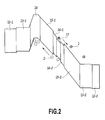
- FIG. 2 is a band diagram in a section along the line segment II-II′ of FIG. 1 ;
- FIG. 3 is a band diagram in a section along the line segment III-III′ of FIG. 1 ;
- FIG. 4 is a sectional view of a semiconductor optical modulator in accordance with the second embodiment of the present invention.
- FIG. 5 is a sectional view of a semiconductor optical modulator in accordance with the third embodiment of the present invention.
- FIG. 6 is a band diagram in a section along the line segment VI-VI′ of FIG. 5 ;
- FIG. 7 is a band diagram of a semiconductor optical modulator in an embodiment in accordance with the fourth embodiment of the present invention.
- FIG. 8 is a diagram showing an example of the structure of a semiconductor optical modulator according to a conventional technology.
- FIG. 1 shows a sectional view of a semiconductor optical modulator in accordance with the first embodiment of the present invention.
- first n-type electrode layer (n+-InP) 12 - 1 is formed on semi-insulating InP substrate 11 , and on top of that, first n-type cladding layer (n-Inp) 13 - 1 is formed.
- p-InP p-type cladding layer
- p-InP p-type electrode 19 and first low-concentration cladding layer (ud-InP) 15 - 1 are formed.
- first n-type electrode 18 - 1 in contact with first n-type electrode layer 12 - 1 is formed on top of the p-type electrode 19 .
- first low-concentration cladding layer 15 - 1 layers are further stacked in order of first intermediate layer (ud-InGaAsP) 16 - 1 , core layer 17 , second intermediate layer (ud-InGaAsP) 16 - 2 , second low-concentration cladding layer (usually, n ⁇ -InP) 15 - 2 , second n-type cladding layer (n-InP) 13 - 2 , second n-type electrode layer (n+-InP) 12 - 2 , and second n-type electrode 18 - 2 .
- Core layer 17 is structured such that the electro-optic effect works effectively at an operating optical wavelength.
- a multi-quantum-well structure may be employed making InGaAs layers with the Ga/Al composition varied as quantum well layers and quantum barrier layers.
- the first intermediate layer 16 - 1 serves as a connecting layer for preventing carriers generated due to light absorption from being trapped at a hetero interface.
- first n-type electrode layer 12 - 1 to second n-type electrode layer 12 - 2 are epitaxially grown and then the layers from first low-concentration cladding layer 15 - 1 to second n-type electrode layer 12 - 2 are etched to form a mesa type waveguide structure.
- first n-type cladding layer 13 - 1 and p-type cladding layer 14 are etched to expose first n-type electrode layer 12 - 1 .
- p-type electrode 19 , first n-type electrode 18 - 1 and second n-type electrode 18 - 2 are formed, respectively.
- the mesa surface may be protected by depositing a passivative coating.
- FIGS. 2 and 3 are band diagram in a section along the line segment II-II′ of FIG. 1 and FIG. 3 is a band diagram in a section along the line segment of FIG. 1 .
- p-type cladding layer 14 is neutralized or depleted, a barrier against electrons is formed, thereby suppressing the electron injection from n-type cladding layer 13 - 1 .
- the optical waveguide is formed with the layers from 13 - 1 to 13 - 2 , and the light propagating in this waveguide is modulated by a change in refractive index that occurs due to voltage application.
- the optical waveguide is formed with the layers from 13 - 1 to 13 - 2 , and the light propagating in this waveguide is modulated by a change in refractive index that occurs due to voltage application.
- the optical waveguide is formed with the layers from 13 - 1 to 13 - 2 , and the light propagating in this waveguide is modulated by a change in refractive index that occurs due to voltage application.
- holes 2 are trapped in p-type cladding layer 14 .
- semiconductor optical modulator 10 because p-type cladding layer 14 is connected to first n-type electrode 18 - 1 via p-type electrode 19 , even when a neutral layer does not remain in p-type cladding layer 14 immediately under p-type electrode 19 , excessive holes flow laterally in p-type cladding layer 14 ( FIG. 1 ) and are eventually absorbed in p-type electrode 19 beyond a Schottky barrier formed at the interface of the P-type cladding layer/p-type electrode interface ( FIG. 3 ). Then, by connecting p-type electrode 19 in contact with p-type cladding layer 14 to n-type electrode 18 - 1 , the problem of accumulation of holes that occurs in an optical modulator of this kind can comparatively easily be resolved.
- FIG. 4 shows a sectional view of a semiconductor optical modulator in accordance with the second embodiment of the present invention.
- This semiconductor optical modulator 20 in accordance with the second embodiment of the present invention works essentially in the same way as the semiconductor optical modulator 10 in accordance with the first embodiment.
- p-type electrode 19 is formed on the side surface of the mesa composed of first n-type cladding layer 13 - 1 , p-type cladding layer 14 , and first low-concentration cladding layer 15 - 1 .
- p-type cladding layer 14 In p-type cladding layer 14 , when the doping concentration is set low, this layer becomes more depleted due to the surface charge. Therefore, the electric potential in a depleted portion increases, the conductivity of this p-type cladding layer decreases, and the lateral flow of holes 2 may become insufficient. In a structure in which the top of p-type cladding layer 14 is covered with first low-concentration cladding layer 15 - 1 , as shown in FIG. 4 , as the influence of the surface charge decreases and the above-described blocking factor decreases, the p-type cladding layer can readily exhibit its inherent effect.
- FIG. 5 shows a sectional view of a semiconductor optical modulator in accordance with the third embodiment of the present invention.
- p-type ohmic region 4 is formed on the side surface of the mesa composed of first low-concentration cladding layer 15 - 1 , p-type cladding layer 14 , and first n-type cladding layer 13 - 1 .
- This p-type ohmic region 4 can be formed by thermally diffusing Zn after the formation of the mesa or by diffusing Zn when forming p-type electrode 19 composed of an alloy layer with Au and Zn.
- FIG. 6 shows a band diagram in a section along the line segment VI-VI′ of FIG. 5 . Because p-type ohmic region 4 has a higher doping concentration than p-type cladding layer 14 , as shown in FIG. 6 , a tunnel barrier against holes becomes thin, and it, therefore, does not prevent the flow of holes and can more effectively eliminate holes 2 by p-type electrode 19 .
- a semiconductor optical modulator in accordance with the fourth embodiment of the present invention has a hetero junction structure in which p-type cladding layer 14 in the structures of the above-described first to third embodiments is replaced with a semiconductor material having a smaller electron affinity than first n-type cladding layer 13 - 1 , typically, with InAlAs.
- This is a kind of what is called type II hetero junction.
- the band diagram in this structure is shown in FIG. 7 . Because the electric potential of this replaced portion 14 ′ becomes relatively low, a structure having a higher barrier against electrons will result. With this structure, the barrier against the accumulated hole charges becomes higher and it can keep back a decrease in withstand voltage associated with the phototransistor behavior.
- the semiconductor optical modulators in accordance with the present invention can solve the problem “the decrease in applicable reverse voltage” which is caused by a phenomenon “the accumulation of holes associated with light absorption” in npin-type optical modulators having the feature of low driving voltage. Furthermore, it is not required to change the conductive type in portions of the regions by Zn diffusion and Be ion implantation as seen in Patent Document 2, which makes manufacturing process relatively simple and does not incur an increase in the manufacturing cost. Accordingly, optical modulators with higher reverse voltage and more stability can be manufactured at low cost.
- the present invention has been described specifically based on several embodiments, in view of many feasible forms to which the principle of the invention can be applied, the embodiments described herein are illustrative only and are not intended to limit the scope of the invention.
- the single waveguide structure serving as an optical modulator is described.
- a Mach-Zehnder type optical modulator, an optical cross-connect switch and the like may be configured.
- InP and InGaAsP are used as semiconductor materials, other structures are also feasible such as a structure with InGaAsP replaced with InGaAlAs and a structure with InGaAsP and InGaAlAs combined, the above embodiments are not to limit semiconductor materials.
- the structure and details of the embodiments described herein can be modified without departing from the spirit of the present invention.
Landscapes
- Physics & Mathematics (AREA)
- Nonlinear Science (AREA)
- Optics & Photonics (AREA)
- General Physics & Mathematics (AREA)
- Chemical & Material Sciences (AREA)
- Engineering & Computer Science (AREA)
- Nanotechnology (AREA)
- Life Sciences & Earth Sciences (AREA)
- Biophysics (AREA)
- Crystallography & Structural Chemistry (AREA)
- Optical Modulation, Optical Deflection, Nonlinear Optics, Optical Demodulation, Optical Logic Elements (AREA)
- Semiconductor Lasers (AREA)
Abstract
Description
- Japanese Patent Laid-Open No. 2005-099387
- Japanese Patent Laid-Open No. 2005-114868 (FIGS. 1 to 3)
Claims (11)
Applications Claiming Priority (3)
| Application Number | Priority Date | Filing Date | Title |
|---|---|---|---|
| JP2006288839A JP4870518B2 (en) | 2006-10-24 | 2006-10-24 | Semiconductor optical modulator |
| JP2006-288839 | 2006-10-24 | ||
| PCT/JP2007/070752 WO2008050809A1 (en) | 2006-10-24 | 2007-10-24 | Semiconductor optical modulator |
Publications (2)
| Publication Number | Publication Date |
|---|---|
| US20100296766A1 US20100296766A1 (en) | 2010-11-25 |
| US8031984B2 true US8031984B2 (en) | 2011-10-04 |
Family
ID=39324603
Family Applications (1)
| Application Number | Title | Priority Date | Filing Date |
|---|---|---|---|
| US12/445,616 Active 2028-10-25 US8031984B2 (en) | 2006-10-24 | 2007-10-24 | Semiconductor optical modulator |
Country Status (8)
| Country | Link |
|---|---|
| US (1) | US8031984B2 (en) |
| EP (1) | EP2081075B1 (en) |
| JP (1) | JP4870518B2 (en) |
| KR (1) | KR101045758B1 (en) |
| CN (1) | CN101529313B (en) |
| AT (1) | ATE504027T1 (en) |
| DE (1) | DE602007013595D1 (en) |
| WO (1) | WO2008050809A1 (en) |
Cited By (1)
| Publication number | Priority date | Publication date | Assignee | Title |
|---|---|---|---|---|
| WO2022233396A1 (en) | 2021-05-04 | 2022-11-10 | Huawei Technologies Co., Ltd. | High speed membrane electro-optic modulator apparatus and method of manufacture |
Families Citing this family (11)
| Publication number | Priority date | Publication date | Assignee | Title |
|---|---|---|---|---|
| JP4870518B2 (en) * | 2006-10-24 | 2012-02-08 | Nttエレクトロニクス株式会社 | Semiconductor optical modulator |
| US9151592B2 (en) | 2012-01-03 | 2015-10-06 | Skorpios Technologies, Inc. | Method and system for multiple resonance interferometer |
| WO2013155378A1 (en) * | 2012-04-13 | 2013-10-17 | Skorpios Technologies, Inc. | Hybrid optical modulator |
| WO2016078057A1 (en) * | 2014-11-20 | 2016-05-26 | 华为技术有限公司 | InP-BASED MODULATOR |
| KR102163885B1 (en) * | 2015-01-14 | 2020-10-13 | 한국전자통신연구원 | Electro-absorption optical modulation device and the method of fabricating the same |
| CA2988051C (en) | 2015-06-02 | 2020-02-18 | Nippon Telegraph And Telephone Corporation | Semiconductor optical modulation element |
| JP2017167359A (en) * | 2016-03-16 | 2017-09-21 | 日本電信電話株式会社 | Ridge-waveguide optical modulator |
| EP3447806B1 (en) * | 2016-04-19 | 2021-03-03 | Nippon Telegraph And Telephone Corporation | Optical waveguide integrated light receiving element and method for manufacturing same |
| JP2018189780A (en) * | 2017-05-01 | 2018-11-29 | 日本電信電話株式会社 | Compound semiconductor based light modulation element |
| WO2021013960A1 (en) * | 2019-07-24 | 2021-01-28 | Rockley Photonics Limited | Electro-optic modulator |
| CN113066889B (en) * | 2021-03-15 | 2022-12-06 | 中国科学院半导体研究所 | Silicon-based PIN detector-based n-p-i-n phototriode and preparation method thereof |
Citations (12)
| Publication number | Priority date | Publication date | Assignee | Title |
|---|---|---|---|---|
| JPH03156988A (en) | 1989-11-15 | 1991-07-04 | Fujitsu Ltd | Semiconductor laser |
| EP0468709A2 (en) | 1990-07-27 | 1992-01-29 | AT&T Corp. | Semiconductor device including cascadable polarization independent heterostructure |
| JP3156988B2 (en) | 1995-04-27 | 2001-04-16 | 株式会社パイロット | Nib structure with ball as writing medium |
| WO2005033784A1 (en) | 2003-10-03 | 2005-04-14 | Ntt Electronics Corporation | Semiconductor photoelectron waveguide |
| JP2005099387A (en) | 2003-09-24 | 2005-04-14 | Ntt Electornics Corp | Semiconductor optoelectronic waveguide |
| JP2005116644A (en) | 2003-10-03 | 2005-04-28 | Ntt Electornics Corp | Semiconductor opto-electronic waveguide |
| JP2005114868A (en) | 2003-10-03 | 2005-04-28 | Ntt Electornics Corp | Semiconductor optical modulation waveguide |
| EP1598692A1 (en) | 2004-05-19 | 2005-11-23 | Agilent Technologies Inc. (a Delaware Corporation) | Electroabsorption modulators and method of making the same |
| US20060159381A1 (en) | 2003-03-11 | 2006-07-20 | Ken Tsuzuki | Semiconductor optical converter |
| WO2006095776A1 (en) | 2005-03-08 | 2006-09-14 | Nippon Telegraph And Telephone Corporation | Semiconductor light modulator |
| US20100296769A1 (en) * | 2008-01-10 | 2010-11-25 | Tadao Ishibashi | Semiconductor optical modulator and optical modulating apparatus |
| US20100296766A1 (en) * | 2006-10-24 | 2010-11-25 | Ntt Electronics Corporation | Semiconductor optical modulator |
Family Cites Families (1)
| Publication number | Priority date | Publication date | Assignee | Title |
|---|---|---|---|---|
| JP3904947B2 (en) * | 2002-03-01 | 2007-04-11 | 三菱電機株式会社 | Light modulator |
-
2006
- 2006-10-24 JP JP2006288839A patent/JP4870518B2/en not_active Expired - Fee Related
-
2007
- 2007-10-24 KR KR1020097007412A patent/KR101045758B1/en not_active IP Right Cessation
- 2007-10-24 US US12/445,616 patent/US8031984B2/en active Active
- 2007-10-24 DE DE602007013595T patent/DE602007013595D1/en active Active
- 2007-10-24 WO PCT/JP2007/070752 patent/WO2008050809A1/en active Application Filing
- 2007-10-24 CN CN2007800389624A patent/CN101529313B/en not_active Expired - Fee Related
- 2007-10-24 EP EP07830486A patent/EP2081075B1/en not_active Not-in-force
- 2007-10-24 AT AT07830486T patent/ATE504027T1/en not_active IP Right Cessation
Patent Citations (18)
| Publication number | Priority date | Publication date | Assignee | Title |
|---|---|---|---|---|
| JPH03156988A (en) | 1989-11-15 | 1991-07-04 | Fujitsu Ltd | Semiconductor laser |
| EP0468709A2 (en) | 1990-07-27 | 1992-01-29 | AT&T Corp. | Semiconductor device including cascadable polarization independent heterostructure |
| JP3156988B2 (en) | 1995-04-27 | 2001-04-16 | 株式会社パイロット | Nib structure with ball as writing medium |
| US7355778B2 (en) * | 2003-03-11 | 2008-04-08 | Nippon Telegraph And Telephone Corporation | Semiconductor optical modulator |
| US20060159381A1 (en) | 2003-03-11 | 2006-07-20 | Ken Tsuzuki | Semiconductor optical converter |
| JP2005099387A (en) | 2003-09-24 | 2005-04-14 | Ntt Electornics Corp | Semiconductor optoelectronic waveguide |
| EP1672410A1 (en) | 2003-10-03 | 2006-06-21 | Ntt Electronics Corporation | Semiconductor photoelectron waveguide |
| JP2005114868A (en) | 2003-10-03 | 2005-04-28 | Ntt Electornics Corp | Semiconductor optical modulation waveguide |
| JP2005116644A (en) | 2003-10-03 | 2005-04-28 | Ntt Electornics Corp | Semiconductor opto-electronic waveguide |
| US20070172184A1 (en) | 2003-10-03 | 2007-07-26 | Tadao Ishicashi | Semiconductor optoelectronic waveguide |
| WO2005033784A1 (en) | 2003-10-03 | 2005-04-14 | Ntt Electronics Corporation | Semiconductor photoelectron waveguide |
| US20080304786A1 (en) | 2003-10-03 | 2008-12-11 | Ntt Electronics Corporation | Semiconductor optoelectronic waveguide |
| EP1598692A1 (en) | 2004-05-19 | 2005-11-23 | Agilent Technologies Inc. (a Delaware Corporation) | Electroabsorption modulators and method of making the same |
| WO2006095776A1 (en) | 2005-03-08 | 2006-09-14 | Nippon Telegraph And Telephone Corporation | Semiconductor light modulator |
| EP1857857A1 (en) | 2005-03-08 | 2007-11-21 | Nippon Telegraph and Telephone Corporation | Semiconductor light modulator |
| US20090034904A1 (en) | 2005-03-08 | 2009-02-05 | Nippon Telegraph And Telephone Corporation | Semiconductor optical modulator |
| US20100296766A1 (en) * | 2006-10-24 | 2010-11-25 | Ntt Electronics Corporation | Semiconductor optical modulator |
| US20100296769A1 (en) * | 2008-01-10 | 2010-11-25 | Tadao Ishibashi | Semiconductor optical modulator and optical modulating apparatus |
Non-Patent Citations (3)
| Title |
|---|
| European Search Report from corresponding Euroepan Patent Application No. 07830486.2 dated Oct. 29, 2009. |
| Korean Office Action issued Sep. 16, 2010 in the related Korean Patent Application No. 2005-114868. |
| PCT Notification of Transmittal of Translation of the International Preliminary Report on Patentability (Chapter 1 or Chapter II of the Patent Cooperation Treaty) of related Japanese Application No. PCT/JP2007/070752, dated May 7, 2009 (6 pages). |
Cited By (1)
| Publication number | Priority date | Publication date | Assignee | Title |
|---|---|---|---|---|
| WO2022233396A1 (en) | 2021-05-04 | 2022-11-10 | Huawei Technologies Co., Ltd. | High speed membrane electro-optic modulator apparatus and method of manufacture |
Also Published As
| Publication number | Publication date |
|---|---|
| EP2081075B1 (en) | 2011-03-30 |
| CN101529313A (en) | 2009-09-09 |
| EP2081075A1 (en) | 2009-07-22 |
| KR20090055627A (en) | 2009-06-02 |
| JP2008107468A (en) | 2008-05-08 |
| JP4870518B2 (en) | 2012-02-08 |
| KR101045758B1 (en) | 2011-06-30 |
| EP2081075A4 (en) | 2009-12-02 |
| CN101529313B (en) | 2011-05-11 |
| ATE504027T1 (en) | 2011-04-15 |
| WO2008050809A1 (en) | 2008-05-02 |
| US20100296766A1 (en) | 2010-11-25 |
| DE602007013595D1 (en) | 2011-05-12 |
Similar Documents
| Publication | Publication Date | Title |
|---|---|---|
| US8031984B2 (en) | Semiconductor optical modulator | |
| US8412008B2 (en) | Semiconductor optical device | |
| WO2016194369A1 (en) | Semiconductor optical modulation element | |
| JP5170236B2 (en) | Waveguide type semiconductor optical modulator and manufacturing method thereof | |
| US8401344B2 (en) | Semiconductor optical modulator and optical modulating apparatus | |
| JP4047785B2 (en) | Semiconductor optoelectronic waveguide | |
| US8498501B2 (en) | Semiconductor optical modulator and semiconductor mach-zehnder optical modulator | |
| JP5497678B2 (en) | Semiconductor optical integrated device | |
| JP2005116644A (en) | Semiconductor opto-electronic waveguide | |
| JP4105618B2 (en) | Semiconductor optical modulation waveguide | |
| EP2000848B1 (en) | Semiconductor optoelectronic waveguide | |
| US8735868B2 (en) | Semiconductor optical modulator | |
| US20240006844A1 (en) | Semiconductor Optical Device | |
| JP2605911B2 (en) | Optical modulator and photodetector | |
| JP3795434B2 (en) | Light modulation element | |
| JP2018189780A (en) | Compound semiconductor based light modulation element | |
| WO2023233508A1 (en) | Semiconductor light receiver and semiconductor element | |
| JP4283079B2 (en) | Semiconductor optoelectronic waveguide | |
| US20050274941A1 (en) | Semiconductor quantum well devices and methods of making the same | |
| KR100275488B1 (en) | Multi quantum well structured passive optical waveguide integrated very high speed optical modulator, manufacturing method thereof and optical modulating method using the same | |
| JP2007304472A (en) | Semiconductor optical modulator |
Legal Events
| Date | Code | Title | Description |
|---|---|---|---|
| AS | Assignment |
Owner name: NIPPON TELEGRAPH AND TELEPHONE CORPORATION, JAPAN Free format text: ASSIGNMENT OF ASSIGNORS INTEREST;ASSIGNORS:ISHIBASHI, TADAO;KIKUCHI, NOBUHIRO;TSUZUKI, KEN;SIGNING DATES FROM 20090225 TO 20090304;REEL/FRAME:022548/0223 Owner name: NTT ELECTRONICS CORPORATION, JAPAN Free format text: ASSIGNMENT OF ASSIGNORS INTEREST;ASSIGNORS:ISHIBASHI, TADAO;KIKUCHI, NOBUHIRO;TSUZUKI, KEN;SIGNING DATES FROM 20090225 TO 20090304;REEL/FRAME:022548/0223 |
|
| AS | Assignment |
Owner name: NIPPON TELEGRAPH AND TELEPHONE CORPORATION, JAPAN Free format text: RE-RECORDING TO CORRECT ASSIGNEE ADDRESS REEL 022548, FRAME 0223;ASSIGNORS:ISHIBASHI, TADAO;KIKUCHI, NOBUHIRO;TSUZUKI, KEN;SIGNING DATES FROM 20090225 TO 20090304;REEL/FRAME:026817/0801 Owner name: NTT ELECTRONICS CORPORATION, JAPAN Free format text: RE-RECORDING TO CORRECT ASSIGNEE ADDRESS REEL 022548, FRAME 0223;ASSIGNORS:ISHIBASHI, TADAO;KIKUCHI, NOBUHIRO;TSUZUKI, KEN;SIGNING DATES FROM 20090225 TO 20090304;REEL/FRAME:026817/0801 |
|
| STCF | Information on status: patent grant |
Free format text: PATENTED CASE |
|
| FPAY | Fee payment |
Year of fee payment: 4 |
|
| AS | Assignment |
Owner name: NIPPON TELEGRAPH AND TELEPHONE CORPORATION, JAPAN Free format text: ASSIGNMENT OF ASSIGNORS INTEREST;ASSIGNOR:NTT ELECTRONICS CORPORATION;REEL/FRAME:048516/0765 Effective date: 20190227 |
|
| MAFP | Maintenance fee payment |
Free format text: PAYMENT OF MAINTENANCE FEE, 8TH YEAR, LARGE ENTITY (ORIGINAL EVENT CODE: M1552); ENTITY STATUS OF PATENT OWNER: LARGE ENTITY Year of fee payment: 8 |
|
| MAFP | Maintenance fee payment |
Free format text: PAYMENT OF MAINTENANCE FEE, 12TH YEAR, LARGE ENTITY (ORIGINAL EVENT CODE: M1553); ENTITY STATUS OF PATENT OWNER: LARGE ENTITY Year of fee payment: 12 |