US8022751B2 - Systems and methods for trimming bandgap offset with bipolar elements - Google Patents
Systems and methods for trimming bandgap offset with bipolar elements Download PDFInfo
- Publication number
- US8022751B2 US8022751B2 US12/613,284 US61328409A US8022751B2 US 8022751 B2 US8022751 B2 US 8022751B2 US 61328409 A US61328409 A US 61328409A US 8022751 B2 US8022751 B2 US 8022751B2
- Authority
- US
- United States
- Prior art keywords
- coupled
- bipolar diode
- bandgap
- series
- bipolar
- Prior art date
- Legal status (The legal status is an assumption and is not a legal conclusion. Google has not performed a legal analysis and makes no representation as to the accuracy of the status listed.)
- Active
Links
Images


Classifications
-
- G—PHYSICS
- G05—CONTROLLING; REGULATING
- G05F—SYSTEMS FOR REGULATING ELECTRIC OR MAGNETIC VARIABLES
- G05F3/00—Non-retroactive systems for regulating electric variables by using an uncontrolled element, or an uncontrolled combination of elements, such element or such combination having self-regulating properties
- G05F3/02—Regulating voltage or current
- G05F3/08—Regulating voltage or current wherein the variable is DC
- G05F3/10—Regulating voltage or current wherein the variable is DC using uncontrolled devices with non-linear characteristics
- G05F3/16—Regulating voltage or current wherein the variable is DC using uncontrolled devices with non-linear characteristics being semiconductor devices
- G05F3/20—Regulating voltage or current wherein the variable is DC using uncontrolled devices with non-linear characteristics being semiconductor devices using diode- transistor combinations
- G05F3/30—Regulators using the difference between the base-emitter voltages of two bipolar transistors operating at different current densities
-
- G—PHYSICS
- G05—CONTROLLING; REGULATING
- G05F—SYSTEMS FOR REGULATING ELECTRIC OR MAGNETIC VARIABLES
- G05F3/00—Non-retroactive systems for regulating electric variables by using an uncontrolled element, or an uncontrolled combination of elements, such element or such combination having self-regulating properties
- G05F3/02—Regulating voltage or current
- G05F3/08—Regulating voltage or current wherein the variable is DC
- G05F3/10—Regulating voltage or current wherein the variable is DC using uncontrolled devices with non-linear characteristics
- G05F3/16—Regulating voltage or current wherein the variable is DC using uncontrolled devices with non-linear characteristics being semiconductor devices
- G05F3/20—Regulating voltage or current wherein the variable is DC using uncontrolled devices with non-linear characteristics being semiconductor devices using diode- transistor combinations
- G05F3/26—Current mirrors
- G05F3/262—Current mirrors using field-effect transistors only
Definitions
- the technical field of the present application relates to circuits, and more particularly, to trimming bandgap offsets with diode elements.
- one or more reference voltages for an integrated circuit may be generated from a bandgap reference voltage circuit. If, however, the bandgap reference voltage is not accurate due to variations in the power supplied or temperature, then all reference voltages derived from the bandgap reference voltage will also be inaccurate. This could induce substantial errors in the operation of the integrated circuit.
- Accurate resistor values are also important in analog circuits for achieving precise current values. For example, if resistor values in A/D converters are inaccurate, then the voltage range associated with each of the bits of the A/D converter may be in error.
- Current techniques for achieving more precise resistor values includes the use of lasers to trim a resistor after fabrication, in order to obtain a precise value for that resistor.
- a film resistor may be fabricated with a lower resistance value than desired whereby a laser beam can be used to remove a portion of the film of the resistor thereby increasing its resistance and effectively “trimming” the resistor to precisely the desired value.
- trimmed resistors may drift after trimming and such drifting can be accelerated by thermocycling.
- an integrated circuit may comprise an untrimmed bandgap generation circuit; and a bandgap generation circuit coupled to the untrimmed bandgap generation circuit, the bandgap generation circuit comprising: a current source controlled by the untrimmed bandgap generation circuit and coupled in series with a resistor and a first bipolar diode device; one or more of bipolar diode devices, each bipolar diode device coupled in parallel with the first bipolar diode device, wherein a trimmed bandgap reference voltage output of the integrated circuit is a function of the number of bipolar diode devices.
- the one or more bipolar diode devices may comprise a bipolar junction transistor.
- the current source can be a metal oxide semiconductor field effect transistor (MOSFET).
- the one or more bipolar diode devices may be coupled in parallel with the first bipolar diode through respective metal oxide semiconductor field effect transistors (MOSFET) coupled in series with each bipolar diode device.
- the one or more bipolar diode devices may be at least two bipolar diode device which are dimensioned differently.
- at least one bipolar diode devices may be coupled in parallel with the first bipolar diode through a fuse coupled in series with the at least one bipolar diode device.
- the integrated circuit may further comprise a control unit for controlling the metal oxide semiconductor field effect transistors (MOSFET) coupled in series with each bipolar diode device.
- the control unit may comprise non-volatile memory.
- the resistor can be formed by at least two resistors coupled in series.
- the untrimmed bandgap generation circuit may comprise a first and second branch each having a current source, a resistor and a bipolar diode device coupled in series, and a differential amplifier coupled with the first and second branch and having an output controlling the current sources.
- the first branch may comprise a series of two resistors and the node between the two resistors is coupled with the differential amplifier, and wherein the second branch is connected to the differential amplifier at a node between the resistor and the bipolar diode device.
- each bipolar diode device of the untrimmed bandgap generation circuit may comprise a bipolar junction transistor.
- each current source of the untrimmed bandgap generation circuit may be a metal oxide semiconductor field effect transistor (MOSFET).
- a system for trimming a bandgap output may comprise an untrimmed bandgap generation circuit; a bandgap generation circuit coupled to the untrimmed bandgap generation circuit, the bandgap generation circuit comprising: a current source controlled by the untrimmed bandgap generation circuit and coupled in series with a resistor and a first bipolar diode device, and one or more of bipolar diode devices, each bipolar diode coupled in series with a switch wherein the series of bipolar diode device and switch is coupled in parallel with the first bipolar diode; and a processor providing control signals for the switches, wherein a trimmed bandgap output of the integrated circuit is a function of the number of bipolar diode devices coupled in parallel through the switches.
- the one or more bipolar diode devices may comprise a bipolar junction transistor.
- the current source may be a metal oxide semiconductor field effect transistor (MOSFET).
- the switches can be metal oxide semiconductor field effect transistors (MOSFET).
- the system may further comprise a control unit for controlling the switches.
- the control unit may comprise non-volatile memory.
- the resistor can be formed by at least two resistors coupled in series.
- a method for trimming a bandgap reference voltage may comprise the steps of: generating an untrimmed bandgap voltage by a bandgap circuit having an internal feedback signal; providing at least one trimmable bandgap branch comprising: a current source coupled in series with a resistor and a first bipolar diode device, and one or more of bipolar diode devices, each bipolar diode coupled in series with a switch wherein the series of bipolar diode device and switch is coupled in parallel with the first bipolar diode; controlling the current source by the internal feedback signal, and controlling the switches wherein a trimmed bandgap output of the trimmable bandgap branch is a function of the number of bipolar diode devices coupled in parallel through the switches.
- the switches can be controlled directly by a processor.
- the switches can be controlled through a selection circuit.
- at least one switch may be a fuse and further comprising the step of setting the
- FIG. 1 illustrates an example bandgap generation circuit coupled to a untrimmed bandgap generation circuit, in accordance with certain embodiment of the present disclosure
- FIG. 2 illustrates an example bandgap generation circuit, in accordance with certain embodiment of the present disclosure
- FIG. 3 illustrates an example of a bandgap generation circuit with multiple bipolar diodes, in accordance with certain embodiment of the present disclosure.
- FIG. 4 illustrates another example of relevant portions of a trimmable bandgap generation circuit with multiple bipolar diodes, in accordance with certain embodiment of the present disclosure.
- FIG. 5 illustrates a graph showing output reference voltage generated by a bandgap generation circuit according to various embodiments.
- an integrated circuit may comprise an untrimmed bandgap generation circuit; and a bandgap generation circuit coupled to the untrimmed bandgap generation circuit, the bandgap generation circuit comprising: one or more of bipolar diode devices, each bipolar diode device coupled in parallel with another bipolar diode device, and wherein a trimmed bandgap output of the integrated circuit is a function of the number of bipolar diode devices.
- the one or more bipolar diode devices may comprise a bipolar junction transistor.
- the one or more bipolar diode devices may comprise a bipolar junction transistor (BJT) coupled in series with a metal oxide semiconductor field effect transistor (MOSFET).
- the one or more bipolar diode devices can be coupled in series to one or more resistors.
- a system for trimming bandgap output may comprise an untrimmed bandgap generation circuit; and a bandgap generation circuit coupled to the untrimmed bandgap generation circuit, the bandgap generation circuit comprising: one or more of bipolar diode devices, each bipolar diode device coupled in parallel with another bipolar diode device, and wherein a trimmed bandgap output of the integrated circuit is a function of the number of bipolar diode devices.
- FIGS. 1 through 5 wherein like numbers are used to indicate like and corresponding parts.
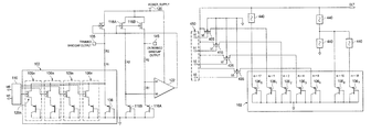
- FIG. 1 illustrates an example bandgap generation circuit 102 which can be controlled by a microcontroller 101 or any other type of microprocessor or controller and which is coupled to an untrimmed bandgap generation circuit 104 .
- Trimmed bandgap generation circuit 102 is configurable, for example, through microcontroller 101 or any other processor or controller, to provide a large trim range (e.g., 100 mV), small curvature variations, low current for low power applications (e.g., 1 ⁇ A), in accordance with certain embodiment of the present disclosure.
- Untrimmed bandgap generation circuit 104 may include a plurality of bipolar junction transistors (BJTs) 116 coupled in series to one or more resistors (R 1 , R 2 ). In the embodiment shown in FIG.
- BJTs bipolar junction transistors
- a first branch includes metal oxide semiconductor field effect transistor (MOSFET) 118 A for providing current I.
- the first branch further includes series coupled resistors R 1 and R 2 coupled with BJT 116 A on one hand and with the MOSFET 118 A on the other hand which is coupled in series with a power supply 120 .
- the second branch consists of series coupled MOSFET 118 B, resistor R 2 , and BJT 116 B.
- MOSFET transistors 118 A and B are controlled to provide the current I for each branch of the bandgap generation circuit 104 .
- Untrimmed bandgap generation circuit 104 may also include buffer 122 that controls MOSFET transistors 118 in a feedback loop. The same control signal is also fed to bandgap generation circuit 102 .
- An output of the untrimmed bandgap generation circuit can be obtained at the node 145 between transistor 118 A and resistor R 2 .
- the principle of the circuit is to generate a second voltage to the forward voltage of diode connected transistor 116 A that has an negative temperature coefficient.
- transistor 116 A may have a temperature coefficient of ⁇ 2 mV/K at 0.6 V.
- the circuit 104 can be dimensioned such that the voltage over resistors R 1 and R 2 will have a temperature coefficient of +2 mV/K. Hence, the bandgap output voltage will be nearly temperature independent. It is noted that although untrimmed bandgap generation circuit 104 may include certain circuit elements, other configurations may also be used.
- this untrimmed bandgap reference circuit 104 can be combined with bandgap generation circuit 102 to also provide for a trimmed bandgap reference voltage output 135 .
- this additional trimmable bandgap generation circuit 102 may include one or more bipolar diode elements.
- Bandgap generation circuit 102 may include bipolar diode 106 coupled in series with a first resistor 1 (R 1 ) and a second resistor (R 2 ).
- the output 135 provides for an additional trimmed bandgap output voltage as will be explained below.
- V BGT is the trimmed bandgap output
- I is the current
- R 1 and R 2 is the resistor value for the resistors in the bandgap generation circuit 102
- V BE is base-emitter voltage
- N is the number of bipolar diodes used in the trimming process. From Eq. 2, the trimmed bandgap output voltage-current can be adjusted based on the number of bipolar diodes (N) used, while keeping V BGT constant as a function of T (Temperature), as shown below with respect to Eq. 3.
- V BGT I *( R 1+ R 2)+ V T *ln [ I /( N*I s )]
- V BGT I *( R 1+ R 2)+ V T *ln [ I /( N*I s )]
- V BGT V BG ⁇ V T *ln( N ) Eq. 10 If Eq.
- the trimmed bandgap output voltage-current may be a function of the number of bipolar diodes (N) used in bandgap generation circuit 102 .
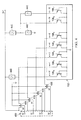
- this embodiment of bandgap generation circuit 102 may include one or multiple further bipolar diodes 106 n which can be coupled in parallel to transistor 106 .
- a digitally controllable selection circuit 110 may be provided to connect each additional transistor 106 n in parallel with transistor 106 .
- each additional set may include a metal oxide semiconductor field effect transistor (MOSFET) 126 n coupled in series with a bipolar junction transistor (BJT) 115 (e.g., PNP transistor or a NPN transistor) 106 n , wherein each set consisting of bipolar diode 106 n and MOSFET 126 n may be coupled in parallel with another set and with BJT 106 . While four sets of the MOSFET-BJT trimming branches are shown in FIG. 3 , any number of bipolar diodes 106 / 106 n may be used to trim the bandgap offset.
- MOSFET metal oxide semiconductor field effect transistor
- BJT bipolar junction transistor
- Selection circuit 110 can be controlled by a microcontroller (not shown) to adjust the reference 120 output voltage of the bandgap reference circuit 102 and may contain non-volatile memory. Thus, depending on a digital input signal at selection circuit 110 , 0, 1, 2, 3, or 4 transistors 106 n will be coupled in parallel to transistor 106 thereby providing different reference output voltages at output 135 .
- the selection circuit 110 may simply consist of respective drivers, registers, or direct connections which pass the digital signal, for example a 4-bit signal, to transistors 126 n .
- the digital signal for example a 4-bit signal
- FIG. 4 shows a further embodiment of the relevant parts of a circuit 102 which can achieve such a variety.
- each transistor 106 1 , 106 2 , 106 3 , and 106 4 are dimensioned to each other by a factor of 2 resulting, for example in different on-resistance transistor properties of 1, 2, 4, and 8. This can be done, for example, by implementing each transistor by coupling 1, 2, 4, or 8 transistors in parallel, respectively.
- transistor 106 1 is implemented as a single transistor.
- Transistor 106 2 is implemented as two transistors 135 coupled in parallel.
- Transistor 106 3 is implemented as four transistors coupled in parallel and transistor 106 4 is implemented as eight transistors coupled in parallel.
- the on-resistance can be adjusted by other means as well known in the art.
- Transistors 405 , 415 , 425 , and 435 programmably connect each additional 140 transistor 106 1 , 106 2 , 106 3 , and 106 4 to the output of circuit 102 which is coupled with transistor 106 as shown in FIG. 3 .
- one or more further transistor 106 5 , 106 6 , and 106 7 can be added optionally by fuses 440 . Depending on the configuration these transistors 106 5 , 106 6 , and 106 7 can provide for extended reference voltage ranges.
- FIG. 5 shows the variety of trimmable output voltages depending on the temperature.
- the x-axis designates a temperature range from ⁇ 50 to 150° C. and the y-axis designates the various bandgap output voltages at output 135 and 145 .
- the different symbols designating the different curves refer to different programming words.
- FIG. 5 shows different numbers “xpnp” which refer to the combined factor m of in this case activated PNP transistors 106 1 , 106 2 , 106 3 , 106 4 , 106 5 , 106 6 , and 106 7 . With the embodiment shown in FIG. 4 , only some sets of these curves are available depending on the setting of the fuses.
- Curve bg_raw designates the untrimmed output voltage at 145 .
Landscapes
- Engineering & Computer Science (AREA)
- Microelectronics & Electronic Packaging (AREA)
- Physics & Mathematics (AREA)
- Nonlinear Science (AREA)
- Electromagnetism (AREA)
- General Physics & Mathematics (AREA)
- Radar, Positioning & Navigation (AREA)
- Automation & Control Theory (AREA)
- Power Engineering (AREA)
- Control Of Electrical Variables (AREA)
- Semiconductor Integrated Circuits (AREA)
- Design And Manufacture Of Integrated Circuits (AREA)
Abstract
Description
V BG =I*(R1+R2)+V BE Eq. 1
where VBG is the untrimmed bandgap output, I is the current, R1 and R2 is the resistor value for the resistors in the untrimmed
V BGT =I*(R1+R2)+V BE(N) Eq. 2
where VBGT is the trimmed bandgap output, I is the current, R1 and R2 is the resistor value for the resistors in the
I=I s*exp(V BE /V T) Eq. 3
where VBE is base-emitter voltage, Is is a constant value, and VT=kT/q (k is Boltzmann const, q is the electron charge, and T is temperature in Kelvin),
V BE =V T*ln(I/I S) Eq. 4
where ln is natural logarithm function and
V BE(N)=V T*ln [I/(N*I s)] Eq. 5.
Substituting Eq. 4 into Eq. 1,
V BG =I*(R1+R2)+V T*ln(I/I S) Eq. 6
Substituting Eq. 5 into Eq. 2 yields
V BGT =I*(R1+R2)+V T*ln [I/(N*I s)] Eq. 7
Given that ln(a/b)=ln(a)−ln(b) and ln(a*b)=ln(a)+ln(b) Eq. 7 may be simplified to
V BGT =I*(R1+R2)+V T*(ln(I)−ln(N*I s))=I*(R1+R2)+V T*{ln(I)−ln(N)−ln(I s)} Eq. 8
or
V BGT =I*(R1+R2)+V T*(ln(I)−ln(Is))−V T*ln(N)=I*(R1+R2)+VT*ln(I/I s)−V T*ln(N) Eq. 9
Replacing the first two expression from Eq. 9 which equals Eq. 6,
V BGT =V BG −V T*ln(N) Eq. 10
If Eq. 10 is differentiated on both sides of the equation and with respect to T (temperature)
d/dT(V BGT)=d/dT(V BG)−d/dT(V T)=d/dT(V BG)−(k/q)*ln N Eq. 11
where VT=kT/q. k/q*ln N may be a very small number thus
d/dT(V BGT) is substantially equal to d/dT(V BG) Eq. 12.
Eq. 12 shows that the rate of change of trimmed bandgap voltage over temperature is approximately the same as the rate of change of the untrimmed bandgap voltage over temperature.
Claims (22)
Priority Applications (6)
| Application Number | Priority Date | Filing Date | Title |
|---|---|---|---|
| US12/613,284 US8022751B2 (en) | 2008-11-18 | 2009-11-05 | Systems and methods for trimming bandgap offset with bipolar elements |
| EP09753302.0A EP2359210B1 (en) | 2008-11-18 | 2009-11-17 | Systems and methods for trimming bandgap offset with bipolar diode elements |
| PCT/US2009/064756 WO2010059609A1 (en) | 2008-11-18 | 2009-11-17 | Systems and methods for trimming bandgap offset with bipolar diode elements |
| CN200980145533.6A CN102216868B (en) | 2008-11-18 | 2009-11-17 | For using the system and method for bipolar diode element finishing bandgap offset |
| KR1020117006004A KR101813999B1 (en) | 2008-11-18 | 2009-11-17 | Systems and methods for trimming bandgap offset with bipolar diode elements |
| TW098139187A TWI481990B (en) | 2008-11-18 | 2009-11-18 | Integrated circuit, systems and methods for trimming bandgap offset with bipolar diode elements |
Applications Claiming Priority (2)
| Application Number | Priority Date | Filing Date | Title |
|---|---|---|---|
| US11563108P | 2008-11-18 | 2008-11-18 | |
| US12/613,284 US8022751B2 (en) | 2008-11-18 | 2009-11-05 | Systems and methods for trimming bandgap offset with bipolar elements |
Publications (2)
| Publication Number | Publication Date |
|---|---|
| US20100123514A1 US20100123514A1 (en) | 2010-05-20 |
| US8022751B2 true US8022751B2 (en) | 2011-09-20 |
Family
ID=42171523
Family Applications (1)
| Application Number | Title | Priority Date | Filing Date |
|---|---|---|---|
| US12/613,284 Active US8022751B2 (en) | 2008-11-18 | 2009-11-05 | Systems and methods for trimming bandgap offset with bipolar elements |
Country Status (6)
| Country | Link |
|---|---|
| US (1) | US8022751B2 (en) |
| EP (1) | EP2359210B1 (en) |
| KR (1) | KR101813999B1 (en) |
| CN (1) | CN102216868B (en) |
| TW (1) | TWI481990B (en) |
| WO (1) | WO2010059609A1 (en) |
Cited By (10)
| Publication number | Priority date | Publication date | Assignee | Title |
|---|---|---|---|---|
| US20110084681A1 (en) * | 2009-10-08 | 2011-04-14 | Intersil Americas Inc. | Circuits and methods to produce a vptat and/or a bandgap voltage with low-glitch preconditioning |
| US20110163799A1 (en) * | 2010-01-04 | 2011-07-07 | Hong Kong Applied Science & Technology Research Institute Company Limited | Bi-directional Trimming Methods and Circuits for a Precise Band-Gap Reference |
| US20120169413A1 (en) * | 2010-12-30 | 2012-07-05 | Stmicroelectronics Inc. | Bandgap voltage reference circuit, system, and method for reduced output curvature |
| US20120286848A1 (en) * | 2011-05-13 | 2012-11-15 | Stmicroelectronics S.R.I. | Electronic trimming circuit |
| US9063556B2 (en) | 2013-02-11 | 2015-06-23 | Omnivision Technologies, Inc. | Bandgap reference circuit with offset voltage removal |
| US20170177017A1 (en) * | 2012-05-15 | 2017-06-22 | Taiwan Semiconductor Manufacturing Company, Ltd. | Bandgap reference circuit |
| US9971376B2 (en) * | 2016-10-07 | 2018-05-15 | Kilopass Technology, Inc. | Voltage reference circuits with programmable temperature slope and independent offset control |
| US10348322B1 (en) | 2018-06-26 | 2019-07-09 | Nxp Usa, Inc. | On-chip trimming circuit and method therefor |
| US10838443B2 (en) | 2018-12-05 | 2020-11-17 | Qualcomm Incorporated | Precision bandgap reference with trim adjustment |
| US20240288890A1 (en) * | 2023-02-23 | 2024-08-29 | Texas Instruments Incorporated | Bandgap reference circuit |
Families Citing this family (11)
| Publication number | Priority date | Publication date | Assignee | Title |
|---|---|---|---|---|
| JP5492702B2 (en) * | 2010-08-25 | 2014-05-14 | ルネサスエレクトロニクス株式会社 | Semiconductor device |
| US20120206192A1 (en) * | 2011-02-15 | 2012-08-16 | Fletcher Jay B | Programmable bandgap voltage reference |
| JP5635935B2 (en) * | 2011-03-31 | 2014-12-03 | ルネサスエレクトロニクス株式会社 | Constant current generation circuit, microprocessor and semiconductor device including the same |
| US9535446B2 (en) * | 2011-07-13 | 2017-01-03 | Analog Devices, Inc. | System and method for power trimming a bandgap circuit |
| EP2905672A1 (en) * | 2014-02-11 | 2015-08-12 | Dialog Semiconductor GmbH | An apparatus and method for a modified brokaw bandgap reference circuit for improved low voltage power supply |
| CN108279727B (en) * | 2017-12-25 | 2021-09-21 | 南京中感微电子有限公司 | Improved current generating circuit |
| US11233513B2 (en) | 2019-11-05 | 2022-01-25 | Mediatek Inc. | Reference voltage buffer with settling enhancement |
| US11574657B2 (en) * | 2020-09-28 | 2023-02-07 | Taiwan Semiconductor Manufacturing Company, Ltd. | Memory device, sense amplifier and method for mismatch compensation |
| US12271216B2 (en) | 2020-12-03 | 2025-04-08 | Analog Devices, Inc. | Logarithmic current to voltage converters |
| KR102907658B1 (en) | 2021-06-30 | 2026-01-05 | 삼성전자주식회사 | Read reference current generator |
| KR102907659B1 (en) | 2021-07-16 | 2026-01-06 | 삼성전자주식회사 | Nonvolatile memory device |
Citations (18)
| Publication number | Priority date | Publication date | Assignee | Title |
|---|---|---|---|---|
| US5325045A (en) * | 1993-02-17 | 1994-06-28 | Exar Corporation | Low voltage CMOS bandgap with new trimming and curvature correction methods |
| US6018272A (en) * | 1997-01-02 | 2000-01-25 | Lucent Technologies Inc. | Linearization of resistance |
| US6163199A (en) * | 1999-01-29 | 2000-12-19 | Fairchild Semiconductor Corp. | Overvoltage/undervoltage tolerant transfer gate |
| JP2001217393A (en) | 2000-02-02 | 2001-08-10 | Hitachi Ltd | CMOS integrated circuit |
| US6590372B1 (en) * | 2002-02-19 | 2003-07-08 | Texas Advanced Optoelectronic Solutions, Inc. | Method and integrated circuit for bandgap trimming |
| US6608472B1 (en) | 2000-10-26 | 2003-08-19 | Cypress Semiconductor Corporation | Band-gap reference circuit for providing an accurate reference voltage compensated for process state, process variations and temperature |
| US6870421B2 (en) * | 2002-03-15 | 2005-03-22 | Seiko Epson Corporation | Temperature characteristic compensation apparatus |
| US6894473B1 (en) * | 2003-03-05 | 2005-05-17 | Advanced Micro Devices, Inc. | Fast bandgap reference circuit for use in a low power supply A/D booster |
| US20060164158A1 (en) * | 2005-01-25 | 2006-07-27 | Nec Electronics Corporation | Reference voltage circuit |
| US7119414B2 (en) * | 2003-01-09 | 2006-10-10 | Oki Electric Industry Co., Ltd. | Fuse layout and method trimming |
| US7151414B2 (en) * | 2005-01-26 | 2006-12-19 | Texas Instruments Incorporated | Method and circuit for frequency synthesis using a low drift current controlled oscillator with wide output frequency range |
| US20060285414A1 (en) | 2005-06-20 | 2006-12-21 | Hiroyuki Kimura | Fuse circuit and electronic circuit |
| US20070098041A1 (en) | 2005-08-10 | 2007-05-03 | Samsung Electronics Co., Ltd. | On chip temperature detector, temperature detection method and refresh control method using the same |
| US20080084240A1 (en) * | 2006-10-10 | 2008-04-10 | Atmel Corporation | Apparatus and method for providing a temperature compensated reference current |
| US7443226B1 (en) * | 2005-11-22 | 2008-10-28 | National Semiconductor Corporation | Emitter area trim scheme for a PTAT current source |
| US7463012B2 (en) * | 2006-11-20 | 2008-12-09 | Micrel, Incorporated | Bandgap reference circuits with isolated trim elements |
| US7538597B2 (en) * | 2007-08-13 | 2009-05-26 | Hong Kong Applied Science And Technology Research Institute Co. Ltd. | Fuse cell and method for programming the same |
| US7880459B2 (en) * | 2007-05-11 | 2011-02-01 | Intersil Americas Inc. | Circuits and methods to produce a VPTAT and/or a bandgap voltage |
Family Cites Families (4)
| Publication number | Priority date | Publication date | Assignee | Title |
|---|---|---|---|---|
| EP0986105B1 (en) * | 1998-09-07 | 2005-11-30 | STMicroelectronics S.r.l. | Electronic circuit for trimming integrated circuits |
| JP4413406B2 (en) * | 2000-10-03 | 2010-02-10 | 株式会社東芝 | Nonvolatile semiconductor memory and test method thereof |
| US7224209B2 (en) * | 2005-03-03 | 2007-05-29 | Etron Technology, Inc. | Speed-up circuit for initiation of proportional to absolute temperature biasing circuits |
| US7633333B2 (en) * | 2006-11-16 | 2009-12-15 | Infineon Technologies Ag | Systems, apparatus and methods relating to bandgap circuits |
-
2009
- 2009-11-05 US US12/613,284 patent/US8022751B2/en active Active
- 2009-11-17 KR KR1020117006004A patent/KR101813999B1/en active Active
- 2009-11-17 WO PCT/US2009/064756 patent/WO2010059609A1/en not_active Ceased
- 2009-11-17 EP EP09753302.0A patent/EP2359210B1/en active Active
- 2009-11-17 CN CN200980145533.6A patent/CN102216868B/en active Active
- 2009-11-18 TW TW098139187A patent/TWI481990B/en active
Patent Citations (18)
| Publication number | Priority date | Publication date | Assignee | Title |
|---|---|---|---|---|
| US5325045A (en) * | 1993-02-17 | 1994-06-28 | Exar Corporation | Low voltage CMOS bandgap with new trimming and curvature correction methods |
| US6018272A (en) * | 1997-01-02 | 2000-01-25 | Lucent Technologies Inc. | Linearization of resistance |
| US6163199A (en) * | 1999-01-29 | 2000-12-19 | Fairchild Semiconductor Corp. | Overvoltage/undervoltage tolerant transfer gate |
| JP2001217393A (en) | 2000-02-02 | 2001-08-10 | Hitachi Ltd | CMOS integrated circuit |
| US6608472B1 (en) | 2000-10-26 | 2003-08-19 | Cypress Semiconductor Corporation | Band-gap reference circuit for providing an accurate reference voltage compensated for process state, process variations and temperature |
| US6590372B1 (en) * | 2002-02-19 | 2003-07-08 | Texas Advanced Optoelectronic Solutions, Inc. | Method and integrated circuit for bandgap trimming |
| US6870421B2 (en) * | 2002-03-15 | 2005-03-22 | Seiko Epson Corporation | Temperature characteristic compensation apparatus |
| US7119414B2 (en) * | 2003-01-09 | 2006-10-10 | Oki Electric Industry Co., Ltd. | Fuse layout and method trimming |
| US6894473B1 (en) * | 2003-03-05 | 2005-05-17 | Advanced Micro Devices, Inc. | Fast bandgap reference circuit for use in a low power supply A/D booster |
| US20060164158A1 (en) * | 2005-01-25 | 2006-07-27 | Nec Electronics Corporation | Reference voltage circuit |
| US7151414B2 (en) * | 2005-01-26 | 2006-12-19 | Texas Instruments Incorporated | Method and circuit for frequency synthesis using a low drift current controlled oscillator with wide output frequency range |
| US20060285414A1 (en) | 2005-06-20 | 2006-12-21 | Hiroyuki Kimura | Fuse circuit and electronic circuit |
| US20070098041A1 (en) | 2005-08-10 | 2007-05-03 | Samsung Electronics Co., Ltd. | On chip temperature detector, temperature detection method and refresh control method using the same |
| US7443226B1 (en) * | 2005-11-22 | 2008-10-28 | National Semiconductor Corporation | Emitter area trim scheme for a PTAT current source |
| US20080084240A1 (en) * | 2006-10-10 | 2008-04-10 | Atmel Corporation | Apparatus and method for providing a temperature compensated reference current |
| US7463012B2 (en) * | 2006-11-20 | 2008-12-09 | Micrel, Incorporated | Bandgap reference circuits with isolated trim elements |
| US7880459B2 (en) * | 2007-05-11 | 2011-02-01 | Intersil Americas Inc. | Circuits and methods to produce a VPTAT and/or a bandgap voltage |
| US7538597B2 (en) * | 2007-08-13 | 2009-05-26 | Hong Kong Applied Science And Technology Research Institute Co. Ltd. | Fuse cell and method for programming the same |
Non-Patent Citations (1)
| Title |
|---|
| International PCT Search Report, PCT/US2009/064756, 14 pages, mailed Mar. 11, 2010. |
Cited By (15)
| Publication number | Priority date | Publication date | Assignee | Title |
|---|---|---|---|---|
| US8330445B2 (en) * | 2009-10-08 | 2012-12-11 | Intersil Americas Inc. | Circuits and methods to produce a VPTAT and/or a bandgap voltage with low-glitch preconditioning |
| US20110084681A1 (en) * | 2009-10-08 | 2011-04-14 | Intersil Americas Inc. | Circuits and methods to produce a vptat and/or a bandgap voltage with low-glitch preconditioning |
| US20110163799A1 (en) * | 2010-01-04 | 2011-07-07 | Hong Kong Applied Science & Technology Research Institute Company Limited | Bi-directional Trimming Methods and Circuits for a Precise Band-Gap Reference |
| US8193854B2 (en) * | 2010-01-04 | 2012-06-05 | Hong Kong Applied Science and Technology Research Institute Company, Ltd. | Bi-directional trimming methods and circuits for a precise band-gap reference |
| US8648648B2 (en) * | 2010-12-30 | 2014-02-11 | Stmicroelectronics, Inc. | Bandgap voltage reference circuit, system, and method for reduced output curvature |
| US20120169413A1 (en) * | 2010-12-30 | 2012-07-05 | Stmicroelectronics Inc. | Bandgap voltage reference circuit, system, and method for reduced output curvature |
| US20120286848A1 (en) * | 2011-05-13 | 2012-11-15 | Stmicroelectronics S.R.I. | Electronic trimming circuit |
| US8665006B2 (en) * | 2011-05-13 | 2014-03-04 | Stmicroelectronics S.R.L. | Electronic trimming circuit |
| US20170177017A1 (en) * | 2012-05-15 | 2017-06-22 | Taiwan Semiconductor Manufacturing Company, Ltd. | Bandgap reference circuit |
| US10296032B2 (en) * | 2012-05-15 | 2019-05-21 | Taiwan Semiconductor Manufacturing Company, Ltd. | Bandgap reference circuit |
| US9063556B2 (en) | 2013-02-11 | 2015-06-23 | Omnivision Technologies, Inc. | Bandgap reference circuit with offset voltage removal |
| US9971376B2 (en) * | 2016-10-07 | 2018-05-15 | Kilopass Technology, Inc. | Voltage reference circuits with programmable temperature slope and independent offset control |
| US10348322B1 (en) | 2018-06-26 | 2019-07-09 | Nxp Usa, Inc. | On-chip trimming circuit and method therefor |
| US10838443B2 (en) | 2018-12-05 | 2020-11-17 | Qualcomm Incorporated | Precision bandgap reference with trim adjustment |
| US20240288890A1 (en) * | 2023-02-23 | 2024-08-29 | Texas Instruments Incorporated | Bandgap reference circuit |
Also Published As
| Publication number | Publication date |
|---|---|
| CN102216868B (en) | 2016-08-03 |
| TWI481990B (en) | 2015-04-21 |
| EP2359210A1 (en) | 2011-08-24 |
| EP2359210B1 (en) | 2021-01-27 |
| US20100123514A1 (en) | 2010-05-20 |
| TW201032016A (en) | 2010-09-01 |
| KR101813999B1 (en) | 2018-01-02 |
| KR20110091848A (en) | 2011-08-16 |
| CN102216868A (en) | 2011-10-12 |
| WO2010059609A1 (en) | 2010-05-27 |
Similar Documents
| Publication | Publication Date | Title |
|---|---|---|
| US8022751B2 (en) | Systems and methods for trimming bandgap offset with bipolar elements | |
| US10642305B2 (en) | High-accuracy CMOS temperature sensor and operating method | |
| US8922190B2 (en) | Band gap reference voltage generator | |
| US20070296392A1 (en) | Bandgap reference circuits | |
| US10209732B2 (en) | Bandgap reference circuit with tunable current source | |
| EP0620515A1 (en) | Band gap reference voltage source | |
| US10684637B2 (en) | Bandgap reference voltage generating circuit with temperature correction at range of high/low temperature | |
| US10613570B1 (en) | Bandgap circuits with voltage calibration | |
| US20180074532A1 (en) | Reference voltage generator | |
| JPH11121694A (en) | Reference voltage generation circuit and adjustment method thereof | |
| US6954058B2 (en) | Constant current supply device | |
| JP2005134145A (en) | Temperature sensor circuit | |
| TWI435200B (en) | Bandgap voltage and current reference | |
| JP2005182113A (en) | Reference voltage generation circuit | |
| JP6765119B2 (en) | Reference voltage generation circuit and method | |
| US12393218B2 (en) | Switch control voltage generator, bandgap reference generator, and method for generating switch voltage thereof | |
| US20240077901A1 (en) | Reference voltage generation circuit | |
| US11977405B2 (en) | Reference voltage generator circuit such as band gap reference voltage generator circuit, and method of generating reference voltage | |
| US8278905B2 (en) | Rotating gain resistors to produce a bandgap voltage with low-drift | |
| JP4228890B2 (en) | Semiconductor integrated circuit device | |
| US6346802B2 (en) | Calibration circuit for a band-gap reference voltage | |
| JP2004110702A (en) | Band gap reference circuit | |
| US9588538B2 (en) | Reference voltage generation circuit | |
| KR101231248B1 (en) | static voltage generating circuit | |
| TW202030980A (en) | Power on clear circuit |
Legal Events
| Date | Code | Title | Description |
|---|---|---|---|
| AS | Assignment |
Owner name: MICROCHIP TECHNOLOGY INCORPORATED,ARIZONA Free format text: ASSIGNMENT OF ASSIGNORS INTEREST;ASSIGNORS:LE, MINH;MARTIN, WOOWAI;REEL/FRAME:023478/0109 Effective date: 20091019 Owner name: MICROCHIP TECHNOLOGY INCORPORATED, ARIZONA Free format text: ASSIGNMENT OF ASSIGNORS INTEREST;ASSIGNORS:LE, MINH;MARTIN, WOOWAI;REEL/FRAME:023478/0109 Effective date: 20091019 |
|
| STCF | Information on status: patent grant |
Free format text: PATENTED CASE |
|
| FPAY | Fee payment |
Year of fee payment: 4 |
|
| AS | Assignment |
Owner name: JPMORGAN CHASE BANK, N.A., AS ADMINISTRATIVE AGENT, ILLINOIS Free format text: SECURITY INTEREST;ASSIGNOR:MICROCHIP TECHNOLOGY INCORPORATED;REEL/FRAME:041675/0617 Effective date: 20170208 Owner name: JPMORGAN CHASE BANK, N.A., AS ADMINISTRATIVE AGENT Free format text: SECURITY INTEREST;ASSIGNOR:MICROCHIP TECHNOLOGY INCORPORATED;REEL/FRAME:041675/0617 Effective date: 20170208 |
|
| AS | Assignment |
Owner name: JPMORGAN CHASE BANK, N.A., AS ADMINISTRATIVE AGENT, ILLINOIS Free format text: SECURITY INTEREST;ASSIGNORS:MICROCHIP TECHNOLOGY INCORPORATED;SILICON STORAGE TECHNOLOGY, INC.;ATMEL CORPORATION;AND OTHERS;REEL/FRAME:046426/0001 Effective date: 20180529 Owner name: JPMORGAN CHASE BANK, N.A., AS ADMINISTRATIVE AGENT Free format text: SECURITY INTEREST;ASSIGNORS:MICROCHIP TECHNOLOGY INCORPORATED;SILICON STORAGE TECHNOLOGY, INC.;ATMEL CORPORATION;AND OTHERS;REEL/FRAME:046426/0001 Effective date: 20180529 |
|
| AS | Assignment |
Owner name: WELLS FARGO BANK, NATIONAL ASSOCIATION, AS NOTES COLLATERAL AGENT, CALIFORNIA Free format text: SECURITY INTEREST;ASSIGNORS:MICROCHIP TECHNOLOGY INCORPORATED;SILICON STORAGE TECHNOLOGY, INC.;ATMEL CORPORATION;AND OTHERS;REEL/FRAME:047103/0206 Effective date: 20180914 Owner name: WELLS FARGO BANK, NATIONAL ASSOCIATION, AS NOTES C Free format text: SECURITY INTEREST;ASSIGNORS:MICROCHIP TECHNOLOGY INCORPORATED;SILICON STORAGE TECHNOLOGY, INC.;ATMEL CORPORATION;AND OTHERS;REEL/FRAME:047103/0206 Effective date: 20180914 |
|
| MAFP | Maintenance fee payment |
Free format text: PAYMENT OF MAINTENANCE FEE, 8TH YEAR, LARGE ENTITY (ORIGINAL EVENT CODE: M1552); ENTITY STATUS OF PATENT OWNER: LARGE ENTITY Year of fee payment: 8 |
|
| AS | Assignment |
Owner name: JPMORGAN CHASE BANK, N.A., AS ADMINISTRATIVE AGENT, DELAWARE Free format text: SECURITY INTEREST;ASSIGNORS:MICROCHIP TECHNOLOGY INC.;SILICON STORAGE TECHNOLOGY, INC.;ATMEL CORPORATION;AND OTHERS;REEL/FRAME:053311/0305 Effective date: 20200327 |
|
| AS | Assignment |
Owner name: MICROSEMI CORPORATION, CALIFORNIA Free format text: RELEASE BY SECURED PARTY;ASSIGNOR:JPMORGAN CHASE BANK, N.A, AS ADMINISTRATIVE AGENT;REEL/FRAME:053466/0011 Effective date: 20200529 Owner name: ATMEL CORPORATION, ARIZONA Free format text: RELEASE BY SECURED PARTY;ASSIGNOR:JPMORGAN CHASE BANK, N.A, AS ADMINISTRATIVE AGENT;REEL/FRAME:053466/0011 Effective date: 20200529 Owner name: MICROSEMI STORAGE SOLUTIONS, INC., ARIZONA Free format text: RELEASE BY SECURED PARTY;ASSIGNOR:JPMORGAN CHASE BANK, N.A, AS ADMINISTRATIVE AGENT;REEL/FRAME:053466/0011 Effective date: 20200529 Owner name: MICROCHIP TECHNOLOGY INC., ARIZONA Free format text: RELEASE BY SECURED PARTY;ASSIGNOR:JPMORGAN CHASE BANK, N.A, AS ADMINISTRATIVE AGENT;REEL/FRAME:053466/0011 Effective date: 20200529 Owner name: SILICON STORAGE TECHNOLOGY, INC., ARIZONA Free format text: RELEASE BY SECURED PARTY;ASSIGNOR:JPMORGAN CHASE BANK, N.A, AS ADMINISTRATIVE AGENT;REEL/FRAME:053466/0011 Effective date: 20200529 |
|
| AS | Assignment |
Owner name: WELLS FARGO BANK, NATIONAL ASSOCIATION, MINNESOTA Free format text: SECURITY INTEREST;ASSIGNORS:MICROCHIP TECHNOLOGY INC.;SILICON STORAGE TECHNOLOGY, INC.;ATMEL CORPORATION;AND OTHERS;REEL/FRAME:053468/0705 Effective date: 20200529 |
|
| AS | Assignment |
Owner name: WELLS FARGO BANK, NATIONAL ASSOCIATION, AS COLLATERAL AGENT, MINNESOTA Free format text: SECURITY INTEREST;ASSIGNORS:MICROCHIP TECHNOLOGY INCORPORATED;SILICON STORAGE TECHNOLOGY, INC.;ATMEL CORPORATION;AND OTHERS;REEL/FRAME:055671/0612 Effective date: 20201217 |
|
| AS | Assignment |
Owner name: WELLS FARGO BANK, NATIONAL ASSOCIATION, AS NOTES COLLATERAL AGENT, MINNESOTA Free format text: SECURITY INTEREST;ASSIGNORS:MICROCHIP TECHNOLOGY INCORPORATED;SILICON STORAGE TECHNOLOGY, INC.;ATMEL CORPORATION;AND OTHERS;REEL/FRAME:057935/0474 Effective date: 20210528 |
|
| AS | Assignment |
Owner name: MICROSEMI STORAGE SOLUTIONS, INC., ARIZONA Free format text: RELEASE BY SECURED PARTY;ASSIGNOR:JPMORGAN CHASE BANK, N.A., AS ADMINISTRATIVE AGENT;REEL/FRAME:059333/0222 Effective date: 20220218 Owner name: MICROSEMI CORPORATION, ARIZONA Free format text: RELEASE BY SECURED PARTY;ASSIGNOR:JPMORGAN CHASE BANK, N.A., AS ADMINISTRATIVE AGENT;REEL/FRAME:059333/0222 Effective date: 20220218 Owner name: ATMEL CORPORATION, ARIZONA Free format text: RELEASE BY SECURED PARTY;ASSIGNOR:JPMORGAN CHASE BANK, N.A., AS ADMINISTRATIVE AGENT;REEL/FRAME:059333/0222 Effective date: 20220218 Owner name: SILICON STORAGE TECHNOLOGY, INC., ARIZONA Free format text: RELEASE BY SECURED PARTY;ASSIGNOR:JPMORGAN CHASE BANK, N.A., AS ADMINISTRATIVE AGENT;REEL/FRAME:059333/0222 Effective date: 20220218 Owner name: MICROCHIP TECHNOLOGY INCORPORATED, ARIZONA Free format text: RELEASE BY SECURED PARTY;ASSIGNOR:JPMORGAN CHASE BANK, N.A., AS ADMINISTRATIVE AGENT;REEL/FRAME:059333/0222 Effective date: 20220218 Owner name: MICROCHIP TECHNOLOGY INCORPORATED, ARIZONA Free format text: RELEASE OF SECURITY INTEREST;ASSIGNOR:JPMORGAN CHASE BANK, N.A., AS ADMINISTRATIVE AGENT;REEL/FRAME:059333/0222 Effective date: 20220218 Owner name: SILICON STORAGE TECHNOLOGY, INC., ARIZONA Free format text: RELEASE OF SECURITY INTEREST;ASSIGNOR:JPMORGAN CHASE BANK, N.A., AS ADMINISTRATIVE AGENT;REEL/FRAME:059333/0222 Effective date: 20220218 Owner name: ATMEL CORPORATION, ARIZONA Free format text: RELEASE OF SECURITY INTEREST;ASSIGNOR:JPMORGAN CHASE BANK, N.A., AS ADMINISTRATIVE AGENT;REEL/FRAME:059333/0222 Effective date: 20220218 Owner name: MICROSEMI CORPORATION, ARIZONA Free format text: RELEASE OF SECURITY INTEREST;ASSIGNOR:JPMORGAN CHASE BANK, N.A., AS ADMINISTRATIVE AGENT;REEL/FRAME:059333/0222 Effective date: 20220218 Owner name: MICROSEMI STORAGE SOLUTIONS, INC., ARIZONA Free format text: RELEASE OF SECURITY INTEREST;ASSIGNOR:JPMORGAN CHASE BANK, N.A., AS ADMINISTRATIVE AGENT;REEL/FRAME:059333/0222 Effective date: 20220218 |
|
| AS | Assignment |
Owner name: MICROCHIP TECHNOLOGY INCORPORATED, ARIZONA Free format text: RELEASE BY SECURED PARTY;ASSIGNOR:JPMORGAN CHASE BANK, N.A., AS ADMINISTRATIVE AGENT;REEL/FRAME:059666/0545 Effective date: 20220218 |
|
| AS | Assignment |
Owner name: MICROSEMI STORAGE SOLUTIONS, INC., ARIZONA Free format text: RELEASE BY SECURED PARTY;ASSIGNOR:WELLS FARGO BANK, NATIONAL ASSOCIATION, AS NOTES COLLATERAL AGENT;REEL/FRAME:059358/0001 Effective date: 20220228 Owner name: MICROSEMI CORPORATION, ARIZONA Free format text: RELEASE BY SECURED PARTY;ASSIGNOR:WELLS FARGO BANK, NATIONAL ASSOCIATION, AS NOTES COLLATERAL AGENT;REEL/FRAME:059358/0001 Effective date: 20220228 Owner name: ATMEL CORPORATION, ARIZONA Free format text: RELEASE BY SECURED PARTY;ASSIGNOR:WELLS FARGO BANK, NATIONAL ASSOCIATION, AS NOTES COLLATERAL AGENT;REEL/FRAME:059358/0001 Effective date: 20220228 Owner name: SILICON STORAGE TECHNOLOGY, INC., ARIZONA Free format text: RELEASE BY SECURED PARTY;ASSIGNOR:WELLS FARGO BANK, NATIONAL ASSOCIATION, AS NOTES COLLATERAL AGENT;REEL/FRAME:059358/0001 Effective date: 20220228 Owner name: MICROCHIP TECHNOLOGY INCORPORATED, ARIZONA Free format text: RELEASE BY SECURED PARTY;ASSIGNOR:WELLS FARGO BANK, NATIONAL ASSOCIATION, AS NOTES COLLATERAL AGENT;REEL/FRAME:059358/0001 Effective date: 20220228 Owner name: MICROCHIP TECHNOLOGY INCORPORATED, ARIZONA Free format text: RELEASE OF SECURITY INTEREST;ASSIGNOR:WELLS FARGO BANK, NATIONAL ASSOCIATION, AS NOTES COLLATERAL AGENT;REEL/FRAME:059358/0001 Effective date: 20220228 Owner name: SILICON STORAGE TECHNOLOGY, INC., ARIZONA Free format text: RELEASE OF SECURITY INTEREST;ASSIGNOR:WELLS FARGO BANK, NATIONAL ASSOCIATION, AS NOTES COLLATERAL AGENT;REEL/FRAME:059358/0001 Effective date: 20220228 Owner name: ATMEL CORPORATION, ARIZONA Free format text: RELEASE OF SECURITY INTEREST;ASSIGNOR:WELLS FARGO BANK, NATIONAL ASSOCIATION, AS NOTES COLLATERAL AGENT;REEL/FRAME:059358/0001 Effective date: 20220228 Owner name: MICROSEMI CORPORATION, ARIZONA Free format text: RELEASE OF SECURITY INTEREST;ASSIGNOR:WELLS FARGO BANK, NATIONAL ASSOCIATION, AS NOTES COLLATERAL AGENT;REEL/FRAME:059358/0001 Effective date: 20220228 Owner name: MICROSEMI STORAGE SOLUTIONS, INC., ARIZONA Free format text: RELEASE OF SECURITY INTEREST;ASSIGNOR:WELLS FARGO BANK, NATIONAL ASSOCIATION, AS NOTES COLLATERAL AGENT;REEL/FRAME:059358/0001 Effective date: 20220228 |
|
| AS | Assignment |
Owner name: MICROSEMI STORAGE SOLUTIONS, INC., ARIZONA Free format text: RELEASE BY SECURED PARTY;ASSIGNOR:WELLS FARGO BANK, NATIONAL ASSOCIATION, AS NOTES COLLATERAL AGENT;REEL/FRAME:059863/0400 Effective date: 20220228 Owner name: MICROSEMI CORPORATION, ARIZONA Free format text: RELEASE BY SECURED PARTY;ASSIGNOR:WELLS FARGO BANK, NATIONAL ASSOCIATION, AS NOTES COLLATERAL AGENT;REEL/FRAME:059863/0400 Effective date: 20220228 Owner name: ATMEL CORPORATION, ARIZONA Free format text: RELEASE BY SECURED PARTY;ASSIGNOR:WELLS FARGO BANK, NATIONAL ASSOCIATION, AS NOTES COLLATERAL AGENT;REEL/FRAME:059863/0400 Effective date: 20220228 Owner name: SILICON STORAGE TECHNOLOGY, INC., ARIZONA Free format text: RELEASE BY SECURED PARTY;ASSIGNOR:WELLS FARGO BANK, NATIONAL ASSOCIATION, AS NOTES COLLATERAL AGENT;REEL/FRAME:059863/0400 Effective date: 20220228 Owner name: MICROCHIP TECHNOLOGY INCORPORATED, ARIZONA Free format text: RELEASE BY SECURED PARTY;ASSIGNOR:WELLS FARGO BANK, NATIONAL ASSOCIATION, AS NOTES COLLATERAL AGENT;REEL/FRAME:059863/0400 Effective date: 20220228 Owner name: MICROCHIP TECHNOLOGY INCORPORATED, ARIZONA Free format text: RELEASE OF SECURITY INTEREST;ASSIGNOR:WELLS FARGO BANK, NATIONAL ASSOCIATION, AS NOTES COLLATERAL AGENT;REEL/FRAME:059863/0400 Effective date: 20220228 Owner name: SILICON STORAGE TECHNOLOGY, INC., ARIZONA Free format text: RELEASE OF SECURITY INTEREST;ASSIGNOR:WELLS FARGO BANK, NATIONAL ASSOCIATION, AS NOTES COLLATERAL AGENT;REEL/FRAME:059863/0400 Effective date: 20220228 Owner name: ATMEL CORPORATION, ARIZONA Free format text: RELEASE OF SECURITY INTEREST;ASSIGNOR:WELLS FARGO BANK, NATIONAL ASSOCIATION, AS NOTES COLLATERAL AGENT;REEL/FRAME:059863/0400 Effective date: 20220228 Owner name: MICROSEMI CORPORATION, ARIZONA Free format text: RELEASE OF SECURITY INTEREST;ASSIGNOR:WELLS FARGO BANK, NATIONAL ASSOCIATION, AS NOTES COLLATERAL AGENT;REEL/FRAME:059863/0400 Effective date: 20220228 Owner name: MICROSEMI STORAGE SOLUTIONS, INC., ARIZONA Free format text: RELEASE OF SECURITY INTEREST;ASSIGNOR:WELLS FARGO BANK, NATIONAL ASSOCIATION, AS NOTES COLLATERAL AGENT;REEL/FRAME:059863/0400 Effective date: 20220228 |
|
| AS | Assignment |
Owner name: MICROSEMI STORAGE SOLUTIONS, INC., ARIZONA Free format text: RELEASE BY SECURED PARTY;ASSIGNOR:WELLS FARGO BANK, NATIONAL ASSOCIATION, AS NOTES COLLATERAL AGENT;REEL/FRAME:059363/0001 Effective date: 20220228 Owner name: MICROSEMI CORPORATION, ARIZONA Free format text: RELEASE BY SECURED PARTY;ASSIGNOR:WELLS FARGO BANK, NATIONAL ASSOCIATION, AS NOTES COLLATERAL AGENT;REEL/FRAME:059363/0001 Effective date: 20220228 Owner name: ATMEL CORPORATION, ARIZONA Free format text: RELEASE BY SECURED PARTY;ASSIGNOR:WELLS FARGO BANK, NATIONAL ASSOCIATION, AS NOTES COLLATERAL AGENT;REEL/FRAME:059363/0001 Effective date: 20220228 Owner name: SILICON STORAGE TECHNOLOGY, INC., ARIZONA Free format text: RELEASE BY SECURED PARTY;ASSIGNOR:WELLS FARGO BANK, NATIONAL ASSOCIATION, AS NOTES COLLATERAL AGENT;REEL/FRAME:059363/0001 Effective date: 20220228 Owner name: MICROCHIP TECHNOLOGY INCORPORATED, ARIZONA Free format text: RELEASE BY SECURED PARTY;ASSIGNOR:WELLS FARGO BANK, NATIONAL ASSOCIATION, AS NOTES COLLATERAL AGENT;REEL/FRAME:059363/0001 Effective date: 20220228 Owner name: MICROCHIP TECHNOLOGY INCORPORATED, ARIZONA Free format text: RELEASE OF SECURITY INTEREST;ASSIGNOR:WELLS FARGO BANK, NATIONAL ASSOCIATION, AS NOTES COLLATERAL AGENT;REEL/FRAME:059363/0001 Effective date: 20220228 Owner name: SILICON STORAGE TECHNOLOGY, INC., ARIZONA Free format text: RELEASE OF SECURITY INTEREST;ASSIGNOR:WELLS FARGO BANK, NATIONAL ASSOCIATION, AS NOTES COLLATERAL AGENT;REEL/FRAME:059363/0001 Effective date: 20220228 Owner name: ATMEL CORPORATION, ARIZONA Free format text: RELEASE OF SECURITY INTEREST;ASSIGNOR:WELLS FARGO BANK, NATIONAL ASSOCIATION, AS NOTES COLLATERAL AGENT;REEL/FRAME:059363/0001 Effective date: 20220228 Owner name: MICROSEMI CORPORATION, ARIZONA Free format text: RELEASE OF SECURITY INTEREST;ASSIGNOR:WELLS FARGO BANK, NATIONAL ASSOCIATION, AS NOTES COLLATERAL AGENT;REEL/FRAME:059363/0001 Effective date: 20220228 Owner name: MICROSEMI STORAGE SOLUTIONS, INC., ARIZONA Free format text: RELEASE OF SECURITY INTEREST;ASSIGNOR:WELLS FARGO BANK, NATIONAL ASSOCIATION, AS NOTES COLLATERAL AGENT;REEL/FRAME:059363/0001 Effective date: 20220228 |
|
| AS | Assignment |
Owner name: MICROSEMI STORAGE SOLUTIONS, INC., ARIZONA Free format text: RELEASE BY SECURED PARTY;ASSIGNOR:WELLS FARGO BANK, NATIONAL ASSOCIATION, AS NOTES COLLATERAL AGENT;REEL/FRAME:060894/0437 Effective date: 20220228 Owner name: MICROSEMI CORPORATION, ARIZONA Free format text: RELEASE BY SECURED PARTY;ASSIGNOR:WELLS FARGO BANK, NATIONAL ASSOCIATION, AS NOTES COLLATERAL AGENT;REEL/FRAME:060894/0437 Effective date: 20220228 Owner name: ATMEL CORPORATION, ARIZONA Free format text: RELEASE BY SECURED PARTY;ASSIGNOR:WELLS FARGO BANK, NATIONAL ASSOCIATION, AS NOTES COLLATERAL AGENT;REEL/FRAME:060894/0437 Effective date: 20220228 Owner name: SILICON STORAGE TECHNOLOGY, INC., ARIZONA Free format text: RELEASE BY SECURED PARTY;ASSIGNOR:WELLS FARGO BANK, NATIONAL ASSOCIATION, AS NOTES COLLATERAL AGENT;REEL/FRAME:060894/0437 Effective date: 20220228 Owner name: MICROCHIP TECHNOLOGY INCORPORATED, ARIZONA Free format text: RELEASE BY SECURED PARTY;ASSIGNOR:WELLS FARGO BANK, NATIONAL ASSOCIATION, AS NOTES COLLATERAL AGENT;REEL/FRAME:060894/0437 Effective date: 20220228 Owner name: MICROCHIP TECHNOLOGY INCORPORATED, ARIZONA Free format text: RELEASE OF SECURITY INTEREST;ASSIGNOR:WELLS FARGO BANK, NATIONAL ASSOCIATION, AS NOTES COLLATERAL AGENT;REEL/FRAME:060894/0437 Effective date: 20220228 Owner name: SILICON STORAGE TECHNOLOGY, INC., ARIZONA Free format text: RELEASE OF SECURITY INTEREST;ASSIGNOR:WELLS FARGO BANK, NATIONAL ASSOCIATION, AS NOTES COLLATERAL AGENT;REEL/FRAME:060894/0437 Effective date: 20220228 Owner name: ATMEL CORPORATION, ARIZONA Free format text: RELEASE OF SECURITY INTEREST;ASSIGNOR:WELLS FARGO BANK, NATIONAL ASSOCIATION, AS NOTES COLLATERAL AGENT;REEL/FRAME:060894/0437 Effective date: 20220228 Owner name: MICROSEMI CORPORATION, ARIZONA Free format text: RELEASE OF SECURITY INTEREST;ASSIGNOR:WELLS FARGO BANK, NATIONAL ASSOCIATION, AS NOTES COLLATERAL AGENT;REEL/FRAME:060894/0437 Effective date: 20220228 Owner name: MICROSEMI STORAGE SOLUTIONS, INC., ARIZONA Free format text: RELEASE OF SECURITY INTEREST;ASSIGNOR:WELLS FARGO BANK, NATIONAL ASSOCIATION, AS NOTES COLLATERAL AGENT;REEL/FRAME:060894/0437 Effective date: 20220228 |
|
| MAFP | Maintenance fee payment |
Free format text: PAYMENT OF MAINTENANCE FEE, 12TH YEAR, LARGE ENTITY (ORIGINAL EVENT CODE: M1553); ENTITY STATUS OF PATENT OWNER: LARGE ENTITY Year of fee payment: 12 |