US8006149B2 - System and method for device performance characterization in physical and logical domains with AC SCAN testing - Google Patents
System and method for device performance characterization in physical and logical domains with AC SCAN testing Download PDFInfo
- Publication number
- US8006149B2 US8006149B2 US11/563,612 US56361206A US8006149B2 US 8006149 B2 US8006149 B2 US 8006149B2 US 56361206 A US56361206 A US 56361206A US 8006149 B2 US8006149 B2 US 8006149B2
- Authority
- US
- United States
- Prior art keywords
- scan
- scan cell
- cell
- test
- timing
- Prior art date
- Legal status (The legal status is an assumption and is not a legal conclusion. Google has not performed a legal analysis and makes no representation as to the accuracy of the status listed.)
- Expired - Fee Related, expires
Links
- 238000012360 testing method Methods 0.000 title claims abstract description 86
- 238000000034 method Methods 0.000 title claims abstract description 31
- 238000012512 characterization method Methods 0.000 title abstract description 4
- 238000004519 manufacturing process Methods 0.000 claims abstract description 6
- 230000007547 defect Effects 0.000 claims abstract description 5
- 239000004065 semiconductor Substances 0.000 claims abstract description 5
- 238000013461 design Methods 0.000 claims description 19
- 238000005259 measurement Methods 0.000 claims description 11
- 238000010586 diagram Methods 0.000 claims description 6
- 238000010408 sweeping Methods 0.000 claims description 4
- 230000004044 response Effects 0.000 claims description 3
- 230000007704 transition Effects 0.000 claims description 3
- 230000009028 cell transition Effects 0.000 claims 1
- 230000035945 sensitivity Effects 0.000 abstract 1
- 230000008569 process Effects 0.000 description 11
- 240000007320 Pinus strobus Species 0.000 description 8
- 235000012431 wafers Nutrition 0.000 description 7
- 238000004458 analytical method Methods 0.000 description 6
- 238000013459 approach Methods 0.000 description 5
- 238000003780 insertion Methods 0.000 description 5
- 230000037431 insertion Effects 0.000 description 5
- 238000001228 spectrum Methods 0.000 description 4
- 238000013507 mapping Methods 0.000 description 2
- 239000003550 marker Substances 0.000 description 2
- 230000003542 behavioural effect Effects 0.000 description 1
- 230000008859 change Effects 0.000 description 1
- 239000012141 concentrate Substances 0.000 description 1
- 238000007405 data analysis Methods 0.000 description 1
- 238000013480 data collection Methods 0.000 description 1
- 230000006870 function Effects 0.000 description 1
- 230000008520 organization Effects 0.000 description 1
- 238000004088 simulation Methods 0.000 description 1
- 238000013519 translation Methods 0.000 description 1
- 239000013598 vector Substances 0.000 description 1
Images


Classifications
-
- G—PHYSICS
- G01—MEASURING; TESTING
- G01R—MEASURING ELECTRIC VARIABLES; MEASURING MAGNETIC VARIABLES
- G01R31/00—Arrangements for testing electric properties; Arrangements for locating electric faults; Arrangements for electrical testing characterised by what is being tested not provided for elsewhere
- G01R31/28—Testing of electronic circuits, e.g. by signal tracer
- G01R31/317—Testing of digital circuits
- G01R31/3181—Functional testing
- G01R31/3185—Reconfiguring for testing, e.g. LSSD, partitioning
- G01R31/318533—Reconfiguring for testing, e.g. LSSD, partitioning using scanning techniques, e.g. LSSD, Boundary Scan, JTAG
- G01R31/318544—Scanning methods, algorithms and patterns
- G01R31/318547—Data generators or compressors
-
- G—PHYSICS
- G01—MEASURING; TESTING
- G01R—MEASURING ELECTRIC VARIABLES; MEASURING MAGNETIC VARIABLES
- G01R31/00—Arrangements for testing electric properties; Arrangements for locating electric faults; Arrangements for electrical testing characterised by what is being tested not provided for elsewhere
- G01R31/28—Testing of electronic circuits, e.g. by signal tracer
- G01R31/317—Testing of digital circuits
- G01R31/3181—Functional testing
- G01R31/3185—Reconfiguring for testing, e.g. LSSD, partitioning
- G01R31/318533—Reconfiguring for testing, e.g. LSSD, partitioning using scanning techniques, e.g. LSSD, Boundary Scan, JTAG
- G01R31/318569—Error indication, logging circuits
Definitions
- each flip-flop By stitching all of the scan flip-flops, or scan cells, together into one or more scan chains, each flip-flop can get preset or observed. This allows for test patterns to be constructed that will concentrate on finding faults in mini sub-circuits.
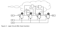
- FIG. 2 Logic Circuit After Scan Insertion, notice that each flip-flop has two input paths as controlled by a multiplexor on the input.
- the scan enable “SE” When the scan enable “SE” is asserted, the scan chain operates as a shift register. This allows for each flip-flop to be set to a specific state. It also allows for the observation of each flip-flop state as the values are shifted out of the device onto the scan output “SO”.
- SE scan enable
- the ‘and’ gate can be tested by shifting data into scan cells 3 and 2.
- the scan enable is de-asserted and a clock can be applied to capture the output of the combinational logic as observed at scan cell 1.
- the scan enable is once more applied and the result data as captured at scan cell 1 can be shifted through the scan chain until it can be seen on the device output for the scan chain.
- ac-scan The principles of ac-scan are very similar to that of scan. The major difference is that the clock that captures the output of the combinational logic into the observation scan cell is timed to the clock that placed the test condition at the input of the combinational logic. For example, if the spacing between the assertions of the two clocks is 1 ns, the test frequency is 1 GHz.
- Test patterns can be generated to check the speed of each of these paths for this design. However, with the magnitude of typical designs today, it is impossible to test all paths individually.
- testers apply a set of simulated stimulus, and validate that the response on the device outputs match the results expected from the simulation.
- Functional testers are designed to report in a go/no-go fashion that all of the outputs matched the expected results for all checked strobe points or not.
- Functional testers are not architected to understand design criteria of the device under test such as the scan structures. Thus, while testers can understand which output signals contained failures, each output signal can represent tens of thousands of internal scan cells.
- a method to associate fail data measured on a tester with the structural, logical, and physical context and performance metric enabling a rapid analysis and understanding of possible clusters of failure that stem from a common design or manufacturing origin; a way to select from huge volumes of test data the information to analyze patterns in defects that result in failures at or above certain speeds of operation; a way to view failures in different contextual backgrounds to determine commonality among failures that may reveal a addressable cause; a way to compress data without losing essential details for analysis in a reasonable and economic time; a way to present data for analysis that can be more easily understood and communicated; and a method of tracing the envelope of failures as a test parameter is swept through a range of values.
- Real-Time Mapping of Pattern Strobes to Scan Cells is accomplished through a software architecture that can associate each strobe point with an internal scan cell.
- the controlling software process knows the associated scan cell.
- the test pattern controlling software has the method of creating a look-up table of each and every “Load-Capture-Unload” operation, also known as a scan pattern, contained in the test pattern set. By recording the start of the unload operation for each scan pattern, and recognizing that all scan chains will unload at the same time, the tester cycle offset from the closest previous unload point prior to a given failure will determine the scan cell position within the chain. The chain is determined by the output signal of the device.
- the present invention enables datalogging from inside the device, yielding timing performance information about the logic behind each and every flip-flop in the scan chain. It is understood that a scan cell in a scan chain is represented by a bit position in an array of bits.
- the present invention further comprises the step of
- Reporting a timing measurement comprises at least one of:
- the method further comprises associating all test failures to scan cells in a scan chain in real time and updating the per scan cell results for each timing increment.
- the present invention may be tangibly embodied as an article of manufacture comprising: a computer readable media comprising a data structure, wherein said data structure comprises a representation of a timing measurement for a plurality of scan cells, wherein said plurality comprises two or more scan cells of a scan chain.
- FIG. 1 Schematic of a logic circuit prior to scan insertion
- FIG. 2 Schematic of a logic circuit after scan insertion
- FIG. 3 AC-Scan Timing Diagram of “Load-Capture-Unload”
- FIG. 4 Multiple Scan Patterns and Chains Timing Diagram
- FIG. 5 Flowchart of Frequency Scan Software Process
- FIG. 6 Embodiment Control of capturing failures by selecting test points
- FIG. 7 Embodiment displaying failures in cells in chains at test point
- FIG. 8 Embodiment displaying failures in histogram view
- FIG. 9 Embodiment displaying failures in hierarchy at certain test point
- FIG. 4 Multiple Scan Patterns and Chains shows the timing diagram for a test pattern set with four scan patterns, three scan chains, and four scan cells per each chain to illustrate the multiple dimensions. In this example, 48 total strobes are shown for 12 scan cells. For each scan chain, there is a scan output signal. Each scan cell must be stitched into a scan chain.
- scan cells may include millions of scan cells. These scan cells are distributed amongst a number of scan chains that may range from a handful to hundreds. Thus, scan chains may contain hundreds of scan cells to tens of thousands. For example, if a device contains 1 million scan cells and 100 scan chains, each scan chain would contain about 10,000 scan cells. The exact number of scan cells in each scan chain is determined by the chip designer. However, the designer usually strives to have balanced scan chains for optimum test time performance.
- each scan cell is typically strobed per scan pattern.
- the test pattern set contained 10,000 scan patterns for a design that contained 1 million scan cells, there would be a total 10 billion strobes to map to these 1 million scan cells.
- the technique for mapping the passes and fails of strobe points to scan cells is to index each strobe point by scan output signal, thus identifying the scan chain.
- the software keeps a map of the start of the unload operation for each scan pattern by tester cycle count. Thus, when a fail is encountered, the tester cycle count can be referenced against the unload marker to determine the bit position within the chain.
- SpeedScan significantly simplifies the complex process of retrieving the timing performance behind every flip-flop using a single easy to use form.
- the user selects whether the characterization is to be performed in the time or frequency domain and the Start and Stop parameters.
- the Launch and Capture clock attributes are selected from drop-down menus populated from Pattern Exec context.
- SpeedScan can be invoked from a graphical tool, or from a run-time test program call.
- the invention further comprises calculating the necessary timing values for each step of the sweep, and applying them to hardware.
- Conventional wafer level data analysis tools do not have the ability to respond to test programs and in turn control the values applied to test equipment in real time.
- data logging mechanics track results on a flip-flop basis, even for designs with millions of flip-flops, displaying progress with a color spectrum of the number of failing flip-flops at each test point on the sweep.
- the Care filter can be used to reduce the collected data to specific scan chains of interest. Select specific design elements for display with clearly labeled tree menus.
- SpeedMap expands failure analysis capabilities to include speed characterization data.
- the invention comprises the method of simultaneously displaying at least two of a structural view, a hierarchical view, and a histogram view.
- Structural test results generate complete pattern, chain, and bit information for better problem solving and fast debug. Users can dial a frequency to get a color spectrum display for each flip-flop as they are stitched into their scan chain.
- the Fail contrast slider controls the resolution of the fail density.
- the Speed contrast slider controls the failure frequency display.
- the “Hierarchical View” mode allows users to view failures by functional behavioral blocks—start from a core level and zoom down to the lowest-level design module.
- frequency performance can be observed by filtered circuit.
- the present invention comprises innovations in three areas, the testing of devices with scan chains and scan cells with pulse pairs along a spectrum of frequencies assigned to test points, the recording of the fastest pass or the slowest failure by scan cell in scan chain, logical hierarchy, and physical coordinates, and displaying the failure data as frequency is swept from slow to fast or fast to slow under user control.
- This is a method for improving the manufacturing yield of semiconductor devices at higher speeds.
- the first step is testing a logic device with an AC-Scan pattern at a plurality of testpoints, wherein a testpoint corresponds to a frequency rate of applying a launch-capture pair of clock pulses, and wherein an AC-Scan pattern is synthesized to exercise the flipflops in the critical paths which are most vulnerable to delay defects. While an enormous amount of data is available from this series of tests, it can be efficiently and economically stored as follows:
- a testpoint representing a frequency at which an AC scan test pattern causes a scan cell to fail
- a testpoint representing the highest frequency at which an AC scan test pattern causes a scan cell to pass
- an identifier of the scan test pattern which causes the scan cell to fail an identifier of the position of the scan cell in a scan chain, an identifier of a scan chain in a die, an identifier of a unique die in a wafer, an identifier of a wafer, a hierarchical design name for a failing scan cell consistent with the design database, a physical coordinate of the position of the scan cell in a die, a physical coordinate of the position of the die in a wafer, and a notation in the event that the scan cell has never passed or never failed any of the tests at any of the test points.
- the engineer seeking to analyze and cure speed related defects may then visualize the database of failures/frequency by displaying on a graphical computer display at least three of: a movable graphical icon by mouse or keyboard selecting a testpoint on a continuum of frequencies at which speed sensitive test patterns have been applied to the device; a failing scan cell in a scan chain in an array of scan cells in scan chains, said failing scan cell presenting test values inconsistent with expected test values for an AC-Scan test pattern and at least one frequency corresponding to a testpoint; a failing scan cell in a hierarchical list of flip-flops described in a design description language, said failing scan cell presented as one of a block diagram, a net list and an electrical schematic; a failing scan cell in a physical map of the device under test said failing scan cell presented in the context of other scan cells located in the same region of the device; a failing scan cell in a physical map of the wafer under test said failing scan cell presented in the context of other scan cells located in the same region of the wafer.
- the invention comprises a method comprising the following steps: collecting a plurality of test pattern failures; associating one of said plurality of test pattern failures to a scan cell; responsive to a first failure of the first testpoint, setting a scan cell record value in a results record to a frequency of a previous testpoint, displaying the failures in physical, logical, and scan cell order as the user selects a frequency along the continuum of testpoints.
Abstract
Description
-
- MUXD
- This scan flip-flop approach places a mux on the front end of the D-input. The selector to the mux, known as the scan enable, determines whether to use the mission mode input or the scan test input.
- LSSD
- Another common scan flip-flop approach is to use two clocks. One clock latches the mission path input into the flip-flop while the second clock latches the scan test input data into the flip-flop.
Scan Chains
- Another common scan flip-flop approach is to use two clocks. One clock latches the mission path input into the flip-flop while the second clock latches the scan test input data into the flip-flop.
- MUXD
-
- 1. From scan
cell 3 through the inverter intoscan cell 2 - 2. From scan
cell 3 through the ‘and’ gate intoscan cell 1 - 3. From scan
cell 2 through the ‘and’ gate intoscan cell 1 - 4. From scan
cell 3 through the ‘and’ gate, through the ‘or’ gate, intoscan cell 0 - 5. From scan
cell 2 through the ‘and’ gate, through the ‘or’ gate, intoscan cell 0 - 6. From
scan cell 1 through the ‘or’ gate intoscan cell 0
- 1. From scan
-
- At the start of the frequency sweep, the software will create a results record with an entry per each scan cell in the device design. This record will be initialized with an unmeasured “PASS” result per each scan cell.
-
- The frequency sweep will define a number of frequency test points. For example, sweeping from 300 MHz to 400 MHz with 5 MHz resolution equates to 20 steps or 21 test points. In an embodiment, the process is described to execute the test points in order from the slowest frequency to the highest.
-
- For each test point, the timing for the test frequency must be applied. The ac-scan frequency is determined by the proximity of the launch event to the capture event. Thus, whether the tester is driving a reference clock to a PLL, or driving the launch and capture clocks directly through one or more signals, this must be set according to the test point.
- If the tester is providing a reference clock to an internal PLL, the multiplication ratio for the PLL must be provided. For example, if the test point is 3.2 GHz, and the multiplication ratio is 32, the reference clock to the PLL must be set to 100 MHz.
- If the tester is providing the launch and capture clocks directly, the position of the capture clock relative to the launch clock must be adjusted. This may require adjustment of the launch clock pulse width. For example, consider default timing for test patterns at 50 MHz launch/capture with 5 ns pulse widths. To change the timing to achieve a 200 MHz test point, the leading edge of the capture clock must be adjusted to 5 ns after the leading edge of the launch clock. This would be at the same point of the trailing edge of the launch clock unless the pulse width of the launch clock is adjusted as well. The process defines the relative placement of the trailing to leading edge of the launch clock at min(1/(freq*2), original p/w).
-
- After the timing is set for each test point, the pattern is executed and all failures are collected and mapped to scan cells.
-
- These failures collected at each test point will be used to update the results record. If the failure is the first for a scan cell, the scan cell result will be set to the frequency of the previous test point. If this is the first test point, the result will be set to “FAIL”.
- If the failure is not the first for a scan cell, it will be ignored.
- These failures collected at each test point will be used to update the results record. If the failure is the first for a scan cell, the scan cell result will be set to the frequency of the previous test point. If this is the first test point, the result will be set to “FAIL”.
-
- Any scan cell that does not encounter a strobe failure will be left with the a marker in the results record indicating that either the patterns did not test this cell, or the test points did not exercise a frequency fast enough to induce a failure.
Claims (12)
Priority Applications (1)
| Application Number | Priority Date | Filing Date | Title |
|---|---|---|---|
| US11/563,612 US8006149B2 (en) | 2006-11-27 | 2006-11-27 | System and method for device performance characterization in physical and logical domains with AC SCAN testing |
Applications Claiming Priority (1)
| Application Number | Priority Date | Filing Date | Title |
|---|---|---|---|
| US11/563,612 US8006149B2 (en) | 2006-11-27 | 2006-11-27 | System and method for device performance characterization in physical and logical domains with AC SCAN testing |
Publications (2)
| Publication Number | Publication Date |
|---|---|
| US20080126896A1 US20080126896A1 (en) | 2008-05-29 |
| US8006149B2 true US8006149B2 (en) | 2011-08-23 |
Family
ID=39495697
Family Applications (1)
| Application Number | Title | Priority Date | Filing Date |
|---|---|---|---|
| US11/563,612 Expired - Fee Related US8006149B2 (en) | 2006-11-27 | 2006-11-27 | System and method for device performance characterization in physical and logical domains with AC SCAN testing |
Country Status (1)
| Country | Link |
|---|---|
| US (1) | US8006149B2 (en) |
Cited By (2)
| Publication number | Priority date | Publication date | Assignee | Title |
|---|---|---|---|---|
| US20140223389A1 (en) * | 2013-02-01 | 2014-08-07 | Qualcomm Incorporated | System and method to design and test a yield sensitive circuit |
| US20150168491A1 (en) * | 2013-12-16 | 2015-06-18 | International Business Machines Corporation | Collecting diagnostic data from chips |
Families Citing this family (2)
| Publication number | Priority date | Publication date | Assignee | Title |
|---|---|---|---|---|
| JP6381409B2 (en) * | 2014-10-30 | 2018-08-29 | ルネサスエレクトロニクス株式会社 | Failure diagnosis system, failure diagnosis method and failure diagnosis program |
| US10866753B2 (en) * | 2018-04-03 | 2020-12-15 | Xilinx, Inc. | Data processing engine arrangement in a device |
Citations (11)
| Publication number | Priority date | Publication date | Assignee | Title |
|---|---|---|---|---|
| JPH0651031A (en) * | 1992-08-04 | 1994-02-25 | Matsushita Electric Ind Co Ltd | Semiconductor test circuit |
| US6061813A (en) * | 1996-12-19 | 2000-05-09 | Advantest Corporation | Memory test set |
| US6278956B1 (en) * | 1998-04-30 | 2001-08-21 | International Business Machines Corporation | Method of locating a failed latch in a defective shift register |
| US20020129310A1 (en) * | 2001-03-12 | 2002-09-12 | Samsung Electronics Co., Ltd. | Semiconductor integrated circuit with local monitor circuits |
| US20050222795A1 (en) * | 2004-04-06 | 2005-10-06 | Rodgers Richard S | Apparatus and method for compensating clock period elongation during scan testing in an integrated circuit (IC) |
| US20060111873A1 (en) * | 2004-03-31 | 2006-05-25 | Yu Huang | Compactor independent direct diagnosis of test hardware |
| US7058869B2 (en) * | 2003-01-28 | 2006-06-06 | Syntest Technologies, Inc. | Method and apparatus for debug, diagnosis, and yield improvement of scan-based integrated circuits |
| US20060242473A1 (en) * | 2005-04-07 | 2006-10-26 | Wahl Mark A | Phase optimization for data communication between plesiochronous time domains |
| US7292720B2 (en) * | 2002-07-09 | 2007-11-06 | Siemens Aktiengesellschaft | Method and magnetic resonance tomography apparatus for graphic planning of angiographic exposures using a contrast agent |
| US7313746B2 (en) * | 2005-09-30 | 2007-12-25 | Nec Laboratories America, Inc. | Test output compaction for responses with unknown values |
| US7516379B2 (en) * | 2004-04-06 | 2009-04-07 | Avago Technologies General Ip (Singapore) Pte. Ltd. | Circuit and method for comparing circuit performance between functional and AC scan testing in an integrated circuit (IC) |
-
2006
- 2006-11-27 US US11/563,612 patent/US8006149B2/en not_active Expired - Fee Related
Patent Citations (11)
| Publication number | Priority date | Publication date | Assignee | Title |
|---|---|---|---|---|
| JPH0651031A (en) * | 1992-08-04 | 1994-02-25 | Matsushita Electric Ind Co Ltd | Semiconductor test circuit |
| US6061813A (en) * | 1996-12-19 | 2000-05-09 | Advantest Corporation | Memory test set |
| US6278956B1 (en) * | 1998-04-30 | 2001-08-21 | International Business Machines Corporation | Method of locating a failed latch in a defective shift register |
| US20020129310A1 (en) * | 2001-03-12 | 2002-09-12 | Samsung Electronics Co., Ltd. | Semiconductor integrated circuit with local monitor circuits |
| US7292720B2 (en) * | 2002-07-09 | 2007-11-06 | Siemens Aktiengesellschaft | Method and magnetic resonance tomography apparatus for graphic planning of angiographic exposures using a contrast agent |
| US7058869B2 (en) * | 2003-01-28 | 2006-06-06 | Syntest Technologies, Inc. | Method and apparatus for debug, diagnosis, and yield improvement of scan-based integrated circuits |
| US20060111873A1 (en) * | 2004-03-31 | 2006-05-25 | Yu Huang | Compactor independent direct diagnosis of test hardware |
| US20050222795A1 (en) * | 2004-04-06 | 2005-10-06 | Rodgers Richard S | Apparatus and method for compensating clock period elongation during scan testing in an integrated circuit (IC) |
| US7516379B2 (en) * | 2004-04-06 | 2009-04-07 | Avago Technologies General Ip (Singapore) Pte. Ltd. | Circuit and method for comparing circuit performance between functional and AC scan testing in an integrated circuit (IC) |
| US20060242473A1 (en) * | 2005-04-07 | 2006-10-26 | Wahl Mark A | Phase optimization for data communication between plesiochronous time domains |
| US7313746B2 (en) * | 2005-09-30 | 2007-12-25 | Nec Laboratories America, Inc. | Test output compaction for responses with unknown values |
Cited By (5)
| Publication number | Priority date | Publication date | Assignee | Title |
|---|---|---|---|---|
| US20140223389A1 (en) * | 2013-02-01 | 2014-08-07 | Qualcomm Incorporated | System and method to design and test a yield sensitive circuit |
| US9081932B2 (en) * | 2013-02-01 | 2015-07-14 | Qualcomm Incorporated | System and method to design and test a yield sensitive circuit |
| US20150168491A1 (en) * | 2013-12-16 | 2015-06-18 | International Business Machines Corporation | Collecting diagnostic data from chips |
| US9372232B2 (en) * | 2013-12-16 | 2016-06-21 | International Business Machines Corporation | Collecting diagnostic data from chips |
| US9746516B2 (en) | 2013-12-16 | 2017-08-29 | International Business Machines Corporation | Collecting diagnostic data from chips |
Also Published As
| Publication number | Publication date |
|---|---|
| US20080126896A1 (en) | 2008-05-29 |
Similar Documents
| Publication | Publication Date | Title |
|---|---|---|
| US6141790A (en) | Instructions signature and primary input and primary output extraction within an IEEE 1149.1 compliance checker | |
| US8280687B2 (en) | Direct fault diagnostics using per-pattern compactor signatures | |
| US6012155A (en) | Method and system for performing automatic extraction and compliance checking of an IEEE 1149.1 standard design within a netlist | |
| US7870519B2 (en) | Method for determining features associated with fails of integrated circuits | |
| US7225374B2 (en) | ABIST-assisted detection of scan chain defects | |
| US7568139B2 (en) | Process for identifying the location of a break in a scan chain in real time | |
| US7124342B2 (en) | Smart capture for ATPG (automatic test pattern generation) and fault simulation of scan-based integrated circuits | |
| CN106291324A (en) | On a kind of sheet being applicable to high speed integrated circuit, differential delay is measured system and reclaims integrated circuit recognition methods | |
| US20180252768A1 (en) | Test Application Time Reduction Using Capture-Per-Cycle Test Points | |
| US6970815B1 (en) | Method of discriminating between different types of scan failures, computer readable code to cause a display to graphically depict one or more simulated scan output data sets versus time and a computer implemented circuit simulation and fault detection system | |
| CN109725248A (en) | A kind of the on piece detection system and test method of identification aging recycling integrated circuit | |
| US8006149B2 (en) | System and method for device performance characterization in physical and logical domains with AC SCAN testing | |
| CN110347595A (en) | A kind of FPGA internal resource is screened and localization method and system | |
| Appello et al. | Understanding yield losses in logic circuits | |
| US9310431B2 (en) | Diagnosis framework to shorten yield learning cycles of advanced processes | |
| Guo et al. | Detection and diagnosis of static scan cell internal defect | |
| Nelson et al. | Extracting defect density and size distributions from product ICs | |
| US11379644B1 (en) | IC chip test engine | |
| US6775798B2 (en) | Fast sampling test bench | |
| US7188043B1 (en) | Boundary scan analysis | |
| Auvray et al. | Evolution of navigation and simulation tools in failure analysis | |
| US20170010320A1 (en) | Reducing test time and system-on-chip (soc) area reduction using simultaneous clock capture based on voltage sensor input | |
| Nandakumar et al. | High Throughput Multiple Device Chain Diagnosis Methodology for Clock and Control Line Defects | |
| GOPIKRISHNA | Performance Analysis of Design for Testability with EDT and without EDT Architecture | |
| Khalil et al. | Design for testability of circuits and Systems; An overview |
Legal Events
| Date | Code | Title | Description |
|---|---|---|---|
| AS | Assignment |
Owner name: CA UGMA, UNTIL THE AGE OF 21 FOR CLAYTON JAMES MUR Free format text: GRANT OF PATENT SECURITY INTEREST;ASSIGNOR:INOVYS CORPORATION;REEL/FRAME:019617/0445 Effective date: 20070425 Owner name: BURLISON, CUST. UGMA, UNTIL THE AGE OF 21, FBO AMA Free format text: GRANT OF PATENT SECURITY INTEREST;ASSIGNOR:INOVYS CORPORATION;REEL/FRAME:019617/0445 Effective date: 20070425 Owner name: LANDINGS INVESTMENT PARTNERS, LLC, CALIFORNIA Free format text: GRANT OF PATENT SECURITY INTEREST;ASSIGNOR:INOVYS CORPORATION;REEL/FRAME:019617/0445 Effective date: 20070425 Owner name: CA UGMA, UNTIL THE AGE OF 21 FOR CHRISTIAN PHILLIP Free format text: GRANT OF PATENT SECURITY INTEREST;ASSIGNOR:INOVYS CORPORATION;REEL/FRAME:019617/0445 Effective date: 20070425 Owner name: TECHFUND CAPITAL II, L.P., CALIFORNIA Free format text: GRANT OF PATENT SECURITY INTEREST;ASSIGNOR:INOVYS CORPORATION;REEL/FRAME:019617/0445 Effective date: 20070425 Owner name: ALL CHEMICAL DISPOSAL, INC., CALIFORNIA Free format text: GRANT OF PATENT SECURITY INTEREST;ASSIGNOR:INOVYS CORPORATION;REEL/FRAME:019617/0445 Effective date: 20070425 Owner name: MURABITO 1994 LIVING TRUST DATED JANUARY 11, 1994, Free format text: GRANT OF PATENT SECURITY INTEREST;ASSIGNOR:INOVYS CORPORATION;REEL/FRAME:019617/0445 Effective date: 20070425 Owner name: BURLISON, CUST. UGMA, UNTIL THE AGE OF 21, FBO COU Free format text: GRANT OF PATENT SECURITY INTEREST;ASSIGNOR:INOVYS CORPORATION;REEL/FRAME:019617/0445 Effective date: 20070425 Owner name: BURLISON, CUST. UGMA, UNTIL THE AGE OF 21, FBO ALF Free format text: GRANT OF PATENT SECURITY INTEREST;ASSIGNOR:INOVYS CORPORATION;REEL/FRAME:019617/0445 Effective date: 20070425 Owner name: BURLISON, CUST. UGMA, UNTIL THE AGE OF 21, FBO JOS Free format text: GRANT OF PATENT SECURITY INTEREST;ASSIGNOR:INOVYS CORPORATION;REEL/FRAME:019617/0445 Effective date: 20070425 Owner name: BURLISON, CUST. UGMA, UNTIL THE AGE OF 21, FBO CHR Free format text: GRANT OF PATENT SECURITY INTEREST;ASSIGNOR:INOVYS CORPORATION;REEL/FRAME:019617/0445 Effective date: 20070425 Owner name: CA UGMA, UNTIL THE AGE OF 21 FOR JOSEPH ANTHONY MU Free format text: GRANT OF PATENT SECURITY INTEREST;ASSIGNOR:INOVYS CORPORATION;REEL/FRAME:019617/0445 Effective date: 20070425 Owner name: STORM VENTURES FUND II, LLC, CALIFORNIA Free format text: GRANT OF PATENT SECURITY INTEREST;ASSIGNOR:INOVYS CORPORATION;REEL/FRAME:019617/0445 Effective date: 20070425 Owner name: SYNOPSYS, INC., CALIFORNIA Free format text: GRANT OF PATENT SECURITY INTEREST;ASSIGNOR:INOVYS CORPORATION;REEL/FRAME:019617/0445 Effective date: 20070425 Owner name: TECHFARM VENTURES, L.P., CALIFORNIA Free format text: GRANT OF PATENT SECURITY INTEREST;ASSIGNOR:INOVYS CORPORATION;REEL/FRAME:019617/0445 Effective date: 20070425 Owner name: BUCKINGHAM T.I.C., JAMES R. AND LINDA L., TEXAS Free format text: GRANT OF PATENT SECURITY INTEREST;ASSIGNOR:INOVYS CORPORATION;REEL/FRAME:019617/0445 Effective date: 20070425 Owner name: CA UGMA, UNTIL THE AGE OF 21 FOR AMANDA TAYLOR MUR Free format text: GRANT OF PATENT SECURITY INTEREST;ASSIGNOR:INOVYS CORPORATION;REEL/FRAME:019617/0445 Effective date: 20070425 Owner name: QUACH, PHUONG, CALIFORNIA Free format text: GRANT OF PATENT SECURITY INTEREST;ASSIGNOR:INOVYS CORPORATION;REEL/FRAME:019617/0445 Effective date: 20070425 Owner name: HARTWIG FAMILY TRUST, LINDA, CALIFORNIA Free format text: GRANT OF PATENT SECURITY INTEREST;ASSIGNOR:INOVYS CORPORATION;REEL/FRAME:019617/0445 Effective date: 20070425 Owner name: CA UGMA, UNTIL THE AGE OF 21 FOR COURTNEY MICHELLE Free format text: GRANT OF PATENT SECURITY INTEREST;ASSIGNOR:INOVYS CORPORATION;REEL/FRAME:019617/0445 Effective date: 20070425 Owner name: MURABITO TTEE MURABITO 1994 LIVING TRUST, UA DTD 0 Free format text: GRANT OF PATENT SECURITY INTEREST;ASSIGNOR:INOVYS CORPORATION;REEL/FRAME:019617/0445 Effective date: 20070425 Owner name: ALL CHEMICAL DISPOSAL, INC. 401(K) PROFIT SHARING Free format text: GRANT OF PATENT SECURITY INTEREST;ASSIGNOR:INOVYS CORPORATION;REEL/FRAME:019617/0445 Effective date: 20070425 Owner name: CA UGMA, UNTIL THE AGE OF 21 FOR ALFRED CHARLES MU Free format text: GRANT OF PATENT SECURITY INTEREST;ASSIGNOR:INOVYS CORPORATION;REEL/FRAME:019617/0445 Effective date: 20070425 Owner name: STORM VENTURES FUND II(A), LLC, CALIFORNIA Free format text: GRANT OF PATENT SECURITY INTEREST;ASSIGNOR:INOVYS CORPORATION;REEL/FRAME:019617/0445 Effective date: 20070425 Owner name: PALOMAR VENTURES II, L.P., CALIFORNIA Free format text: GRANT OF PATENT SECURITY INTEREST;ASSIGNOR:INOVYS CORPORATION;REEL/FRAME:019617/0445 Effective date: 20070425 Owner name: SOHAIL, FAYSAL, CALIFORNIA Free format text: GRANT OF PATENT SECURITY INTEREST;ASSIGNOR:INOVYS CORPORATION;REEL/FRAME:019617/0445 Effective date: 20070425 Owner name: H.I.G. INOVYS, INC., FLORIDA Free format text: GRANT OF PATENT SECURITY INTEREST;ASSIGNOR:INOVYS CORPORATION;REEL/FRAME:019617/0445 Effective date: 20070425 Owner name: MORIHIRO, KOJI, JAPAN Free format text: GRANT OF PATENT SECURITY INTEREST;ASSIGNOR:INOVYS CORPORATION;REEL/FRAME:019617/0445 Effective date: 20070425 Owner name: CMEA VENTURES INFORMATION TECHNOLOGY II, CIVIL LAW Free format text: GRANT OF PATENT SECURITY INTEREST;ASSIGNOR:INOVYS CORPORATION;REEL/FRAME:019617/0445 Effective date: 20070425 Owner name: HUITUNG INVESTMENTS (BVI) LIMITED, CALIFORNIA Free format text: GRANT OF PATENT SECURITY INTEREST;ASSIGNOR:INOVYS CORPORATION;REEL/FRAME:019617/0445 Effective date: 20070425 Owner name: CMEA VENTURES INFORMATION TECHNOLOGY II, L.P., CAL Free format text: GRANT OF PATENT SECURITY INTEREST;ASSIGNOR:INOVYS CORPORATION;REEL/FRAME:019617/0445 Effective date: 20070425 Owner name: SHENGTUNG VENTURE CAPITAL CORPORATION, CALIFORNIA Free format text: GRANT OF PATENT SECURITY INTEREST;ASSIGNOR:INOVYS CORPORATION;REEL/FRAME:019617/0445 Effective date: 20070425 Owner name: CA UGMA, UNTIL THE AGE OF 21 FOR MARCUS PAUL MURAB Free format text: GRANT OF PATENT SECURITY INTEREST;ASSIGNOR:INOVYS CORPORATION;REEL/FRAME:019617/0445 Effective date: 20070425 Owner name: LAZAROW, WARREN T., CALIFORNIA Free format text: GRANT OF PATENT SECURITY INTEREST;ASSIGNOR:INOVYS CORPORATION;REEL/FRAME:019617/0445 Effective date: 20070425 Owner name: LAZAROW, TRUSTEES OF THE LAZAROW FAMILY TRUST, DAT Free format text: GRANT OF PATENT SECURITY INTEREST;ASSIGNOR:INOVYS CORPORATION;REEL/FRAME:019617/0445 Effective date: 20070425 Owner name: HOLLIFIELD, TED, CALIFORNIA Free format text: GRANT OF PATENT SECURITY INTEREST;ASSIGNOR:INOVYS CORPORATION;REEL/FRAME:019617/0445 Effective date: 20070425 Owner name: CA UGMA, UNTIL THE AGE OF 21 FOR TIMOTHY JOHN MURA Free format text: GRANT OF PATENT SECURITY INTEREST;ASSIGNOR:INOVYS CORPORATION;REEL/FRAME:019617/0445 Effective date: 20070425 |
|
| AS | Assignment |
Owner name: INOVYS CORPORATION, CALIFORNIA Free format text: ASSIGNMENT OF ASSIGNORS INTEREST;ASSIGNORS:DOKKEN, RICHARD C.;CHAN, GERALD S.;BURLISON, PHILLIP D.;REEL/FRAME:022209/0715;SIGNING DATES FROM 20090115 TO 20090116 Owner name: INOVYS CORPORATION, CALIFORNIA Free format text: ASSIGNMENT OF ASSIGNORS INTEREST;ASSIGNORS:DOKKEN, RICHARD C.;CHAN, GERALD S.;BURLISON, PHILLIP D.;SIGNING DATES FROM 20090115 TO 20090116;REEL/FRAME:022209/0715 |
|
| AS | Assignment |
Owner name: INOVYS CORPORATION, CALIFORNIA Free format text: RELEASE BY SECURED PARTY;ASSIGNORS:STORM VENTURES FUND II(A), LLC;STORM VENTURES FUND II, LLC;CMEA VENTURES INFORMATION TECHNOLOGY II, CIVIL LAW PARTNERSHIP;AND OTHERS;REEL/FRAME:023292/0417 Effective date: 20071231 |
|
| AS | Assignment |
Owner name: VERIGY (SINGAPORE) PTE. LTD., SINGAPORE Free format text: ASSIGNMENT OF ASSIGNORS INTEREST;ASSIGNOR:INOVYS CORPORATION;REEL/FRAME:023330/0760 Effective date: 20091006 Owner name: VERIGY (SINGAPORE) PTE. LTD.,SINGAPORE Free format text: ASSIGNMENT OF ASSIGNORS INTEREST;ASSIGNOR:INOVYS CORPORATION;REEL/FRAME:023330/0760 Effective date: 20091006 |
|
| FEPP | Fee payment procedure |
Free format text: PAYOR NUMBER ASSIGNED (ORIGINAL EVENT CODE: ASPN); ENTITY STATUS OF PATENT OWNER: LARGE ENTITY |
|
| STCF | Information on status: patent grant |
Free format text: PATENTED CASE |
|
| AS | Assignment |
Owner name: ADVANTEST (SINGAPORE) PTE LTD, SINGAPORE Free format text: ASSIGNMENT OF ASSIGNORS INTEREST;ASSIGNOR:VERIGY (SINGAPORE) PTE LTD;REEL/FRAME:027896/0018 Effective date: 20120302 |
|
| FPAY | Fee payment |
Year of fee payment: 4 |
|
| AS | Assignment |
Owner name: ADVANTEST CORPORATION, JAPAN Free format text: ASSIGNMENT OF ASSIGNORS INTEREST;ASSIGNOR:ADVANTEST (SINGAPORE) PTE. LTD.;REEL/FRAME:035371/0265 Effective date: 20150401 |
|
| AS | Assignment |
Owner name: ADVANTEST CORPORATION, JAPAN Free format text: CORRECTIVE ASSIGNMENT TO CORRECT THE ASSIGNEE ADDRESS PREVIOUSLY RECORDED AT REEL: 035371 FRAME: 0265. ASSIGNOR(S) HEREBY CONFIRMS THE ASSIGNMENT;ASSIGNOR:ADVANTEST (SINGAPORE) PTE. LTD.;REEL/FRAME:035425/0768 Effective date: 20150401 |
|
| FEPP | Fee payment procedure |
Free format text: MAINTENANCE FEE REMINDER MAILED (ORIGINAL EVENT CODE: REM.); ENTITY STATUS OF PATENT OWNER: LARGE ENTITY |
|
| LAPS | Lapse for failure to pay maintenance fees |
Free format text: PATENT EXPIRED FOR FAILURE TO PAY MAINTENANCE FEES (ORIGINAL EVENT CODE: EXP.); ENTITY STATUS OF PATENT OWNER: LARGE ENTITY |
|
| STCH | Information on status: patent discontinuation |
Free format text: PATENT EXPIRED DUE TO NONPAYMENT OF MAINTENANCE FEES UNDER 37 CFR 1.362 |
|
| FP | Lapsed due to failure to pay maintenance fee |
Effective date: 20190823 |