US7956916B2 - Solid-state imaging device - Google Patents
Solid-state imaging device Download PDFInfo
- Publication number
- US7956916B2 US7956916B2 US12/195,584 US19558408A US7956916B2 US 7956916 B2 US7956916 B2 US 7956916B2 US 19558408 A US19558408 A US 19558408A US 7956916 B2 US7956916 B2 US 7956916B2
- Authority
- US
- United States
- Prior art keywords
- voltage
- unit
- charge
- optical signal
- state imaging
- Prior art date
- Legal status (The legal status is an assumption and is not a legal conclusion. Google has not performed a legal analysis and makes no representation as to the accuracy of the status listed.)
- Active, expires
Links
Images


Classifications
-
- H—ELECTRICITY
- H04—ELECTRIC COMMUNICATION TECHNIQUE
- H04N—PICTORIAL COMMUNICATION, e.g. TELEVISION
- H04N25/00—Circuitry of solid-state image sensors [SSIS]; Control thereof
- H04N25/70—SSIS architectures; Circuits associated therewith
- H04N25/76—Addressed sensors, e.g. MOS or CMOS sensors
- H04N25/77—Pixel circuitry, e.g. memories, A/D converters, pixel amplifiers, shared circuits or shared components
- H04N25/771—Pixel circuitry, e.g. memories, A/D converters, pixel amplifiers, shared circuits or shared components comprising storage means other than floating diffusion
-
- H—ELECTRICITY
- H04—ELECTRIC COMMUNICATION TECHNIQUE
- H04N—PICTORIAL COMMUNICATION, e.g. TELEVISION
- H04N25/00—Circuitry of solid-state image sensors [SSIS]; Control thereof
- H04N25/50—Control of the SSIS exposure
- H04N25/57—Control of the dynamic range
- H04N25/58—Control of the dynamic range involving two or more exposures
- H04N25/587—Control of the dynamic range involving two or more exposures acquired sequentially, e.g. using the combination of odd and even image fields
- H04N25/589—Control of the dynamic range involving two or more exposures acquired sequentially, e.g. using the combination of odd and even image fields with different integration times, e.g. short and long exposures
-
- H—ELECTRICITY
- H04—ELECTRIC COMMUNICATION TECHNIQUE
- H04N—PICTORIAL COMMUNICATION, e.g. TELEVISION
- H04N25/00—Circuitry of solid-state image sensors [SSIS]; Control thereof
- H04N25/50—Control of the SSIS exposure
- H04N25/57—Control of the dynamic range
- H04N25/59—Control of the dynamic range by controlling the amount of charge storable in the pixel, e.g. modification of the charge conversion ratio of the floating node capacitance
-
- H—ELECTRICITY
- H04—ELECTRIC COMMUNICATION TECHNIQUE
- H04N—PICTORIAL COMMUNICATION, e.g. TELEVISION
- H04N25/00—Circuitry of solid-state image sensors [SSIS]; Control thereof
- H04N25/70—SSIS architectures; Circuits associated therewith
- H04N25/76—Addressed sensors, e.g. MOS or CMOS sensors
- H04N25/77—Pixel circuitry, e.g. memories, A/D converters, pixel amplifiers, shared circuits or shared components
Definitions
- the present invention relates to a solid-state imaging device, and more particularly to a solid-state imaging device to be applied to a digital camera.
- a dynamic range of solid-state imaging devices has been approximately between 60 dB and 80 dB.
- the dynamic range is desired to be from 100 dB to 120 dB that is equivalent to visibility of the naked eye or a dynamic range of a silver salt film, or is desired to be improved to a much higher range for use in high-performance cameras, such as a vehicle-mounted camera and a monitoring camera.
- Patent Reference 1 Japanese Unexamined Patent Application Publication No. 2004-363666 discloses a technique of capturing frames each having a different exposure time in length, and combining the captured frames. Since a luminance range to be captured for one frame varies depending on a length of an exposure time, the dynamic range may be expanded by combining frames each having a different luminance range due to a different exposure time.
- FIG. 1 illustrates a schematic view of a solid-state imaging device of Patent Reference 1.
- the solid-state imaging device includes pixel units 171 , photodiodes 172 , noise cancellers 173 , and an amplifier 174 .
- the photodiode 172 is a light-receiving element.
- a timing controller in the drawing controls the constituent elements included in the solid-state imaging device, and causes the constituent elements to select a pixel row and a pixel column to be operated.
- a voltage level of a terminal Ri is set to be high according to an instruction of the timing controller, a cathode of the photodiode 172 is set to a higher voltage value (initial value).
- i is a natural number ranging from 1 to N.
- the solid-state imaging device is shifted to a charge integration mode that lowers a cathode potential according to light entering the photodiode 172 .
- the cathode potential of the photodiode 172 is outputted to an output terminal through the noise canceller 173 and the amplifier 174 .
- a cathode of the photodiode 172 is set to a higher voltage value (initial value), and is shifted to a new charge integration mode.
- FIG. 2 illustrates exposure times and output timings in the solid-state imaging device described in Patent Reference 1.
- the exposure time is divided into 3 categories, long (LAi), short (SAi), and very short (VSAi), and LRi, SRi, and VSRi represent timing when a signal obtained in a charge integration mode is outputted after the respective exposure times, where i is a natural number ranging from 1 to N. Since light is converted to a voltage according to an intensity of light, in other words, normal light during the LAi, strong light during the SAi, and very strong light during the VSAi, a wide dynamic range becomes possible with the solid-state imaging device.
- Patent Reference 1 since the technique of Patent Reference 1 needs to store signals separately, depending on respective exposure times, LAi, SAi, and VSAi, it takes long processing time. Furthermore, the solid-state imaging device is necessary to provide a storing unit that stores the signals, and a signal combining unit that combines signals, outside the solid-state imaging device to execute post-processing.
- the present invention has an object of combining signals for a short period of time in a solid-state imaging device without such a storing unit and a charge combining unit outside the solid-state imaging device to expand a dynamic range of the solid-state imaging device.
- the solid-state imaging device has pixel units that are two-dimensionally arranged, and includes: a light-receiving element that generates an optical signal charge corresponding to an intensity and an exposure time of light entering the light-receiving element; a transferring unit configured to transfer the optical signal charge; a charge combining unit configured to generate a signal voltage corresponding to the optical signal charge; a storing unit configured to store a signal voltage corresponding to the optical signal charge in the charge combining unit; and a voltage setting unit configured to set a value of a voltage in the charge combining unit to a value corresponding to the signal voltage stored by the storing unit.
- an optical signal charge can be transferred sequentially for a plurality of times without any influence of voltage level variation in a pixel according to the passage of time. Furthermore, a charge combining unit is not necessary outside a solid-state imaging device, thus expanding a dynamic range obtained by combining optical signal charges for a short period of time in a solid-state imaging device.
- each of the pixel units preferably includes the light-receiving element, the transferring unit, the charge combining unit, the storing unit, and the voltage setting unit.
- an optical signal charge can be transferred sequentially for a plurality of times without any influence of voltage level variation in a pixel according to the passage of time. Furthermore, a charge combining unit is not necessary outside a solid-state imaging device, thus combining optical signal charges for a short period of time in a solid-state imaging device.
- the charge combining unit may include: an accumulating unit configured to accumulate the optical signal charge; a reset unit configured to reset a voltage in the accumulating unit; and a difference circuit unit configured to output a voltage obtained by combining, with a predetermined reference voltage, a difference voltage between a voltage obtained by resetting the voltage in the accumulating unit and the signal voltage corresponding to the optical signal charge accumulated by the accumulating unit, and the voltage setting unit may set the signal voltage stored by the storing unit as the reference voltage of the difference circuit unit.
- optical signal charges can be combined with fewer functional variations in pixels, because an optical signal voltage corresponding to an optical signal charge generated in a light-receiving element is added to a voltage obtained as a difference between the reset output voltage and the combined signal output voltage all the time.
- each of the pixel units may include the light-receiving element, the transferring unit, the accumulating unit, and the reset unit, and the difference circuit unit, the storing unit, and the voltage setting unit are formed for each column signal line connected to a portion of the pixel units that are arranged in an identical column.
- the number of circuit elements and an area for each solid-state imaging device can be reduced, because the difference circuit unit, the storing unit, and the voltage setting unit are provided not for each pixel unit but for each column signal line.
- the voltage setting unit may include one of: a transistor including a gate terminal connected to the storing unit, a drain terminal connected to a power supply unit, and a source terminal connected to the charge combining unit through a switch; and a transistor including a gate terminal connected to the storing unit, a source terminal connected to a power supply unit, and a drain terminal connected to the charge combining unit through a switch.
- a voltage setting unit may be formed by simple circuit elements, a circuit scale of an entire solid-state imaging device is simplified.
- the voltage setting unit may include an output terminal that is connected to a column signal line common to a portion of the pixel units arranged in a column direction, and the output terminal may output the value corresponding to the signal voltage stored by the storing unit as a pixel signal.
- the voltage setting unit can amplify the voltage in the storing unit, and also functions as an output circuit.
- reduction in the number of circuit elements increases an area ratio (open area ratio) of a light-receiving element to a pixel, and improves a sensitivity of the pixel.
- an area ratio open area ratio
- the number of chips that can be placed on a semiconductor substrate may increase, thus reducing costs.
- the reset voltage applying circuit may be connected to an end of the column signal line, and apply a reset voltage to the charge combining unit and the storing unit through the output terminal.
- a reset circuit is not necessary in a pixel and a column signal line functions also as a wiring for applying a reset voltage, an area ratio (open area ratio) of a light-receiving element to a pixel increases, and a sensitivity of the pixel may be improved.
- an area ratio open area ratio
- the number of chips that can be placed on a semiconductor substrate may increase, thus reducing costs.
- the voltage setting unit may include a buffer circuit that inputs a voltage outputted from the storing unit.
- signal charges can be precisely combined by preventing a voltage from dropping due to a load in a circuit element included in the voltage setting unit and in a peripheral circuit.
- the storing unit may include: a first capacitor connected, through a switch, between an output terminal in the difference circuit unit and the charge combining unit; and a second capacitor connected between the output terminal and a ground, and the voltage setting unit may set, in the charge combining unit, a voltage held in the first capacitor.
- the voltage setting unit and the storing unit may be made up of less number of circuit elements. Furthermore, signal charges can be precisely combined through use of a capacitor, thus preventing a voltage from dropping due to a load in a circuit element included in the voltage setting unit itself and in a peripheral circuit.
- the storing unit may include a third capacitor having one terminal connected to the charge combining unit through a switch, and having the other terminal connected to a bias circuit.
- a voltage drop occurring in the voltage setting unit connected in a latter stage may be compensated by applying a bias voltage when a voltage is set in the voltage setting unit, thus enabling precise combination of signal charges.
- the present invention can be realized not only as a solid-state imaging device having the aforementioned characteristics but also as a solid-state imaging apparatus including such a solid-state imaging device that has the same structure and advantage as that of the solid-state imaging device.
- the present invention can be realized not only as the solid-state imaging device or the solid-state imaging apparatus that has the aforementioned characteristics but also as a camera that includes such a solid-state imaging device or the solid-state imaging apparatus having the same structure and advantage.
- the present invention can be realized not only as the solid-state imaging device or the solid-state imaging apparatus having such characteristic units therein but also as a driving method having the characteristic units of the solid-state imaging device or the solid-state imaging apparatus as steps.
- an optical signal charge can be transferred sequentially for a plurality of times, enabling combination of the charges in the solid-state imaging device for a short period of time.
- a dynamic range may be expanded without a charge combining unit outside the solid-state imaging device.
- FIG. 1 illustrates a schematic view of a solid-state imaging device of Patent Reference 1.
- FIG. 2 illustrates exposure times and output timings in the solid-state imaging device described in Patent Reference 1.
- FIG. 3 illustrates a configuration of a basic circuit of the solid-state imaging device according to the first embodiment of the present invention.
- FIG. 4 illustrates a configuration of a basic circuit of the solid-state imaging device according to the first embodiment of the present invention.
- FIG. 5 illustrates a configuration of the solid-state imaging device of the first variation according to the first embodiment of the present invention.
- FIG. 6 illustrates a configuration of the solid-state imaging device of the second variation according to the first embodiment of the present invention.
- FIG. 7 illustrates a drive timing chart of the solid-state imaging device of the first variation according to the first embodiment of the present invention.
- FIG. 8 illustrates a drive timing chart of the solid-state imaging device of the third variation according to the first embodiment of the present invention.
- FIG. 9 illustrates a functional configuration of a solid-state imaging apparatus including the solid-state imaging device according to the present invention.
- FIG. 10 illustrates a circuit configuration of the solid-state imaging device of the fourth variation according to the first embodiment of the present invention.
- FIG. 11 illustrates a drive timing chart of the solid-state imaging device of the fourth variation according to the first embodiment of the present invention.
- FIG. 12 illustrates a configuration of the solid-state imaging device of the fifth variation according to the first embodiment of the present invention.
- FIG. 13 illustrates a drive timing chart of the solid-state imaging device of the fifth variation according to the first embodiment of the present invention.
- FIG. 14A illustrates a configuration of the solid-state imaging device of the sixth variation according to the first embodiment of the present invention.
- FIG. 14B illustrates a configuration of a buffer circuit.
- FIG. 15 illustrates a drive timing chart of the solid-state imaging device of the sixth variation according to the first embodiment of the present invention.
- FIG. 16 illustrates a configuration of the solid-state imaging device of the seventh variation according to the first embodiment of the present invention.
- FIG. 17 illustrates a timing chart of the solid-state imaging device of the seventh variation according to the first embodiment of the present invention.
- FIG. 18A illustrates a functional block diagram of a solid-state imaging apparatus including the solid-state imaging device according to the first embodiment of the present invention.
- FIG. 18B illustrates a functional block diagram of a conventional solid-state imaging apparatus.
- FIG. 19 illustrates a configuration of a circuit of the solid-state imaging device according to the second embodiment of the present invention.
- FIG. 20 illustrates a timing chart of the solid-state imaging device of the second embodiment of the present invention.
- FIG. 21 illustrates a block diagram of a configuration of a camera including a solid-state imaging apparatus according to the present invention.
- FIG. 22A illustrates an external view of a digital still camera including a solid-state imaging apparatus according to the present invention.
- FIG. 22B illustrates an external view of a video camera including a solid-state imaging apparatus according to the present invention.
- a solid-state imaging device includes in a pixel: a charge combining unit that combines signal voltages corresponding to optical signal charges generated in light-receiving elements; a storing unit that stores a signal voltage in the charge combining unit; and a voltage setting unit that sets a value of a voltage in the charge combining unit to a value corresponding to the signal voltage stored by the storing unit.
- voltages corresponding to respective optical signal charges generated in a plurality of exposure times are added in a pixel for a short period of time without any influence of the voltage level variation according to the passage of time in the charge combining unit.
- a dynamic range may be expanded without any external circuit.
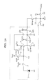
- FIG. 3 illustrates a structure of a basic circuit of the solid-state imaging device according to the first embodiment of the present invention.
- the solid-state imaging device includes a photodiode 1 , Metal Oxide Semiconductor (MOS) transistors 2 , 3 , 4 , 7 , 8 , 9 , and 12 , a storing unit 5 , a voltage setting unit 6 , capacitors 10 and 11 , and an accumulating unit 13 .
- MOS Metal Oxide Semiconductor
- the photodiode 1 is a light-receiving element that generates an optical signal charge according to an intensity of light entering the light-receiving element.
- the MOS transistor 2 is included in a transferring unit, and is a transfer gate for transferring the signal charge generated in the photodiode 1 to the accumulating unit 13 .
- the MOS transistor 2 conducts electricity, the charge generated in the photodiode 1 is transferred to the accumulating unit 13 . Then, a voltage corresponding to the charge is generated in the accumulating unit 13 .
- the MOS transistor 3 is a reset transistor that resets a voltage in the accumulating unit 13 to be an initial voltage V RST , and is included in a reset unit.
- the MOS transistor 4 is included in a circuit unit, and functions as a source follower in combination with the MOS transistor 7 .
- the storing unit 5 stores a voltage corresponding to a voltage in the accumulating unit 13 .
- the voltage setting unit 6 is a voltage setting circuit that sets a voltage in the accumulating unit 13 to a voltage corresponding to a signal stored in the storing unit 5 .
- the MOS transistor 8 functions as a switch for selecting a pixel row.
- a pixel includes a portion enclosed by a dashed line in FIG. 3 .
- the MOS transistors 9 and 12 , and the capacitors 10 and 11 form a noise canceller. A difference between an output voltage in a state where a pixel is reset and an output voltage corresponding to an optical signal charge is outputted from the noise canceller, thus reducing offset voltage variations in respective pixels.
- the reset unit may be combined with the voltage setting unit 6 .
- the reset circuit may use a part of the voltage setting unit 6 .
- the accumulating unit 13 is included in a charge combining unit, and combines a signal voltage generated through transferring of an optical signal charge generated from a light-receiving element by the transferring unit, and a voltage set by the voltage setting unit.
- FIG. 4 illustrates a circuit diagram embodying the structure of the basic circuit of the solid-state imaging device illustrated in FIG. 3 .
- the storing unit and the voltage setting unit in FIG. 3 are illustrated with specific circuit elements in FIG. 4 .
- the solid-state imaging device in FIG. 4 includes the photodiode 1 , the MOS transistors 2 , 3 , 4 , 7 , 9 , and 12 , MOS transistors 21 , 23 , and 24 , the capacitors 10 and 11 , a capacitor 22 , and the accumulating unit 13 .
- the storing unit 5 and the voltage setting unit 6 in FIG. 4 are illustrated in specific circuit elements.
- FIG. 4 differs from FIG. 3 in excluding the MOS transistor 8 therein.
- FIG. 4 although the MOS transistor 7 is not included in the pixel enclosed by the dashed line, it is provided in every column signal line connected to pixel units arranged in an identical column.
- the circuit elements in FIG. 4 that are different from those of FIG. 3 are hereinafter described in details except for the common elements described for FIG. 3 .
- the MOS transistor 8 described in FIG. 3 is a switch for selecting a pixel row. For example, after charge combining units for all pixels in a circuit as illustrated in FIG. 4 are grounded using the reset circuits and other units, each of the MOS transistors 8 may select a row, read the selected row by setting, in the charge combining unit, a value corresponding to a voltage in a corresponding storing unit, and read the next row by grounding the charge combining unit. Furthermore, non-selected rows may be certainly turned off by controlling, as a signal, V DDCEL connected to the MOS transistor 4 for each row.
- MOS transistor 7 is provided not for each pixel but for each column signal line in order to reduce the number of circuit elements, the MOS transistor 7 may be provided for each pixel.
- a combination of the MOS transistor 21 and the capacitor 22 functions as a storing unit that stores a voltage corresponding to a voltage in the accumulating unit 13 .
- a terminal of the capacitor 22 is grounded.
- a combination of the MOS transistors 23 and 24 functions as a voltage setting unit that sets a voltage in the accumulating unit 13 to a voltage corresponding to a charge amount in the capacitor 22 .
- the MOS transistor 23 has a gate terminal connected to the capacitor 22 , a drain terminal connected to the power supply voltage V DD , and a source terminal connected to a drain terminal of the MOS transistor 24 .
- the MOS transistor 23 supplies a voltage corresponding to the gate voltage to the drain terminal.
- the MOS transistor 24 has the gate terminal connected to a control signal line RD, and the source terminal connected to the accumulating unit 13 .
- the MOS transistor 24 sets a voltage in the accumulating unit 13 to a voltage in the drain terminal of the MOS transistor 24 .
- an optical signal charge received in the photodiode 1 is accumulated in the accumulating unit 13 through the MOS transistor 2 .
- a voltage corresponding to the accumulated charge is stored in the capacitor 22 through the MOS transistor 21 .
- the stored voltage is set in the accumulating unit 13 through the MOS transistors 23 and 24 .
- the voltage corresponding to the optical signal charges in the accumulating unit 13 is temporarily stored in the storing unit, and is reset in the accumulating unit 13 by the voltage setting unit 6 as necessary.
- the signal voltages that are cumulatively added are not influenced by voltage level variation in the accumulating unit 13 according to the passage of time.
- terminals of TRAN, RST, WRT, and RD are respectively provided for each pixel row, and an output terminal of the MOS transistor 4 (a terminal that is not connected to V DDCEL ) is commonly connected to a column signal line 90 for each pixel column.
- FIG. 5 illustrates a circuit structure of a solid-state imaging device of a first variation according to the first embodiment of the present invention.
- the solid-state imaging device in FIG. 5 includes the photodiode 1 , the MOS transistors 2 , 3 , 4 , 7 , 9 , 12 , 21 , 23 , and 24 , the capacitors 10 and 11 , a capacitor 32 , and the accumulating unit 13 .
- the circuit structure illustrated in FIG. 5 differs from the circuit structure in FIG. 4 in the capacitor 32 having a terminal that is not grounded. Circuit elements in FIG. 5 that are different from those of FIG. 4 are hereinafter described in details except for the common elements described for FIG. 4 .
- a terminal of the capacitor 32 is not grounded, but is connected to a control signal line CP.
- the connection compensates a voltage drop.
- a voltage in a source terminal of the MOS transistor 23 (terminal connected to the MOS transistor 24 ) drops only by a threshold voltage V T from a voltage V G that is applied to a gate terminal of the MOS transistor 23 .
- a bias voltage in the control signal line CP is applied to the capacitor 32 .
- a potential of the capacitor 32 is boosted by the voltage V T , and the MOS transistor 23 outputs a drain voltage having the same voltage value as that of a voltage held in the capacitor 32 .
- a voltage in the capacitor 32 that is a part of a storing unit is compensated for a voltage drop occurring in the MOS transistor 23 , and the resulting voltage is set in the accumulating unit 13 .
- signal voltages corresponding to respective optical signal charges are cumulatively added in the accumulating unit 13 .
- FIG. 6 illustrates a structure of a solid-state imaging device of a second variation according to the first embodiment of the present invention.
- the solid-state imaging device in FIG. 6 includes the photodiode 1 , the MOS transistors 2 , 3 , 4 , 7 , 9 , 12 , and 21 , the capacitors 10 , 11 , and 22 , the accumulating unit 13 , and a buffer circuit 41 .
- the circuit structure illustrated in FIG. 6 differs from the circuit structure in FIG. 4 in including the buffer circuit 41 instead of the MOS transistors 23 and 24 .
- Circuit elements in FIG. 6 that are different from those of FIG. 4 are hereinafter described in details except for the common elements described for FIG. 4 .
- An input terminal of the buffer circuit 41 is connected to the capacitor 22 , and an output terminal of the buffer circuit 41 is connected to the accumulating unit 13 .
- the control signal line RD controls on/off of the buffer circuit 41 .
- a circuit of series of two inverter circuits may be given as an example of a structure of the buffer circuit 41 .
- a circuit having an amplification factor 1 using an operational amplifier is used as a buffer circuit.
- Such a structure enables a voltage in the capacitor 22 that functions as a storing unit to be set in the accumulating unit 13 without any voltage drop caused by the voltage setting unit 6 .
- signal voltages corresponding to respective optical signal charges are cumulatively added with precision in the accumulating unit 13 .
- FIG. 7 illustrates a drive timing chart of the solid-state imaging device of the first variation according to the first embodiment of the present invention.
- a voltage level of control signals RST and WRT becomes high, and a voltage in a contact point between the capacitor 32 and the MOS transistor 21 that functions as a storing unit, and a voltage in the accumulating unit 13 are initialized by an initial voltage V RST . Furthermore, a voltage level of a control signal CL becomes high, and a voltage level of an output terminal OUT becomes V NCDC at the time t 1 .
- a voltage level of a control signal TRAN of the MOS transistor 2 becomes high, and an optical signal charge generated in the photodiode 1 during a period TL is transferred to the accumulating unit 13 . Furthermore, a potential of the terminal OUT is changed by an amount of a voltage in the accumulating unit 13 that is subtracted from V NCDC .
- the changed amount of voltage is obtained by allocating, to the capacitors 10 and 11 in proportion to a capacitance in the capacitor 10 and a capacitance in the capacitor 11 , a product of a voltage changed in the accumulating unit 13 and a gain in a source follower including the MOS transistors 4 and 7 .
- a potential of the terminal OUT may have the property of reflecting a change in a potential of the accumulating unit 13 .
- the voltage level of WRT becomes high, and the charges transferred to the accumulating unit 13 are allocated to accumulating unit 13 and the capacitor 32 , respectively in proportion to a capacitance in the accumulating unit 13 and a capacitance in the capacitor 32 .
- the potential of the terminal OUT varies according to the passage of time.
- a crystal defect or a dark current causes generation of a negative charge in the accumulating unit 13 , thus further reducing the potential from the time t 3 . Since an operation, as if a charge was transferred from the photodiode 1 , is performed despite no transferring from the photodiode 1 , the potential is reduced. Such reduction normally causes defects referred to as “white defects”.
- a voltage in the accumulating unit 13 needs to be set to a fixed reference voltage.
- the present invention solves such a “white defect” problem in operations after a time t 4 in the solid-state imaging device.
- the voltage of the capacitor 32 is boosted by a voltage in the control signal line CP. Then, the voltage in the accumulating unit 13 is set to a voltage corresponding to the voltage stored in the capacitor 32 through the MOS transistor 24 .
- a voltage approximately identical to that of the capacitor 32 is set in the accumulating unit 13 by boosting the voltage in the control signal line CP by V T .
- the voltage level of the control signal TRAN of the MOS transistor 2 becomes high again, and an optical signal charge generated in the photodiode 1 during the period TS is transferred to the accumulating unit 13 .
- the voltage level of WRT becomes high, and the voltage set in the accumulating unit 13 at the time t 5 is added to the voltage set in the accumulating unit 13 at the time t 4 .
- the resulting voltage obtained by adding the voltage accumulated in the accumulating unit 13 during the period TL and the voltage accumulated in the accumulating unit 13 during the period TS is allocated to the accumulating unit 13 and the capacitor 32 , respectively in proportion to a capacitance in the accumulating unit 13 and a capacitance in the capacitor 32 .
- the same processing is performed in the same manner as at the time t 4 , and the resulting voltage obtained by adding the voltage accumulated in the accumulating unit 13 during the period TL and the voltage accumulated in the accumulating unit 13 during the period TS is set in the accumulating unit 13 .
- the respective signals generated during the periods, TL, TS, and TVS are added in the accumulating unit 13 with precision, and an amount of a voltage corresponding to addition of respective signals obtained during the times t 2 , t 5 , t 8 is outputted to the terminal OUT.
- the solid-state imaging device makes it possible to store voltages each corresponding to an optical signal charge generated in a light-receiving element, to set the resulting voltage in the accumulating unit 13 using the voltage setting unit 6 , and to transfer, to the accumulating unit 13 , an optical signal charge newly generated in a light-receiving element.
- a combination of optical signal charges in a pixel is completed with precision.
- capacitance elements in a storing unit such as a MOS capacitor and a Metal Insulation Metal (MIM) capacitor, are used to achieve a function of storing a voltage signal with less noise caused by current leakage and other factors.
- MIM Metal Insulation Metal
- FIG. 8 illustrates a drive timing chart of a solid-state imaging device of a third variation according to the first embodiment of the present invention.
- the circuit structure is the same as that of FIG. 5 .
- a driving method used in FIG. 8 includes detecting signals in ascending order of light exposure times in length.
- FIG. 8 differs from FIG. 7 in illustrating timing when one row is selected from among pixel rows and a corresponding signal is read.
- optical signals are stored, transferred, and combined in all pixels simultaneously.
- the signals are read from each of the pixels by scanning each pixel row, thus enabling a global shutter operation.
- various control signals are controlled by a driving unit that is not included in the solid-state imaging device.
- a driving unit including such a driving unit is described.
- FIG. 9 illustrates a functional structure of a solid-state imaging apparatus including the solid-state imaging device according to the present invention.
- the solid-state imaging device in FIG. 9 includes a pixel unit 141 , noise cancellers 142 , a vertical shift register 143 , a horizontal shift register 144 , a driving unit 145 , a pixel power supply unit 146 , and an amplifier 147 .
- the pixel unit 141 includes light-receiving elements, transferring units, accumulating units, storing units, voltage setting units, and a portion of circuit units, and has functions of combining charge signals respectively received in different exposure times to generate the signal voltage.
- Each of the noise cancellers 142 includes a portion of the circuit units, and a function of reading voltages accumulated in a corresponding accumulating unit with precision.
- the vertical shift register 143 reads a pixel row selected in response to an instruction from the driving unit 145 .
- the horizontal shift register 144 reads a pixel column selected in response to an instruction from the driving unit 145 .
- the driving unit 145 controls the pixel unit 141 , the noise cancellers 142 , the vertical shift register 143 , and the horizontal shift register 144 .
- the pixel power supply unit 146 supplies a constant electric current to the pixel unit 141 .
- the amplifier 147 amplifies a signal voltage obtained in the pixel unit 141 .
- the driving unit 145 sets a voltage level of the control signals RST, TRAN, and WRT to be high simultaneously in all of the pixels.
- the photodiode 1 , the accumulating unit 13 , and a contact point between the MOS transistor 21 and the capacitor 32 are initialized by an initial voltage V RST .
- the driving unit 145 sets a voltage level of the control signal RST to be high again, and resets a voltage of the accumulating unit 13 , where the voltage varies easily, to the initial voltage V RST .
- the driving unit 145 sets a voltage level of TRAN to be high, and a charge generated in the photodiode 1 is transferred to the accumulating unit 13 . Then, the voltage level of WRT becomes high, and a capacitance in the accumulating unit 13 and a capacitance in the capacitor 32 are coupled. A part of the charge is moved to the capacitor 32 according to an amount of the capacitance allocated to the capacitor 32 from the coupled capacitance.
- V FD ′ C S /(C S +C FD ) ⁇ V FD
- a capacitance in the accumulating unit 13 is C FD
- a capacitance in the capacitor 32 is C S
- a voltage in the accumulating unit 13 before coupling the capacitance is V FD
- the voltage after the coupling is V FD ′.
- the driving unit 145 sets a voltage level of the control signal RD to be high, and sets, in the accumulating unit 13 , a voltage corresponding to the signal charge accumulated during the period E 1 . Then, when the driving unit 145 sets TRAN to be high, the optical signal charges accumulated during the period E 2 are transferred to the accumulating unit 13 , and signals corresponding to the charges are combined.
- the driving unit 145 sets a voltage level of WRT to be high, and the combined signals are stored in the respective storing units in the pixel unit 141 .
- the operations up to this stage namely, global shutter operations are simultaneously performed in all of the pixels in a chip.
- the driving unit 145 initializes the initial voltage V RST to be 0 V in all of the pixels and sets a voltage level of RST to be high, the voltage in the accumulating unit 13 becomes 0 V, and the MOS transistor 4 is turned off. As a result, no signal is outputted to the column signal line 90 .
- the driving unit 145 operates the vertical shift register 143 per column.
- a voltage level of RST only in rows selected by the vertical shift register 143 becomes low, and the voltage level of RD becomes high.
- a voltage corresponding to the combined signals is set in the accumulating unit 13 .
- the MOS transistor 4 that functions as a source follower in combination with the MOS transistor 7 through the column signal line 90 is turned on, and a voltage corresponding to the voltage in the accumulating unit 13 is outputted to the column signal line 90 .
- the driving unit 145 When noise is removed using Correlated Double Sampling (CDS), first, the driving unit 145 resets a voltage in the MOS transistor 3 to a reset voltage V RST at the time t 15 b and sets a voltage level of RST to be high. Thus, an initial state indicating no light input is set in the accumulating unit 13 , and the state is stored in the storing unit. Next, a voltage corresponding to the initial state stored at the time t 15 c is set in the accumulating unit 13 , thus obtaining an output signal when the MOS transistor 3 is reset. By detecting a difference between the reset output voltage and the combined signal output voltage, functional variations in the pixels of the MOS transistor 4 may be reduced.
- CDS Correlated Double Sampling
- an image is exposed to high-intensity light for a short period of time, and then, another light is exposed to the image for a long period of time.
- noise may be reduced by light having low and medium luminance, and much higher definition images may be obtained.
- the circuit structure illustrated in FIG. 10 differs from the circuit structure in FIG. 5 in excluding the MOS transistor 4 . Furthermore, the MOS transistor 8 that is illustrated in FIG. 3 and that selects a pixel is inserted between the MOS transistor 23 and the column signal line 90 . Since the circuit structure in FIG. 10 is the same as that of FIG. 5 in an operation for accumulating an optical signal charge for a plurality of times, the description is omitted.
- the fourth variation of the first embodiment is characterized in an operation for reading signal charges accumulated, and thus the feature is hereinafter described in details.
- FIG. 11 illustrates a drive timing chart of the solid-state imaging device of the fourth variation according to the first embodiment of the present invention.
- Optical signals are stored, transferred, and combined in all pixels simultaneously, and when signals are read from each of the pixels by scanning each row, a global shutter operation can be performed.
- the global shutter operation is the same as operations in the third variation illustrated in FIG. 8 , that is, operations from the time t 10 to the time t 14 , and operations to be performed when a voltage level of WRT becomes high after the time t 14 and the combined signals are stored in the capacitor 32 .
- a low voltage is applied to a control terminal SN of the MOS transistor 8 , and the pixel and the column signal line 90 are separated from each other.
- an operation for reading a signal obtained by combining 3 different signals respectively generated during the periods E 1 , E 2 , and E 3 is described.
- the driving unit 145 initializes the initial voltage V RST to be 0V in all of the pixels and sets the voltage level of RST to be high, the voltage in the accumulating unit 13 becomes 0V, and the MOS transistor 4 is turned off. As a result, no signal is outputted to the column signal line 90 .
- the driving unit 145 operates the vertical shift register 143 per column, and sets the voltage level of the control terminal SN in a row selected by the vertical shift register 143 to be high. Thereby, the MOS transistor 8 is turned on. Through these operations, the pixel is connected to the column signal line 90 , and the MOS transistors 7 and 23 are connected in series, thus forming a source follower circuit and outputting, to the column signal line 90 , a signal corresponding to the voltage stored in the capacitor 32 .
- an initial state where no light is inputted is stored in the capacitor 32 by setting the voltage level of RST and WRT to be high using the driving unit 14 at the time t 15 b .
- a reset signal corresponding to a gate voltage corresponding to the initial state stored is outputted from the MOS transistor 23 .
- the voltage setting unit serves as a part of a source follower circuit that outputs a signal, and has an advantage of reducing the number of circuit elements included in a pixel.
- FIG. 12 illustrates a structure of the solid-state imaging device of a fifth variation according to the first embodiment of the present invention.
- the solid-state imaging device in FIG. 12 includes the photodiode 1 , the MOS transistors 2 , 7 , 8 , 9 , 12 , 21 , 23 , and 24 , the capacitors 10 , 11 , and 32 , and the accumulating unit 13 .
- the circuit structure illustrated in FIG. 12 differs from the circuit structure in FIG. 10 in excluding the MOS transistor 3 . Furthermore, although a source terminal of the MOS transistor 7 is grounded in FIG. 10 , a control signal IN is applied to the source terminal of the MOS transistor 7 in the fifth variation. Since the circuit structure in FIG. 12 is the same as those of FIGS. 4 , 5 , and 10 in the operation for accumulating an optical signal charge for a plurality of times, the description is omitted.
- the fifth variation of the first embodiment is characterized in a reset operation, thus the feature is described in details.
- FIG. 13 illustrates a drive timing chart of the solid-state imaging device of the fifth variation according to the first embodiment of the present invention.
- Optical signals are stored, transferred, and combined in all pixels simultaneously, and when signals are read from each of the pixels by scanning each row, a global shutter operation can be performed.
- FIG. 13 differs from an operation for resetting the initial voltage V RST in the third variation illustrated in FIG. 8 .
- the reset operation is performed at the times t 10 , t 11 , and t 15 .
- a control terminal LG of the MOS transistor 7 is turned on by applying a power supply voltage V DD thereto, and the initial voltage V RST is applied to IN.
- the voltage level of the terminals SN, RD, and WRT is set to be high to reset the voltage in the accumulating unit 13 and the capacitor 32 .
- the voltage level of the terminals SN and RD is set to be high to reset the voltage in the accumulating unit 13 .
- a voltage V LG is applied to a control terminal LG of the MOS transistor 7 , and IN indicates a grounding potential.
- the voltage V LG is selected to keep a linear relationship between the voltage stored in the capacitor 32 and the signal voltage outputted to the column signal line 90 , and to prevent saturation of the output voltage.
- the MOS transistor 7 included in the source follower circuit also functions as a reset circuit, thus bringing an advantage of reducing the number of circuit elements included in a pixel. Furthermore, the structure can omit a wiring where the reset voltage V RST and a control signal RST in an reset operation are applied to a pixel, thus reducing an area for each solid-state imaging device.
- FIG. 14A illustrates a structure of a solid-state imaging device of a sixth variation according to the first embodiment of the present invention.
- the solid-state imaging device in FIG. 14A includes the photodiode 1 , the MOS transistors 2 , 4 , 7 , 8 , 9 , and 12 , MOS transistors 81 , 82 , 83 , 85 , 86 , and 88 , the capacitors 10 and 11 , a capacitor 87 , the accumulating unit 13 , and a source follower output point 47 , and a buffer circuit 84 .
- FIG. 14A differs from FIG. 3 in the structure where functions of a storing unit, a reset unit, and a voltage setting unit are shared among circuit elements, and where the reset unit is not independently provided in each circuit. Circuit elements in FIG. 14A that are different from those of FIG. 3 are hereinafter described in details except for the common elements described for FIG. 3 .
- the buffer circuit 84 may be the buffer circuit 80 including an inverting circuit having two inverter circuits as illustrated in FIG. 14B .
- a pixel includes a portion enclosed by a dashed line in FIG. 14A .
- FIG. 15 illustrates a drive timing chart of the solid-state imaging device of the sixth variation according to the first embodiment of the present invention. Furthermore, V FD in FIG. 15 indicates a potential of the accumulating unit 13 . Furthermore, the MOS transistor 8 is a switch for selecting a pixel row. During a time period when signal voltages are combined in a pixel and in a noise canceller, the MOS transistor 8 is turned on all the time.
- the voltage level of gate terminals C 81 , C 82 , C 86 , C 88 , CL, and SH becomes high, and thus the MOS transistors 81 , 82 , 86 , 88 , 12 , and 9 are turned on.
- a bias voltage in the terminal C 89 is applied to the accumulating unit 13 , and the voltage V NCDC is applies to the terminal OUT that is a contact point between the capacitors 10 and 11 .
- the voltage level of TRAN becomes high, and an optical signal charge generated in the photodiode 1 during the period TL is transferred to the accumulating unit 13 through the MOS transistor 2 .
- a potential of the accumulating unit 13 is lower than that of C 89 .
- the voltage level of the gate terminals C 81 , C 82 , and C 85 becomes high, and thus the MOS transistors 81 , 82 , and 85 are turned on.
- a voltage value of the accumulating unit 13 is stored in the capacitor 87 through the buffer circuit 84 .
- a crystal defect or a dark current causes generation of a negative charge in the accumulating unit 13 as described above, thus further reducing the potential from the time t 93 according to the passage of time.
- the voltage level of the gate terminals C 81 , C 83 , and C 86 becomes high, and thus the MOS transistors 81 , 83 , and 86 are turned on.
- a voltage value of the capacitor 87 is set in the accumulating unit 13 through the buffer circuit 84 .
- the accumulating unit 13 is not influenced by voltage variations caused by white defects due to setting of a voltage at the time t 93 .
- Operations from the time t 95 to t 97 are performed in the same manner as from the time t 92 to t 94 , and the voltage level of TRAN becomes high at the time t 98 to turn on the MOS transistor 2 .
- These operations correspond to transferring of an optical signal charge generated in the photodiode 1 during the periods TL, TS, and TVS sequentially. In other words, respective signals generated during the periods TL, TS, and TVS are combined in the accumulating unit 13 .
- a changed amount of the voltage in the accumulating unit 13 is transmitted to the terminal OUT through the MOS transistors 4 and 7 that function as a source follower.
- the changed amount may be determined by an equation, ⁇ a changed amount of voltage in the accumulating unit 13 ⁇ a gain in the source follower ⁇ (a proportion of a capacitance in the capacitor 10 and a capacitance in the capacitor 11 ) ⁇ .
- a difference between a voltage in the terminal OUT and V NCDC at the time t 99 is set as a value of combined voltage signals generated during the periods TL, TS, and TVS.
- FIG. 14A illustrating the circuit structure of the solid-state imaging device of the sixth variation according to the first embodiment to the structure of the basic circuit in FIG. 3
- the MOS transistors 81 , 82 , 86 , and 88 correspond to the reset unit in FIG. 3
- the MOS transistors 81 , 82 , and 85 correspond to the storing unit in FIG. 3
- the MOS transistors 81 , 83 , and 86 , and the buffer circuit 84 correspond to the voltage setting unit in FIG. 3 .
- FIG. 16 illustrates a structure of a solid-state imaging device of a seventh variation according to the first embodiment of the present invention.
- the solid-state imaging device in FIG. 16 includes the photodiode 1 , the MOS transistors 2 , 3 , 4 , 7 , 8 , 9 , and 12 , MOS transistors 102 and 103 , the capacitors 10 and 11 , capacitors 104 and 105 , the accumulating unit 13 , a pixel output point 34 , and the source follower output point 47 .
- FIG. 16 has a circuit structure including a reset unit that is provided independently as in FIG. 3 , but differs from FIG. 3 in that each circuit element shares functions of a storing unit and a voltage setting unit. Circuit elements in FIG. 16 that are different from those of FIG. 3 are hereinafter described in details except for the common elements described for FIG. 3 .
- Capacitors 104 and 105 are connected at a pixel output point 34 .
- a pixel includes a portion enclosed by a dashed line in FIG. 16 .
- FIG. 17 illustrates a timing chart of the solid-state imaging device of the seventh variation according to the first embodiment of the present invention. Furthermore, V FD in FIG. 17 indicates a potential of the accumulating unit 13 . Furthermore, the MOS transistor 8 is a switch for selecting a pixel row. During a time period when signal voltages are combined in the pixel and in the noise canceller, the MOS transistor 8 is turned on all the time.
- the voltage level of RST, C 102 , C 103 , SH, and CL becomes high, and the MOS transistors 3 , 9 , 12 , 102 , and 103 are turned on.
- V 4 When a difference between a gate terminal of the MOS transistor 4 and the source follower output point 47 is defined as a voltage difference V 4 , the voltage V RST is applied to a contact point between a capacitor 104 and the MOS transistor 102 , a voltage value (V RST ⁇ V 4 ) is applied to the pixel output point 34 , and the V 4 is stored in the capacitor 104 . The voltage value (V RST ⁇ V 4 ) is also applied to the capacitor 105 .
- the voltage level of TRAN becomes high, and the optical signal charge generated in the photodiode 1 during the period TL is transferred to the accumulating unit 13 through the MOS transistor 2 . Since the generated charge has a negative characteristic, a potential of the accumulating unit 13 is lower than that of V RST .
- V TL the voltage in the accumulating unit 13 is defined as a voltage value (V RST ⁇ V TL ).
- a voltage value (V RST ⁇ V TL ⁇ V 4 ) is stored in the capacitor 105 through the MOS transistor 103 . Since the capacitor 104 stores the voltage value V 4 , a voltage value of the contact point between the capacitor 104 and the MOS transistor 102 is defined as ⁇ (V RST ⁇ V TL ⁇ V 4 )+V 4 ⁇ that is the same as the voltage value (V RST ⁇ V TL ) in the accumulating unit 13 .
- the voltage level of C 102 becomes high, and the MOS transistor 102 conducts electricity.
- the voltage stored in the capacitor 104 is transmitted to the accumulating unit 13 , and the voltage in the accumulating unit 13 is set to a voltage value (V RST ⁇ V TL ) at the time t 113 .
- the operations from the time t 115 to t 117 are performed in the same manner as from the time t 112 to t 114 , and the voltage level of TRAN becomes high at the time t 118 to turn on the MOS transistor 2 .
- These operations correspond to transferring of an optical signal charge generated in the photodiode 1 during the periods TL, TS, and TVS sequentially to the accumulating unit 13 .
- respective signals generated during the periods TL, TS, and TVS are combined in the accumulating unit 13 .
- a changed amount of the voltage in the accumulating unit 13 is transmitted to the terminal OUT through the MOS transistors 4 and 7 that function as a source follower.
- the changed amount may be determined by ⁇ a changed amount of voltage in the accumulating unit 13 ⁇ a gain of source follower ⁇ (a proportion of a capacitance in the capacitor 10 and a capacitance in the capacitor 11 ) ⁇ .
- a difference between a voltage in the terminal OUT and V NCDC at the time t 119 is set as a value of combined voltage signals during the periods TL, TS, and TVS.
- FIG. 16 Comparing FIG. 16 illustrating the circuit structure of the solid-state imaging device of the seventh variation according to the first embodiment to the structure of the basic circuit in FIG. 3 , the MOS transistor 3 corresponds to the reset unit in FIG. 3 , the MOS transistors 103 , 104 , and 105 correspond to the storing unit in FIG. 3 , and the MOS transistor 102 corresponds to the voltage setting unit in FIG. 3 .
- the solid-state imaging device includes in a pixel: a charge combining unit that combines signal voltages each corresponding to optical signal charges of light generated in light-receiving elements; a storing unit that stores the voltage combined by the charge combining unit; and a voltage setting unit that sets, in the charge combining unit, a value corresponding to the voltage in the storing unit.
- voltages corresponding to respective optical signal charges generated in a plurality of exposure times are added in a pixel for a short period of time without any influence of voltage variations according to the passage of time in the charge combining unit.
- a dynamic range may be expanded without any external circuit.
- the driving method of the solid-state imaging device described in the third variation of the first embodiment is not only achieved by a solid-state imaging apparatus including the solid-state imaging device illustrated in FIG. 5 but also by the basic circuit illustrated in FIG. 3 and by a solid-state imaging apparatus including the solid-state imaging device illustrated in FIGS. 4 , 6 , 14 , and 16 .
- FIG. 18A illustrates a functional block diagram of a solid-state imaging apparatus including the solid-state imaging device according to the first embodiment of the present invention
- FIG. 18B illustrates a functional block diagram of a conventional solid-state imaging apparatus.
- the solid-state imaging apparatus illustrated in FIG. 18A combines, in pixel units of a solid-state imaging device 71 , signals generated during a period TL and a period TS, and further a signal generated during a period TVS.
- an output signal generated in the pixel units of the solid-state imaging device 71 is regarded as a combined image.
- the conventional solid-state imaging apparatus illustrated in FIG. 18B stores signals, sig 1 , sig 2 , and sig 3 generated in a solid-state imaging device 72 respectively during periods TL, TS, and TVS, in a circuit 73 outside the solid-state imaging device. Then, a combining unit in the circuit 73 combines the signals to generate a combined image.
- the solid-state imaging device does not need a storing unit and an image combining unit outside the solid-state imaging device, even when a specification and design of a dynamic range need to be changed, the solid-state imaging device has such an advantage that a pixel unit in a solid-state imaging device has only to be changed without any considerable influence on an external system.
- MOS sensors perform a rolling shutter operation where light is sequentially exposed to rows, and respective signals are outputted from the sensors.
- an image to be taken is distorted.
- the first embodiment achieves a global shutter operation that a screen image is exposed to light at once, the screen image is never distorted.
- the solid-state imaging device that achieves such a global shutter operation is significantly advantageous for a vehicle-mounted camera and a machine vision that are used for shooting a subject by a person who is moving or for shooting a moving subject.
- the present invention is very advantageous not only for expanding a dynamic range by combining signal charges (in other words, multiple exposure) that have been accumulated during a plurality of exposure times, but also for enabling a global shutter operation even when a charge accumulated during a single exposure time is outputted, for example.
- the present invention also covers capturing of an image through one-time light exposure.
- a solid-state imaging device includes in a pixel: an accumulating unit that accumulates an optical signal charge generated in a light-receiving element; a reset unit that resets a voltage in the accumulating unit; a difference circuit unit that adds a difference voltage between a signal voltage in the accumulating unit and a voltage reset in the reset unit; a storing unit that stores a signal voltage in the difference circuit unit; and a voltage setting unit that sets, in the difference circuit unit, a voltage in the storing unit.
- voltages corresponding to respective optical signal charges generated in a plurality of exposure times can be added in a pixel for a short period of time.
- FIG. 19 illustrates a structure of a circuit of the solid-state imaging device according to the second embodiment of the present invention.
- the solid-state imaging device in FIG. 19 includes a photodiode 1 , MOS transistors 2 , 3 , 4 , 7 , 8 , 9 , 121 , 122 , 124 , and 125 , capacitors 10 , 11 , and 126 , a source follower output point 47 , an accumulating unit 120 , and a buffer circuit 123 .
- FIG. 19 differs from FIG.
- the MOS transistors 121 , 122 , 124 , and 125 that are circuit elements that functions as a storing unit and a voltage setting unit, the capacitor 126 , and the buffer circuit 123 are provided for each column signal line.
- the photodiode 1 is a light-receiving element that generates an optical signal charge according to an intensity of light entering the light-receiving element.
- the MOS transistor 2 is included in a transferring unit, and has a function of transferring an optical signal charge generated in the photodiode 1 to the accumulating unit 120 .
- the MOS transistor 3 is included in the reset unit, and has a function of resetting a voltage in the accumulating unit 120 .
- the MOS transistors 9 and 12 , and the capacitors 10 and 11 are included in the difference circuit unit, and have a function of combining a difference voltage between a signal voltage and a reset voltage in the accumulating unit 120 , and a reference voltage set by the voltage setting unit.
- an initial value of the reference voltage is V NCDC .
- the MOS transistors 121 and 124 , the buffer circuit 123 , and the capacitor 126 are included in the storing unit, and have a function of storing a voltage obtained by combining voltages in the difference circuit unit.
- the MOS transistors 122 and 125 , and the buffer circuit 123 are included in the voltage setting unit, and have a function of setting a voltage held in the storing unit as a reference voltage in the difference circuit.
- the MOS transistors 4 and 7 are included in a circuit unit, and have a function of reading a voltage in the accumulating unit 120 .
- each of the accumulating unit 120 , the reset unit, and the difference circuit unit has a distinctive function, and they compose one charge combining unit that has a function of combining voltages corresponding to optical signal charges.
- a gain in the buffer circuit 123 is 1.
- the buffer circuit 123 is made up of, for example, a buffer circuit 80 including an inverting circuit having two inverter circuits illustrated in FIG. 14B or an operational amplifier.
- a pixel includes a portion enclosed by a dashed line in FIG. 19 .
- the driving operations of each circuit element are hereinafter exemplified to describe a function of the circuit structure.
- FIG. 20 illustrates a timing chart of the solid-state imaging device of the second embodiment of the present invention. Furthermore, V FD in FIG. 20 indicates a potential of the accumulating unit 120 . Furthermore, the MOS transistor 8 is a switch for selecting a pixel row.
- the voltage level of RST, C 121 , C 124 , SH, and CL becomes high, and the MOS transistors 3 , 121 , 124 , 9 , and 12 are turned on.
- the voltage V RST is applies to the accumulating unit 120
- the voltage V NCDC is applies to a terminal OUT.
- V NCDC is stored in a capacitor 126 through the MOS transistors 121 and 124 , and the buffer circuit 123 .
- the voltage level of TRAN becomes high, and the signal charge generated in the photodiode 1 during the period TL is transferred to the accumulating unit 120 through the MOS transistor 2 . Since the generated charge has a negative characteristic, a potential of the accumulating unit 120 is lower than that of V RST .
- V TL the voltage of the accumulating unit 120 is defined as a voltage (V RST ⁇ V TL ).
- an amount of the voltage varied from V NCDC is defined as ⁇ k ⁇ ( ⁇ V TL ) ⁇ that is an amount of a voltage corresponding to an output signal of light received by the photodiode 1 during the period TL.
- k is determined using an equation, ⁇ a gain in a source follower ⁇ (a proportion of a capacitance in the capacitor 10 and a capacitance in the capacitor 11 ) ⁇ .
- the capacitor 126 stores a voltage value [V NCDC ⁇ k ⁇ (V RST ⁇ V TL ) ⁇ ]
- the voltage level of RST, C 122 , C 125 , and SH becomes high, and the MOS transistors 3 , 122 , 125 , and 9 are turned on.
- the voltage in the accumulating unit 120 is set again to V RST that is a reset voltage.
- the voltage in the terminal OUT is set to a voltage value [V NCDC ⁇ k ⁇ (V RST ⁇ V TL ) ⁇ ] that is held in the capacitor 126 .
- the voltage in the terminal OUT is set to V NCDC at the time t 131 , it is set to a voltage value including a voltage corresponding to the signal outputted during the period TL.
- signals outputted during respective time periods are added by setting of different voltage values for each of the time periods.
- the operations from the time t 135 to t 137 are performed in the same manner as from the time t 132 to t 134 , and the voltage level of TRAN becomes high at the time t 138 to turn on the MOS transistor 2 . Then, an optical signal charge generated in the photodiode 1 during the period TVS is transferred to the accumulating unit 120 .
- a difference circuit unit mainly serving as a charge combining unit that combines signal voltage generated during the periods TL, TS, and TVS, is not provided for each pixel.
- the difference circuit unit, the storing unit, and the voltage setting unit are provided for each column signal line, not for each pixel, the number of circuit elements and an area for the solid-state imaging device can be reduced.
- the periods TL, TS, and TVS are set to 30 msec, 300 ⁇ sec, and 3 ⁇ sec, respectively.
- reading one row by a column signal line takes 60 ⁇ sec that is defined as a time H.
- the exposure operation during the period TL may be performed simultaneously when voltages are outputted in other pixel rows.
- the exposure operation during the period TL does not influence the time H.
- the shortest exposure time of 3 ⁇ sec that is negligible to the time H does neither influence the time H.
- a signal voltage generated during the period TL is read by the difference circuit unit.
- processing capacity of the difference circuit unit is occupied by the processing of the pixel unit.
- a row to be read is changed in 60 ⁇ sec.
- the capacitor 126 is made up of five sub-capacitors that are connected in parallel, not a single sub-capacitor, and a switch can switch between the respective sub-capacitors.
- the solid-state imaging device includes in a pixel: an accumulating unit that accumulates an optical signal charge generated by a light-receiving element; a reset unit that resets a voltage in the accumulating unit; a difference circuit unit that adds a difference voltage between a signal voltage in the accumulating unit and a voltage reset in the reset unit; a storing unit that stores a signal voltage in the difference circuit unit; and a voltage setting unit that sets, in the difference circuit unit, the signal voltage in the storing unit.
- voltages corresponding to respective optical signal charges generated in a plurality of exposure times can be added in a pixel for a short period of time.
- the solid-state imaging device of the second embodiment in the present invention may also be compared with a conventional solid-state imaging device, as illustrated in FIG. 18 for the first embodiment. Since the solid-state imaging device according to the second embodiment does not need a storing unit and an image combining unit outside the solid-state imaging device, even when a specification and design of a dynamic range need to be changed, the solid-state imaging device has such an advantage that a pixel unit in a solid-state imaging device has only to be changed without any considerable influence on an external system.
- Functions of the solid-state imaging device according to the second embodiment can be exercised by connecting the MOS transistors 21 , 23 , and 24 each including a storing unit and a voltage setting unit, and the capacitor 32 including a bias voltage terminal to the terminal OUT in the circuit structure of the solid-state imaging device of the first variation according to the first embodiment of the present invention that is illustrated in FIG. 5 .
- the number of circuit elements to be needed may be reduced by arranging a simple circuit having a bias function for each column signal line, not for each pixel.
- the present invention includes a camera including a solid-state imaging apparatus 152 according to the present invention.
- This camera includes a lens 151 , a solid-state imaging apparatus 152 , a driving circuit 153 , a signal processing unit 154 , and an external interface unit 155 as illustrated in FIG. 21 .
- Light passes through the lens 151 and enters the solid-state imaging apparatus 152 .
- the signal processing unit 154 drives the solid-state imaging apparatus 152 through the driving circuit 153 to obtain an output signal from the solid-state imaging apparatus 152 .
- the signal processing unit 154 performs various signal processing on the output signal, and outputs the signal outside through the external interface unit 155 .
- the driving circuit 153 is characterized in driving the solid-state imaging apparatus 152 so that pixel units included in the solid-state imaging apparatus 152 and a signal outputted from a noise canceller have a wider dynamic range without any external circuit by setting different exposure times therein. Even when strong light or very weak light enters, such camera has an advantage of capturing a clear image, and is exemplified, for example, by a digital still camera illustrated in FIG. 22A and a video camera illustrated in FIG. 22B .
- the present invention is in particular applicable to a digital still camera and a video camera that include a solid-state imaging device, and optimally to a solid-state imaging apparatus requiring a wider dynamic range.
Landscapes
- Engineering & Computer Science (AREA)
- Multimedia (AREA)
- Signal Processing (AREA)
- Solid State Image Pick-Up Elements (AREA)
- Transforming Light Signals Into Electric Signals (AREA)
Abstract
Description
Claims (15)
Applications Claiming Priority (2)
| Application Number | Priority Date | Filing Date | Title |
|---|---|---|---|
| JP2007-226663 | 2007-08-31 | ||
| JP2007226663 | 2007-08-31 |
Publications (2)
| Publication Number | Publication Date |
|---|---|
| US20090059047A1 US20090059047A1 (en) | 2009-03-05 |
| US7956916B2 true US7956916B2 (en) | 2011-06-07 |
Family
ID=40406814
Family Applications (1)
| Application Number | Title | Priority Date | Filing Date |
|---|---|---|---|
| US12/195,584 Active 2029-09-19 US7956916B2 (en) | 2007-08-31 | 2008-08-21 | Solid-state imaging device |
Country Status (2)
| Country | Link |
|---|---|
| US (1) | US7956916B2 (en) |
| JP (1) | JP5205155B2 (en) |
Cited By (3)
| Publication number | Priority date | Publication date | Assignee | Title |
|---|---|---|---|---|
| US20100208096A1 (en) * | 2004-08-06 | 2010-08-19 | Nobuhiro Takeda | Image capturing apparatus |
| US20100289933A1 (en) * | 2008-03-14 | 2010-11-18 | Canon Kabushiki Kaisha | Image sensing device and imaging system |
| US8817143B2 (en) | 2009-04-16 | 2014-08-26 | Panasonic Corporation | Solid-state imaging device comprising a holding circuit and driving method thereof |
Families Citing this family (12)
| Publication number | Priority date | Publication date | Assignee | Title |
|---|---|---|---|---|
| JP4929075B2 (en) * | 2007-06-28 | 2012-05-09 | パナソニック株式会社 | Solid-state imaging device, driving method thereof, and imaging device |
| US7569803B2 (en) * | 2007-10-04 | 2009-08-04 | Aptina Imaging Corporation | Biasing apparatus, systems, and methods |
| JP2009267836A (en) * | 2008-04-25 | 2009-11-12 | Panasonic Corp | Solid-state imaging device, driving method thereof, and camera |
| JP5122358B2 (en) * | 2008-04-25 | 2013-01-16 | パナソニック株式会社 | Camera drive method, camera |
| JP2009303088A (en) * | 2008-06-17 | 2009-12-24 | Panasonic Corp | Solid-state imaging device, its driving method and camera |
| JP2010200025A (en) * | 2009-02-25 | 2010-09-09 | Panasonic Corp | Solid-state imaging device |
| US20150103973A1 (en) * | 2013-10-11 | 2015-04-16 | General Electric Company | X-ray system with multiple dynamic range selections |
| JP2016111378A (en) * | 2014-12-02 | 2016-06-20 | キヤノン株式会社 | Solid-state image sensor |
| CN108063905B (en) * | 2016-11-09 | 2020-04-14 | 京东方科技集团股份有限公司 | Pixel sensing circuit and driving method thereof, image sensor, electronic device |
| CN111247793B (en) | 2017-10-23 | 2022-12-16 | 索尼半导体解决方案公司 | Imaging device and electronic apparatus |
| KR102490273B1 (en) * | 2018-03-29 | 2023-01-20 | 에스케이하이닉스 주식회사 | Electronic device |
| US12328519B2 (en) * | 2022-02-15 | 2025-06-10 | Novatek Microelectronics Corp. | Image sensor |
Citations (10)
| Publication number | Priority date | Publication date | Assignee | Title |
|---|---|---|---|---|
| WO2004110057A1 (en) | 2003-06-02 | 2004-12-16 | Shoji Kawahito | Wide dynamic range image sensor |
| US20060102827A1 (en) | 2004-11-17 | 2006-05-18 | Matsushita Electric Industrial Co., Ltd. | Solid-state imaging device |
| US20060119720A1 (en) | 2004-12-03 | 2006-06-08 | Micron Technology, Inc. | Imager pixel with capacitance circuit for boosting reset voltage |
| US20060278948A1 (en) | 2005-06-08 | 2006-12-14 | Matsushita Electric Industrial Co., Ltd. | Solid-state image sensor and manufacturing method thereof |
| US20070013797A1 (en) * | 2005-07-12 | 2007-01-18 | Micron Technology, Inc. | Dual conversion gain gate and capacitor and HDR combination |
| US20070131991A1 (en) * | 2004-02-27 | 2007-06-14 | Shigetoshi Sugawa | Solid-state imaging device, line sensor and optical sensor and method of operating solid-state imaging device |
| US20070153109A1 (en) * | 2005-11-24 | 2007-07-05 | Stmicroelectronics S.A. | Image sensor element with multiple outputs |
| US20070222867A1 (en) | 2004-05-31 | 2007-09-27 | Matsushita Electric Industrial Co., Ltd. | Solid-State Imaging Device |
| US20080061216A1 (en) | 2004-07-06 | 2008-03-13 | Matsushita Electric Industrial Co., Ltd. | Solid-State Imaging Device |
| US20080129851A1 (en) | 2006-12-04 | 2008-06-05 | Matsushita Electric Industrial Co., Ltd. | Solid-state imaging device and imaging system |
Family Cites Families (9)
| Publication number | Priority date | Publication date | Assignee | Title |
|---|---|---|---|---|
| JP4081188B2 (en) * | 1998-09-16 | 2008-04-23 | オリンパス株式会社 | Image pickup apparatus using amplification type solid-state image pickup device |
| US6710804B1 (en) * | 2000-01-18 | 2004-03-23 | Eastman Kodak Company | CMOS active pixel image sensor with extended dynamic range and sensitivity |
| JP4366846B2 (en) * | 2000-08-22 | 2009-11-18 | 日本ビクター株式会社 | Solid-state imaging device |
| JP4584499B2 (en) * | 2001-06-28 | 2010-11-24 | オリンパス株式会社 | Solid-state imaging device |
| JP4135360B2 (en) * | 2001-12-25 | 2008-08-20 | ソニー株式会社 | Solid-state imaging device |
| JP4317115B2 (en) * | 2004-04-12 | 2009-08-19 | 国立大学法人東北大学 | Solid-state imaging device, optical sensor, and operation method of solid-state imaging device |
| JP2005354484A (en) * | 2004-06-11 | 2005-12-22 | Canon Inc | Amplifying memory device and solid-state imaging device |
| JP2006148328A (en) * | 2004-11-17 | 2006-06-08 | Matsushita Electric Ind Co Ltd | Solid-state imaging device |
| US8119965B2 (en) * | 2006-01-25 | 2012-02-21 | Kyocera Corporation | Image sensor having two light receiving elements and camera module having the image sensor |
-
2008
- 2008-07-15 JP JP2008183816A patent/JP5205155B2/en active Active
- 2008-08-21 US US12/195,584 patent/US7956916B2/en active Active
Patent Citations (12)
| Publication number | Priority date | Publication date | Assignee | Title |
|---|---|---|---|---|
| WO2004110057A1 (en) | 2003-06-02 | 2004-12-16 | Shoji Kawahito | Wide dynamic range image sensor |
| JP2004363666A (en) | 2003-06-02 | 2004-12-24 | Shoji Kawahito | Wide dynamic range image sensor |
| US20070103569A1 (en) | 2003-06-02 | 2007-05-10 | National University Corporation Shizuoka University | Wide dynamic range image sensor |
| US20070131991A1 (en) * | 2004-02-27 | 2007-06-14 | Shigetoshi Sugawa | Solid-state imaging device, line sensor and optical sensor and method of operating solid-state imaging device |
| US20070222867A1 (en) | 2004-05-31 | 2007-09-27 | Matsushita Electric Industrial Co., Ltd. | Solid-State Imaging Device |
| US20080061216A1 (en) | 2004-07-06 | 2008-03-13 | Matsushita Electric Industrial Co., Ltd. | Solid-State Imaging Device |
| US20060102827A1 (en) | 2004-11-17 | 2006-05-18 | Matsushita Electric Industrial Co., Ltd. | Solid-state imaging device |
| US20060119720A1 (en) | 2004-12-03 | 2006-06-08 | Micron Technology, Inc. | Imager pixel with capacitance circuit for boosting reset voltage |
| US20060278948A1 (en) | 2005-06-08 | 2006-12-14 | Matsushita Electric Industrial Co., Ltd. | Solid-state image sensor and manufacturing method thereof |
| US20070013797A1 (en) * | 2005-07-12 | 2007-01-18 | Micron Technology, Inc. | Dual conversion gain gate and capacitor and HDR combination |
| US20070153109A1 (en) * | 2005-11-24 | 2007-07-05 | Stmicroelectronics S.A. | Image sensor element with multiple outputs |
| US20080129851A1 (en) | 2006-12-04 | 2008-06-05 | Matsushita Electric Industrial Co., Ltd. | Solid-state imaging device and imaging system |
Non-Patent Citations (1)
| Title |
|---|
| English language Abstract JP 2004-363666 A. |
Cited By (5)
| Publication number | Priority date | Publication date | Assignee | Title |
|---|---|---|---|---|
| US20100208096A1 (en) * | 2004-08-06 | 2010-08-19 | Nobuhiro Takeda | Image capturing apparatus |
| US8233071B2 (en) * | 2004-08-06 | 2012-07-31 | Canon Kabushiki Kaisha | Image capturing apparatus comprising image sensor and plurality of pixels with simultaneous transfer of pixel electric charge from a first to an oppositely arranged second storage device |
| US20100289933A1 (en) * | 2008-03-14 | 2010-11-18 | Canon Kabushiki Kaisha | Image sensing device and imaging system |
| US8368785B2 (en) * | 2008-03-14 | 2013-02-05 | Canon Kabushiki Kaisha | Image sensing device and imaging system |
| US8817143B2 (en) | 2009-04-16 | 2014-08-26 | Panasonic Corporation | Solid-state imaging device comprising a holding circuit and driving method thereof |
Also Published As
| Publication number | Publication date |
|---|---|
| US20090059047A1 (en) | 2009-03-05 |
| JP5205155B2 (en) | 2013-06-05 |
| JP2009077381A (en) | 2009-04-09 |
Similar Documents
| Publication | Publication Date | Title |
|---|---|---|
| US7956916B2 (en) | Solid-state imaging device | |
| US10771718B2 (en) | Imaging device and imaging system | |
| US8089530B2 (en) | Solid-state image pickup apparatus, drive method for the solid-state image pickup apparatus, and image pickup apparatus | |
| US9473720B2 (en) | Solid-state image-capturing device and image-capturing device | |
| CN106993141B (en) | Image pickup apparatus | |
| KR101450904B1 (en) | A/d conversion circuit, control method thereof, solid-state imaging device, and imaging apparatus | |
| JP5108713B2 (en) | Solid-state imaging device and imaging device | |
| CN102970494B (en) | Imaging device, imaging method, and electronic device | |
| US7633541B2 (en) | Image pickup apparatus having a correction unit for a digital image signal | |
| US20150222830A1 (en) | Image pickup element and control method therefor, and camera | |
| US20060102827A1 (en) | Solid-state imaging device | |
| US8730365B2 (en) | Image capturing apparatus and image capturing system | |
| JP2008263546A (en) | Solid-state imaging apparatus, method for driving the solid-state imaging apparatus and imaging system using them | |
| CN102656879B (en) | Image pickup apparatus and image sensor | |
| WO2013111629A1 (en) | Solid-state image sensor, driving method therefor, and electronic device | |
| JP2024529693A (en) | A small-area self-calibrating barrier modulation pixel with multiple barriers and dual conversion gain | |
| WO2023152035A1 (en) | Image sensor, optoelectronic device including the image sensor and method for operating the image sensor | |
| JP6574653B2 (en) | Imaging apparatus and imaging system | |
| US9325924B2 (en) | Solid-state image-capturing device having lines that connect input units and electronic camera using the same | |
| US8149308B2 (en) | Solid-state image pickup device | |
| JP2009171027A (en) | Imaging device | |
| US20260039972A1 (en) | Shared high dynamic range rolling shutter architecture with lateral overflow integration capacitor shuffle-gate extension | |
| KR20250052766A (en) | Image sensing device | |
| JP6375614B2 (en) | Solid-state imaging device and imaging apparatus | |
| JP2016213795A (en) | Imaging apparatus |
Legal Events
| Date | Code | Title | Description |
|---|---|---|---|
| AS | Assignment |
Owner name: MATSUSHITA ELECTRIC INDUSTRIAL CO., LTD., JAPAN Free format text: ASSIGNMENT OF ASSIGNORS INTEREST;ASSIGNORS:MURATA, TAKAHIKO;KATO, YOSHIHISA;KASUGA, SHIGETAKA;AND OTHERS;REEL/FRAME:021579/0170 Effective date: 20080711 |
|
| AS | Assignment |
Owner name: PANASONIC CORPORATION, JAPAN Free format text: CHANGE OF NAME;ASSIGNOR:MATSUSHITA ELECTRIC INDUSTRIAL CO., LTD.;REEL/FRAME:022363/0306 Effective date: 20081001 Owner name: PANASONIC CORPORATION,JAPAN Free format text: CHANGE OF NAME;ASSIGNOR:MATSUSHITA ELECTRIC INDUSTRIAL CO., LTD.;REEL/FRAME:022363/0306 Effective date: 20081001 |
|
| STCF | Information on status: patent grant |
Free format text: PATENTED CASE |
|
| FEPP | Fee payment procedure |
Free format text: PAYOR NUMBER ASSIGNED (ORIGINAL EVENT CODE: ASPN); ENTITY STATUS OF PATENT OWNER: LARGE ENTITY |
|
| AS | Assignment |
Owner name: GODO KAISHA IP BRIDGE 1, JAPAN Free format text: ASSIGNMENT OF ASSIGNORS INTEREST;ASSIGNOR:PANASONIC CORPORATION (FORMERLY MATSUSHITA ELECTRIC INDUSTRIAL CO., LTD.);REEL/FRAME:032152/0514 Effective date: 20140117 |
|
| FPAY | Fee payment |
Year of fee payment: 4 |
|
| MAFP | Maintenance fee payment |
Free format text: PAYMENT OF MAINTENANCE FEE, 8TH YEAR, LARGE ENTITY (ORIGINAL EVENT CODE: M1552); ENTITY STATUS OF PATENT OWNER: LARGE ENTITY Year of fee payment: 8 |
|
| MAFP | Maintenance fee payment |
Free format text: PAYMENT OF MAINTENANCE FEE, 12TH YEAR, LARGE ENTITY (ORIGINAL EVENT CODE: M1553); ENTITY STATUS OF PATENT OWNER: LARGE ENTITY Year of fee payment: 12 |