US7903132B2 - Thermal printhead - Google Patents
Thermal printhead Download PDFInfo
- Publication number
- US7903132B2 US7903132B2 US12/305,290 US30529007A US7903132B2 US 7903132 B2 US7903132 B2 US 7903132B2 US 30529007 A US30529007 A US 30529007A US 7903132 B2 US7903132 B2 US 7903132B2
- Authority
- US
- United States
- Prior art keywords
- layer
- protective film
- heating resistor
- resistor element
- thermal printhead
- Prior art date
- Legal status (The legal status is an assumption and is not a legal conclusion. Google has not performed a legal analysis and makes no representation as to the accuracy of the status listed.)
- Expired - Fee Related, expires
Links
Images


Classifications
-
- B—PERFORMING OPERATIONS; TRANSPORTING
- B41—PRINTING; LINING MACHINES; TYPEWRITERS; STAMPS
- B41J—TYPEWRITERS; SELECTIVE PRINTING MECHANISMS, i.e. MECHANISMS PRINTING OTHERWISE THAN FROM A FORME; CORRECTION OF TYPOGRAPHICAL ERRORS
- B41J2/00—Typewriters or selective printing mechanisms characterised by the printing or marking process for which they are designed
- B41J2/315—Typewriters or selective printing mechanisms characterised by the printing or marking process for which they are designed characterised by selective application of heat to a heat sensitive printing or impression-transfer material
- B41J2/32—Typewriters or selective printing mechanisms characterised by the printing or marking process for which they are designed characterised by selective application of heat to a heat sensitive printing or impression-transfer material using thermal heads
- B41J2/335—Structure of thermal heads
- B41J2/33505—Constructional details
- B41J2/3353—Protective layers
-
- B—PERFORMING OPERATIONS; TRANSPORTING
- B41—PRINTING; LINING MACHINES; TYPEWRITERS; STAMPS
- B41J—TYPEWRITERS; SELECTIVE PRINTING MECHANISMS, i.e. MECHANISMS PRINTING OTHERWISE THAN FROM A FORME; CORRECTION OF TYPOGRAPHICAL ERRORS
- B41J2/00—Typewriters or selective printing mechanisms characterised by the printing or marking process for which they are designed
- B41J2/315—Typewriters or selective printing mechanisms characterised by the printing or marking process for which they are designed characterised by selective application of heat to a heat sensitive printing or impression-transfer material
- B41J2/32—Typewriters or selective printing mechanisms characterised by the printing or marking process for which they are designed characterised by selective application of heat to a heat sensitive printing or impression-transfer material using thermal heads
- B41J2/335—Structure of thermal heads
- B41J2/33555—Structure of thermal heads characterised by type
- B41J2/3357—Surface type resistors
Definitions
- the present invention relates to a thermal printhead used for printing on e.g. thermal paper.
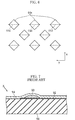
- FIG. 7 shows an example of conventional thermal printhead (see Patent Document 1 given below).
- the illustrated thermal printhead X includes a substrate 91 and a heating resistor element 93 extending on the substrate in the primary scanning direction.
- the heating resistor element 93 is covered by a protective film 94 .
- the heading resistor element 93 is connected to an electrode 92 and another electrode (not shown) whose polarity is opposite to that of the electrode 92 .
- heat is generated.
- the heat is transferred to thermal paper through the protective film 94 , whereby an image or letter is formed on the thermal paper.
- Patent Document 1 JP-A-7-186429
- thermal paper is made smooth.
- surfacing techniques include the application of coating agent to thermal paper.
- the thermal paper having a smooth surface tends to stick to the protective film 94 when pressed against the thermal printhead X.
- sticking occurs, the thermal paper cannot be smoothly slid relative to the thermal printhead X, which may result in deterioration in printing quality.
- the above-described coating agent is generally hydrophilic and tends to absorb moisture in the air.
- the thermal paper is pressed against the protective film 94 , the moisture which has been absorbed in the coating agent may seep out between the thermal paper and the protective film 94 . Conventionally, such moisture also causes the sticking of the thermal paper to the protective film 94 .
- an object of the present invention is to provide a thermal printhead which is capable of preventing sticking.
- a thermal printhead comprising a substrate and a heating resistor element formed on the substrate and elongated in the primary scanning direction.
- the thermal printhead further includes an electrode for applying current to the heating resistor element, and a protective film covering the heating resistor element and the electrode and including a contact surface for coming into contact with a recording medium.
- the contact surface of the protective film is made irregular to reduce contact area with the recording medium.
- the protective film includes a first layer directly covering the heating resistor element and the electrode, a second layer formed on the first layer, and a third layer formed on the second layer to come into contact with the recording medium.
- the first layer is made of glass
- the second layer is made of porous glass including a plurality of pores
- the third layer is made of a water repellent material. The third layer partially enters each of the pores of the second layer.
- the third layer is made of polyimide resin.
- the protective film includes a first layer directly covering the heating resistor element and the electrode and a second layer formed on the first layer.
- the second layer comprises a plurality of projecting elements spaced from each other.
- each of the projecting elements has a rectangular cross section, and a diagonal of the rectangular cross section is parallel to the secondary scanning direction which is perpendicular to the primary scanning direction.
- the protective film includes a third layer covering the second layer and having water repellency.
- the second layer is made of either of SiC and a composite material of C and SiC, whereas the third layer is made of polytetrafluoroethylene.
- FIG. 1 is a perspective view showing a principal portion of a thermal printhead according to a first embodiment of the present invention.
- FIG. 2 is a sectional view taken along lines II-II in FIG. 1 .
- FIG. 3 is a sectional view showing the structure of a protective film of the thermal printhead of the first embodiment.
- FIG. 4 is a perspective view showing a principal portion of a thermal printhead according to a second embodiment of the present invention.
- FIG. 5 is a sectional view taken along lines V-V in FIG. 4 .
- FIG. 6 is a plan view showing projecting elements of the thermal printhead according to the second embodiment.
- FIG. 7 is a sectional view showing a principal portion of a conventional thermal printhead.
- FIGS. 1-3 show a thermal printhead according to a first embodiment of the present invention.
- the illustrated thermal printhead A 1 includes an insulating substrate 1 , electrodes 2 A and 2 B, a heating resistor element 3 and a protective film 4 .
- the heating resistor element 3 is elongated in the primary scanning direction (x direction in FIG. 1 ).
- recording paper such as thermal paper is transferred in the secondary scanning direction (y direction in FIG. 1 ) relative to the thermal printhead A 1 .
- the substrate 1 is made of e.g. a ceramic material.
- a glaze layer (not shown) is formed on the substrate 1 to provide a smooth surface. The glaze layer also functions to prevent heat from escaping from the heating resistor element 3 to the substrate 1 .
- the electrodes 2 A and 2 B are made of a metal such as Au and have different electrical polarities.
- the electrode 2 A includes a plurality of comb-teeth-shaped extensions 21 extending in the secondary scanning direction y, and the electrode 2 B also has similar extensions 22 .
- the extensions 21 and 22 are alternately arranged in the primary scanning direction x.
- the electrodes 2 A and 2 B are connected to a non-illustrated drive IC.
- the electrodes 2 A and 2 B may be formed by printing Au resinate paste into a predetermined shape and then baking the paste.
- the second layer 42 is made of e.g. glass and laminated on the first layer 41 . As shown in FIG. 3 , the second layer 42 has a porous structure including a plurality of pores 42 a .
- the thickness of the second layer 42 is e.g. about 4 to 6 ⁇ m.
- the diameter of the pores 42 a is e.g. about several tens of ⁇ m.
- the second layer 42 may be formed as follows. First, conductive paste is uniformly printed on the first layer 41 .
- the conductive paste use is made of a mixture of glass paste (base paste) containing SiO 2 , ZnO, CaO as the main components and resistor paste.
- the resistor paste is prepared by adding 0.3 to 30 wt % of ruthenium oxide particles having a particle size of about 0.001 to 1 ⁇ m to glass made of e.g. PbO, SiO 2 , B 2 O 3 .
- the softening points of the base paste and the resistor paste are 785° C. and 865° C., respectively.
- the conductive paste is then baked at a temperature of e.g. 760° C. This baking temperature is lower than both of the softening temperature of the base paste and that of the resistor paste. Thus, the conductive paste does not flow considerably during the baking. In the baking process, bubbles are formed around the ruthenium oxide contained in the conductive paste. These bubbles finally form the pores 42 a , whereby the porous second layer 42 is obtained.
- the third layer 43 covers the second layer 42 and portions of the first layer 41 which are not covered by the second layer 42 .
- the third layer 43 is made of e.g. polyimide resin and has water repellency.
- the third layer 43 has a thickness of about 1 to 10 ⁇ m.
- Each pore 42 a of the second layer 42 is filled with the third layer 43 at least partially. Due to the existence of the pores 42 a , the upper surface of the third layer 43 (and hence the protective film 4 ) is not a smooth surface but an irregular surface including recesses 4 a at locations corresponding to the pores 42 a .
- the third layer 43 may be formed by printing or transferring a water-repellent resin onto the second layer 42 .
- thermal printhead A 1 The advantages of the thermal printhead A 1 will be described below.
- the moisture is retained in the recesses 4 a .
- the use of polyimide resin, which has water repellency, as the material of the third layer 43 is advantageous for preventing moisture from being retained at the contact portion between the protective film 4 and the thermal paper.
- a material which has an appropriate level of water repellency and provides a smooth surface may be used instead of polyimide resin.
- FIGS. 4-6 show a thermal printhead according to a second embodiment of the present invention.
- the elements which are identical or similar to those of the first embodiment are designated by the same reference signs as those used for FIGS. 1-3 .
- the third layer 45 covers the second layer 44 (i.e., the projecting elements 44 a ) and the upper surface of the first layer 41 (the portions which are not covered by the projecting elements 44 a ).
- the third layer 45 fills only part of the space between adjacent projecting elements 44 a and does not fill the space completely. Thus, the surface (which is to come into contact with paper) of the protective film 4 is irregular.
- the third layer 45 is made of e.g. polytetrafluoroethylene (hereinafter referred to as “PTFE”) and has water repellency.
- the thickness of the third layer 45 is e.g. about 2 to 3 ⁇ m.
- the third layer 45 may be formed by e.g. printing, transferring or sputtering.
- each projecting element 44 a is parallel to the secondary scanning direction y, and any side of the rectangular cross section is not parallel to the primary scanning direction x.
- the projecting element 44 a comes into contact (via the third layer 45 ) with the thermal paper, which is being transferred in the secondary scanning direction y, from its apex. This is suitable for achieving smooth feed of the thermal paper.
- the second layer 44 is made of SiC or C—SiC
- the carbon content is relatively large.
- the third layer 45 strongly adheres to the second layer 44 .
- SiC and C—SiC has a high thermal conductivity, the heat from the heating resistor element 3 is efficiently transferred to the thermal paper.
- the third layer 45 of the protective film 4 according to the second embodiment can be eliminated. In this case, the projecting elements 44 a constituting the second layer 44 directly come into contact with the thermal paper.
- the formation density of the projecting elements 44 a i.e., the number of projecting elements per unit area
- the thermal paper is not damaged by the projecting elements 44 a when the paper is being transferred.
- any of the projecting elements 42 a has a defect (e.g. breakage or release from the first layer 41 ), it does not have an adverse effect on other projecting elements 42 a.
- the projecting elements 44 a are not limited to those having a rectangular cross section. For instance, projecting elements which are polygonal or circular in cross section may be employed.
- the materials of the second layer 44 and the third layer 45 are not limited to those described above.
- the second layer 44 may be made of silane coupler
- the third layer 45 may be made of polyimide resin.
- the third layer 45 made of polyimide resin exhibits good water repellency and achieves smooth sliding relative to the thermal paper. Polyimide resin and silane coupler can be bonded strongly to each other.
Landscapes
- Electronic Switches (AREA)
Abstract
Description
Claims (6)
Applications Claiming Priority (5)
| Application Number | Priority Date | Filing Date | Title |
|---|---|---|---|
| JP2006-171267 | 2006-06-21 | ||
| JP2006171267A JP2008000947A (en) | 2006-06-21 | 2006-06-21 | Thermal printing head |
| JP2006-172346 | 2006-06-22 | ||
| JP2006172346A JP2008000977A (en) | 2006-06-22 | 2006-06-22 | Thermal printing head |
| PCT/JP2007/062263 WO2007148663A1 (en) | 2006-06-21 | 2007-06-19 | Thermal printhead |
Publications (2)
| Publication Number | Publication Date |
|---|---|
| US20090174757A1 US20090174757A1 (en) | 2009-07-09 |
| US7903132B2 true US7903132B2 (en) | 2011-03-08 |
Family
ID=38833405
Family Applications (1)
| Application Number | Title | Priority Date | Filing Date |
|---|---|---|---|
| US12/305,290 Expired - Fee Related US7903132B2 (en) | 2006-06-21 | 2007-06-19 | Thermal printhead |
Country Status (3)
| Country | Link |
|---|---|
| US (1) | US7903132B2 (en) |
| EP (1) | EP2030795A1 (en) |
| WO (1) | WO2007148663A1 (en) |
Families Citing this family (4)
| Publication number | Priority date | Publication date | Assignee | Title |
|---|---|---|---|---|
| WO2005123400A1 (en) * | 2004-06-15 | 2005-12-29 | Rohm Co., Ltd. | Thermal head and manufacturing method thereof |
| JP6661678B2 (en) * | 2018-02-23 | 2020-03-11 | 三菱電機株式会社 | Thermal detection sensor |
| JP7128901B2 (en) | 2018-09-27 | 2022-08-31 | 京セラ株式会社 | thermal printer |
| CN114379239B (en) * | 2021-07-16 | 2023-05-30 | 山东华菱电子股份有限公司 | Heating substrate for thermal printing head with surface resistant to paper dust accumulation and manufacturing method thereof |
Citations (10)
| Publication number | Priority date | Publication date | Assignee | Title |
|---|---|---|---|---|
| JPS62193845A (en) | 1986-02-20 | 1987-08-26 | Fujitsu Ltd | Thermal head |
| US4835550A (en) * | 1987-03-06 | 1989-05-30 | Hitachi, Ltd. | Thick film type thermal head |
| JPH07186429A (en) | 1993-12-28 | 1995-07-25 | Rohm Co Ltd | Manufacture of thermal print head |
| JP2000141729A (en) | 1998-11-11 | 2000-05-23 | Tdk Corp | Thermal head |
| US6236423B1 (en) * | 1999-05-31 | 2001-05-22 | Aoi Electronics Company Limited | Thermal head and method of manufacturing the same |
| JP2002103661A (en) | 2000-09-27 | 2002-04-09 | Kyocera Corp | Thermal printer |
| US6445402B1 (en) * | 1999-03-04 | 2002-09-03 | Fuji Photo Film Co., Ltd. | Contact type recording head and image forming apparatus using the recording head |
| JP2002370397A (en) | 2001-06-13 | 2002-12-24 | Sii P & S Inc | Thermal head |
| WO2005105462A1 (en) | 2004-04-30 | 2005-11-10 | Rohm Co., Ltd. | Thermal print head |
| US20100066798A1 (en) * | 2007-03-15 | 2010-03-18 | Takumi Yamade | Thermal print head |
-
2007
- 2007-06-19 US US12/305,290 patent/US7903132B2/en not_active Expired - Fee Related
- 2007-06-19 WO PCT/JP2007/062263 patent/WO2007148663A1/en active Application Filing
- 2007-06-19 EP EP07767153A patent/EP2030795A1/en not_active Withdrawn
Patent Citations (11)
| Publication number | Priority date | Publication date | Assignee | Title |
|---|---|---|---|---|
| JPS62193845A (en) | 1986-02-20 | 1987-08-26 | Fujitsu Ltd | Thermal head |
| US4835550A (en) * | 1987-03-06 | 1989-05-30 | Hitachi, Ltd. | Thick film type thermal head |
| JPH07186429A (en) | 1993-12-28 | 1995-07-25 | Rohm Co Ltd | Manufacture of thermal print head |
| JP2000141729A (en) | 1998-11-11 | 2000-05-23 | Tdk Corp | Thermal head |
| US6445402B1 (en) * | 1999-03-04 | 2002-09-03 | Fuji Photo Film Co., Ltd. | Contact type recording head and image forming apparatus using the recording head |
| US6236423B1 (en) * | 1999-05-31 | 2001-05-22 | Aoi Electronics Company Limited | Thermal head and method of manufacturing the same |
| JP2002103661A (en) | 2000-09-27 | 2002-04-09 | Kyocera Corp | Thermal printer |
| JP2002370397A (en) | 2001-06-13 | 2002-12-24 | Sii P & S Inc | Thermal head |
| WO2005105462A1 (en) | 2004-04-30 | 2005-11-10 | Rohm Co., Ltd. | Thermal print head |
| US7443409B2 (en) | 2004-04-30 | 2008-10-28 | Rohm Co., Ltd. | Thermal printhead |
| US20100066798A1 (en) * | 2007-03-15 | 2010-03-18 | Takumi Yamade | Thermal print head |
Also Published As
| Publication number | Publication date |
|---|---|
| WO2007148663A1 (en) | 2007-12-27 |
| EP2030795A1 (en) | 2009-03-04 |
| US20090174757A1 (en) | 2009-07-09 |
Similar Documents
| Publication | Publication Date | Title |
|---|---|---|
| US20120147118A1 (en) | Thermal print head | |
| US7903132B2 (en) | Thermal printhead | |
| KR100809823B1 (en) | Thermal print head | |
| CN1968820B (en) | Thermal head and manufacturing method thereof | |
| US20100085412A1 (en) | Thermal print head | |
| JP2008000947A (en) | Thermal printing head | |
| US8009185B2 (en) | Thermal head with protective layer | |
| US6469724B1 (en) | Thick-film thermal print head and its manufacturing method | |
| KR100888521B1 (en) | Thermal head and manufacturing method thereof | |
| US11279145B2 (en) | Thermal print head and method of manufacturing the same | |
| US20090201356A1 (en) | Thermal print head and method for manufacturing the same | |
| US20070296797A1 (en) | Thermal Print Head and Method for Manufacturing Same | |
| JP4163921B2 (en) | Thermal head and thermal printer using the same | |
| US20160332456A1 (en) | Thermal print head | |
| US6512532B2 (en) | Thermal printhead, heating resistor used for the same, and process of making heating resistor | |
| JP2664807B2 (en) | Manufacturing method of thick film thermal head | |
| JP3472755B2 (en) | Thermal head and method of manufacturing the same | |
| JP3051469B2 (en) | Thermal head and method of manufacturing the same | |
| JP4766726B2 (en) | Manufacturing method of thermal head | |
| JP2965339B2 (en) | Manufacturing method of thermal head | |
| JPH06191075A (en) | Thermal head | |
| JP2015189066A (en) | Manufacturing method of thermal head | |
| JPH10272797A (en) | Thermal head | |
| JP2005313591A (en) | Thermal head and thermal printer using the same | |
| JP2000246929A (en) | Manufacture of thermal head |
Legal Events
| Date | Code | Title | Description |
|---|---|---|---|
| AS | Assignment |
Owner name: ROHM CO., LTD., JAPAN Free format text: ASSIGNMENT OF ASSIGNORS INTEREST;ASSIGNORS:SAKO, TERUHISA;KANEI, NAOFUMI;REEL/FRAME:021999/0878 Effective date: 20081008 |
|
| FEPP | Fee payment procedure |
Free format text: PAYOR NUMBER ASSIGNED (ORIGINAL EVENT CODE: ASPN); ENTITY STATUS OF PATENT OWNER: LARGE ENTITY |
|
| STCF | Information on status: patent grant |
Free format text: PATENTED CASE |
|
| FPAY | Fee payment |
Year of fee payment: 4 |
|
| MAFP | Maintenance fee payment |
Free format text: PAYMENT OF MAINTENANCE FEE, 8TH YEAR, LARGE ENTITY (ORIGINAL EVENT CODE: M1552); ENTITY STATUS OF PATENT OWNER: LARGE ENTITY Year of fee payment: 8 |
|
| FEPP | Fee payment procedure |
Free format text: MAINTENANCE FEE REMINDER MAILED (ORIGINAL EVENT CODE: REM.); ENTITY STATUS OF PATENT OWNER: LARGE ENTITY |
|
| LAPS | Lapse for failure to pay maintenance fees |
Free format text: PATENT EXPIRED FOR FAILURE TO PAY MAINTENANCE FEES (ORIGINAL EVENT CODE: EXP.); ENTITY STATUS OF PATENT OWNER: LARGE ENTITY |
|
| STCH | Information on status: patent discontinuation |
Free format text: PATENT EXPIRED DUE TO NONPAYMENT OF MAINTENANCE FEES UNDER 37 CFR 1.362 |
|
| FP | Lapsed due to failure to pay maintenance fee |
Effective date: 20230308 |