US7864154B2 - Gate driving circuit for liquid crystal display device and method of driving the same - Google Patents
Gate driving circuit for liquid crystal display device and method of driving the same Download PDFInfo
- Publication number
- US7864154B2 US7864154B2 US11/646,466 US64646606A US7864154B2 US 7864154 B2 US7864154 B2 US 7864154B2 US 64646606 A US64646606 A US 64646606A US 7864154 B2 US7864154 B2 US 7864154B2
- Authority
- US
- United States
- Prior art keywords
- shift register
- pull
- gate driving
- node
- register stage
- Prior art date
- Legal status (The legal status is an assumption and is not a legal conclusion. Google has not performed a legal analysis and makes no representation as to the accuracy of the status listed.)
- Expired - Fee Related, expires
Links
Images


Classifications
-
- G—PHYSICS
- G09—EDUCATION; CRYPTOGRAPHY; DISPLAY; ADVERTISING; SEALS
- G09G—ARRANGEMENTS OR CIRCUITS FOR CONTROL OF INDICATING DEVICES USING STATIC MEANS TO PRESENT VARIABLE INFORMATION
- G09G3/00—Control arrangements or circuits, of interest only in connection with visual indicators other than cathode-ray tubes
- G09G3/20—Control arrangements or circuits, of interest only in connection with visual indicators other than cathode-ray tubes for presentation of an assembly of a number of characters, e.g. a page, by composing the assembly by combination of individual elements arranged in a matrix no fixed position being assigned to or needed to be assigned to the individual characters or partial characters
- G09G3/34—Control arrangements or circuits, of interest only in connection with visual indicators other than cathode-ray tubes for presentation of an assembly of a number of characters, e.g. a page, by composing the assembly by combination of individual elements arranged in a matrix no fixed position being assigned to or needed to be assigned to the individual characters or partial characters by control of light from an independent source
- G09G3/36—Control arrangements or circuits, of interest only in connection with visual indicators other than cathode-ray tubes for presentation of an assembly of a number of characters, e.g. a page, by composing the assembly by combination of individual elements arranged in a matrix no fixed position being assigned to or needed to be assigned to the individual characters or partial characters by control of light from an independent source using liquid crystals
- G09G3/3611—Control of matrices with row and column drivers
- G09G3/3674—Details of drivers for scan electrodes
- G09G3/3677—Details of drivers for scan electrodes suitable for active matrices only
-
- G—PHYSICS
- G09—EDUCATION; CRYPTOGRAPHY; DISPLAY; ADVERTISING; SEALS
- G09G—ARRANGEMENTS OR CIRCUITS FOR CONTROL OF INDICATING DEVICES USING STATIC MEANS TO PRESENT VARIABLE INFORMATION
- G09G3/00—Control arrangements or circuits, of interest only in connection with visual indicators other than cathode-ray tubes
- G09G3/20—Control arrangements or circuits, of interest only in connection with visual indicators other than cathode-ray tubes for presentation of an assembly of a number of characters, e.g. a page, by composing the assembly by combination of individual elements arranged in a matrix no fixed position being assigned to or needed to be assigned to the individual characters or partial characters
- G09G3/34—Control arrangements or circuits, of interest only in connection with visual indicators other than cathode-ray tubes for presentation of an assembly of a number of characters, e.g. a page, by composing the assembly by combination of individual elements arranged in a matrix no fixed position being assigned to or needed to be assigned to the individual characters or partial characters by control of light from an independent source
- G09G3/36—Control arrangements or circuits, of interest only in connection with visual indicators other than cathode-ray tubes for presentation of an assembly of a number of characters, e.g. a page, by composing the assembly by combination of individual elements arranged in a matrix no fixed position being assigned to or needed to be assigned to the individual characters or partial characters by control of light from an independent source using liquid crystals
-
- G—PHYSICS
- G02—OPTICS
- G02F—OPTICAL DEVICES OR ARRANGEMENTS FOR THE CONTROL OF LIGHT BY MODIFICATION OF THE OPTICAL PROPERTIES OF THE MEDIA OF THE ELEMENTS INVOLVED THEREIN; NON-LINEAR OPTICS; FREQUENCY-CHANGING OF LIGHT; OPTICAL LOGIC ELEMENTS; OPTICAL ANALOGUE/DIGITAL CONVERTERS
- G02F1/00—Devices or arrangements for the control of the intensity, colour, phase, polarisation or direction of light arriving from an independent light source, e.g. switching, gating or modulating; Non-linear optics
- G02F1/01—Devices or arrangements for the control of the intensity, colour, phase, polarisation or direction of light arriving from an independent light source, e.g. switching, gating or modulating; Non-linear optics for the control of the intensity, phase, polarisation or colour
- G02F1/13—Devices or arrangements for the control of the intensity, colour, phase, polarisation or direction of light arriving from an independent light source, e.g. switching, gating or modulating; Non-linear optics for the control of the intensity, phase, polarisation or colour based on liquid crystals, e.g. single liquid crystal display cells
- G02F1/133—Constructional arrangements; Operation of liquid crystal cells; Circuit arrangements
-
- G—PHYSICS
- G09—EDUCATION; CRYPTOGRAPHY; DISPLAY; ADVERTISING; SEALS
- G09G—ARRANGEMENTS OR CIRCUITS FOR CONTROL OF INDICATING DEVICES USING STATIC MEANS TO PRESENT VARIABLE INFORMATION
- G09G3/00—Control arrangements or circuits, of interest only in connection with visual indicators other than cathode-ray tubes
- G09G3/20—Control arrangements or circuits, of interest only in connection with visual indicators other than cathode-ray tubes for presentation of an assembly of a number of characters, e.g. a page, by composing the assembly by combination of individual elements arranged in a matrix no fixed position being assigned to or needed to be assigned to the individual characters or partial characters
-
- G—PHYSICS
- G11—INFORMATION STORAGE
- G11C—STATIC STORES
- G11C19/00—Digital stores in which the information is moved stepwise, e.g. shift registers
- G11C19/28—Digital stores in which the information is moved stepwise, e.g. shift registers using semiconductor elements
-
- G—PHYSICS
- G09—EDUCATION; CRYPTOGRAPHY; DISPLAY; ADVERTISING; SEALS
- G09G—ARRANGEMENTS OR CIRCUITS FOR CONTROL OF INDICATING DEVICES USING STATIC MEANS TO PRESENT VARIABLE INFORMATION
- G09G2300/00—Aspects of the constitution of display devices
- G09G2300/04—Structural and physical details of display devices
- G09G2300/0404—Matrix technologies
- G09G2300/0417—Special arrangements specific to the use of low carrier mobility technology
-
- G—PHYSICS
- G09—EDUCATION; CRYPTOGRAPHY; DISPLAY; ADVERTISING; SEALS
- G09G—ARRANGEMENTS OR CIRCUITS FOR CONTROL OF INDICATING DEVICES USING STATIC MEANS TO PRESENT VARIABLE INFORMATION
- G09G2320/00—Control of display operating conditions
- G09G2320/04—Maintaining the quality of display appearance
- G09G2320/043—Preventing or counteracting the effects of ageing
Definitions
- the present invention relates to a liquid crystal display (LCD) device, and more particularly, to a gate driving circuit for an LCD device and a method of driving the LCD device using the same.
- LCD liquid crystal display
- liquid crystal display (LCD) devices are widely used as monitors for notebook computers and desktop computers because of their excellent characteristics, such as light weight, portability and low power consumption.
- LCD liquid crystal display
- active matrix type LCD devices having thin film transistors (TFTs) as switching elements are actively researched and developed because of their superiority in displaying moving images.
- FIG. 1 is a schematic block diagram of a liquid crystal display device according to the related art
- FIG. 2 is a schematic view showing a liquid crystal display panel of the liquid crystal display device according to the related art.
- the liquid crystal display device includes a liquid crystal display panel 2 and a liquid crystal module (LCM) driving circuit 26 .
- the LCM driving circuit 26 includes an interface 10 , a timing controller 12 , a source voltage generator 14 , a reference voltage generator 16 , a data driver 18 and a gate driver 20 .
- RGB data and timing sync signals such as clock signals, horizontal sync signals, vertical sync signals and data enable signals, are input from an external driving system such as a personal computer to the interface 10 .
- the interface 10 outputs the RGB data and the timing sync signals to the timing controller 12 .
- a low voltage differential signal (LVDS) interface and transistor logic (TTL) interface may be used for transmission of the RGB data and the timing sync signals.
- the interface 10 may be integrated in a single chip together with the timing controller 12 .
- a plurality of gate lines “GL 1 ” to “GLn” and a plurality of data lines “DL 1 ” to “DLm” are formed in the liquid crystal display panel 2 and are driven respectively by the gate driver 20 and the data driver 18 .
- the plurality of gate lines “GL 1 ” to “GLn” and the plurality of data lines “DL 1 ” to “DLm” cross each other to define a plurality of pixel regions.
- a thin film transistor “TFT” is connected to the corresponding gate line and the corresponding data line, and a liquid crystal capacitor “LC” connected to the thin film transistor “TFT” is formed in each pixel region.
- the liquid crystal capacitor “LC” is turned on/off by the thin film transistor “TFT” to thereby modulate the transmittance of incident light through the pixel regions to display images.
- the timing controller 12 generates data control signals for the data driver 18 that includes a plurality of data integrated circuits (ICs), and gate control signals for the gate driver 20 that includes a plurality of gate ICs. Moreover, the timing controller 12 outputs data signals to the data driver 18 .
- the reference voltage generator 16 generates reference voltages using a digital-to-analog converter (DAC) in the data driver 18 . The reference voltages are set up according to transmittance-voltage characteristics of the liquid crystal display panel 2 .
- the data driver 18 determines the reference voltages for the data signals according to the data control signals and outputs the determined reference voltages to the liquid crystal display panel 2 to control a rotation angle of liquid crystal molecules of the liquid crystal capacitors.
- the gate driver 20 controls the ON/OFF operation of the thin film transistors (TFTs) in the liquid crystal display panel 2 according to the gate control signals from the timing controller 12 .
- the gate driver 20 sequentially enables the plurality of gate lines “GL 1 ” to “GLn.” Accordingly, the data signals from the data driver 18 are supplied to the pixels in the pixel regions of the liquid crystal display panel 2 through the TFTs.
- the source voltage generator 14 supplies source voltages to elements of the LCD device and a common voltage to the liquid crystal display panel 2 .
- the liquid crystal display device includes a backlight assembly including at least one lamp.
- the backlight assembly emits light onto the liquid crystal display panel 2 .
- FIG. 3 is a schematic block diagram showing the gate driver of FIG. 1 according to the related art.
- the gate driver 20 includes a plurality of related art shift register stages “SR 1 ” to “SRn”. Each high level voltage (VDD), each low level voltage (VSS) and each clock signal (CLKs) are supplied to each shift register stage “SR 1 ” to “SRn”. Moreover, a start voltage “Vst” is supplied to a first shift register stage “SR 1 ”. The first shift register stage “SR 1 ” outputs a first gate signal “Vg 1 ” to a first gate line (of FIG. 2 ).
- the first gate signal “Vg 1 ” output by the first shift register stage is provided as a start voltage of a second shift register “SR 2 ”.
- the second shift register “SR 2 ” outputs a second gate signal “Vg 2 ” to a second gate line (of FIG. 2 ) in response to the first gate signal “Vg 1 ” output by the first shift register stage.
- the plurality of shift registers “SR 1 ” to “SRn” sequentially supply a plurality of gate signals “Vg 1 ” to “Vgn” to a plurality of gate lines “GL 1 ” to “GLn” as shown in FIG. 4 .
- FIG. 4 is a timing chart showing gate signals of the gate driver according to the related art.
- the plurality of related art shift register stages “SR 1 ” to “SRn” (of FIG. 3 ) sequentially supply the gate signals “Vg 1 ” to “Vg 5 ” respectively to the gate lines “GL 1 ” to “GL 5 ”.
- a plurality of pixel TFTs “TFT” (of FIG. 2 ) connected to the plurality of gate lines “GL 1 ” to “GL 5 ” respectively, are sequentially turned on.
- Each shift register stage “SR 1 ” to “SRn” includes identical elements. As shown in FIG. 5 , each of the shift register stages “SR 1 ” to “SRn” includes pull-up and pull-down TFTs Tup and Tdn.
- the pull-up and pull-down TFTs Tup and Tdn each include an amorphous silicon layer as a semiconductor layer. If the pull-down TFT Tdn is driven under the high voltage for a long period of time, the pull-down TFT Tdn may be damaged.
- the present invention is directed to a gate driving circuit for a liquid crystal display device and a method of driving the same that substantially obviates one or more of the problems due to limitations and disadvantages of the related art.
- An advantage of the present invention is to provide a gate driving circuit for an LCD device that is capable of preventing a pull-down transistor from being damaged.
- a gate driving circuit for a liquid crystal display (LCD) device includes a plurality of shift register stages each including pull-up and pull-down transistors, wherein each of the pull-up and pull-down transistors is connected to a gate driving signal output terminal and controlled by voltages on first and second nodes, respectively, and wherein the pull-down transistors of a (2n ⁇ 1)th shift register stage and a (2)th shift register stage are connected to each other; and a control signal generating unit alternately supplying one of first and second control signals to the pull-down transistors of the (2n ⁇ 1)th and (2n)th shift register stages and the other of the first and second control signals to the pull-down transistors of the (2n+1)th and (2n+2)th shift register stages, wherein n is an integer.
- a method of driving a gate driving circuit for a liquid crystal display (LCD) device including a plurality of shift register stages each including pull-up and pull-down transistors, wherein each of the pull-up and pull-down transistors is connected to a gate driving signal output terminal and each of the pull-up and pull-down transistors is controlled by voltages on first and second nodes, respectively, includes alternately supplying one of first and second control signals to the pull-down transistors of a (2n ⁇ 1)th shift register stage and a (2n)th shift register stage and supplying the other of the first and second control signals to the pull-down transistors of a (2n ⁇ 2)th shift register stage and a (2n ⁇ 3)th shift register stage, wherein the pull-down transistors of the (2n ⁇ 1)th and (2n)th shift register stages are connected to each other and wherein n is a positive integer.
- FIG. 1 is a schematic block diagram of a liquid crystal display device according to the related art.
- FIG. 2 is a schematic view showing a liquid crystal display panel of the liquid crystal display device according to the related art.
- FIG. 3 is a schematic block diagram showing the gate driver of FIG. 1 according to the related art.
- FIG. 4 is a timing chart showing gate signals of the gate driver of FIG. 3 according to the related art.
- FIG. 5 is a circuit diagram of a shift register stage according to the related art.
- FIG. 6 is a schematic block diagram showing the gate driver according to an embodiment of the present invention.
- FIG. 7 is a circuit diagram of shift register stages according to an embodiment of the present invention.
- FIG. 8 is a timing chart showing gate signals of the gate driver of FIG. 6 for driving a liquid crystal display device.
- FIG. 6 is a schematic block diagram showing the gate driver according to an embodiment of the present invention.
- the gate driver includes a stage unit 50 and a control signal supplying unit 60 .
- the stage unit 50 includes a plurality of shift register stages “ST 1 ” to “STn”, and the control signal supplying unit 60 supplies first and second control signals CNT 1 and CNT 2 .
- Each shift register stage “ST 1 ” to “STn” includes a shift register circuit.
- a first shift register stage “ST 1 ” receives a first start voltage Vst with the high level voltage (VDD), the low level voltage (VCC) and the clock signal (CLKs) to thereby output the first gate signal Vg 1 .
- the first gate signal Vg 1 is used as a start voltage of a second shift register “ST 2 ”.
- the second shift register “ST 2 ” outputs a second gate signal “Vg 2 ” to a second gate line in response to first gate signal Vg 1 as a start voltage.
- the plurality of shift registers “ST 1 ” to “STn” sequentially supply a plurality gate signals “Vg 1 ” to “Vgn” to a plurality of gate lines “GL 1 ” to “GLn”.
- the control signal supplying unit 60 functions to prevent the pull-down TFT “TFT” from being damaged. To accomplish this result, the control signal supplying unit 60 alternately supplies the first and second control signals CNT 1 and CNT 2 to two pull-down TFTs “Tdn” of a pair of coupled shift register stages.
- the coupled shift register stages include (2N ⁇ 1)th and (2N)th shift register stages among the plurality of shift register stages “ST 1 ” to “STn”.
- the second control signal CNT 2 is supplied to the third and fourth shift register stages “ST 3 ” and “ST 4 ”.
- the first control signal CNT 1 is supplied to the fifth and sixth shift register stages “ST 5 ” and “ST 6 ”
- the second control signal CNT 2 is supplied to the seventh and eighth shift register stages “ST 7 ” and “ST 8 ”.
- the first control signal CNT 1 has a high level signal during one-fourth of a cycle
- the second control signal CNT 2 has a high level signal delayed as much as a half cycle from the first control signal CNT 1 .
- control signal supplying unit 60 supplies the first and second control signals CNT 1 and CNT 2 that support driving of each of the shift register stages “ST 1 ” to “STn” to prevent damaging the pull-down TFT Tdn.
- control signal supplying unit 60 may be integrated with a gate and data control signal generating circuit in the timing controller.
- FIG. 7 is a circuit diagram of shift register stages according to an embodiment of the present invention.
- each of nth and (n+1)th shift register stages “STn” and “Stn+1” includes the pull-up and pull-down TFTs “Tup” and “Tdn”.
- the pull-up TFT “Tup” is connected to a clock signal input terminal “CLKT” and is controlled by a voltage of a Q node “Q”.
- the pull-up TFT “Tup” supplies an nth gate driving signal “Vout(n)” to a gate driving signal output terminal “VN”.
- the pull-down TFT “Tdn” is connected to the gate driving signal output terminal “VN” and a high level voltage input terminal “VSST” and is controlled by a voltage of a QB node “QB”.
- the reference number “Vout(n)” means the nth gate signal “Vgn” (of FIG. 6 ).
- first to third TFT “T 1 ” to “T 3 ” are provided in the nth shift register stage “STn” for electrically charging and discharging of the Q node “Q”.
- Fourth and sixth TFT “T 4 ” to “T 6 ” are disposed in the nth shift register stage “STn” for electrically charging and discharging of the QB node “QB”.
- the first TFT “T 1 ” is connected to the high level voltage input terminal “VDDT” and is controlled by the start signal “Vst” to electrically charge the Q node “Q” with a high level voltage.
- the second TFT “T 2 ” is connected to the Q node “Q” and a low level voltage input terminal “VSST” and is controlled by the voltage of the QB node “QB” to electrically discharge the Q node “Q”.
- the third TFT “T 3 ” is connected to the Q node “Q” and the low level voltage input terminal “VSST” and is controlled by an (n+1)th gate driving signal “Vout(n+1)” of an (n+1)th shift register stage “STn+1” to electrically discharge the Q node “Q”.
- the fourth TFT “T 4 ” is connected to and controlled by the high level voltage input terminal “VDDT” to electrically charge the QB node “QB” to a high level voltage.
- the fifth TFT “T 5 ” is connected to the QB node “QB” and the low level voltage input terminal “VSST” and is controlled by the voltage of the QB node “QB” to electrically discharge the QB node “QB”.
- the sixth TFT “T 6 ” is connected to the QB node “QB” and the low level voltage input terminal “VSST” and is controlled by the start signal “Vst” to electrically discharge the QB node “QB”.
- the pull-down TFTs “Tdn” in the above-mentioned coupled shift register stages “STn” and “Stn+1” are connected to each other. That is, the QB nodes “QB” in the nth and (n+1)the shift register stages “STn” and “STn+1” are connected to each other such that the same first control signal “CNT 1 ” is commonly supplied to the nth and (n+1)th shift register stages “STn” and “STn+1”. Similarly, the QB nodes “QB” in the (n+2) and (n+3) shift register stages “STn+2” and “Stn+3” are connected to each other such that the same second control signal “CNT 2 ” (of FIG. 6 ) is commonly supplied to the (n+2) and (n+3)th shift register stages.
- the first and sixth TFTs “T 1 ” and “T 6 ” of the nth stage each use an (n ⁇ 1)th gate driving signal as the start signal (excluding the first stage which uses Vst as the start signal).
- the first and sixth TFTs “T 1 ” to “T 6 ” may each be of an identical transistor type such as a negative (NMOS) type.
- the gate driver including the shift register, shown in FIG. 7 can prevent a high level voltage from being continuously supplied to the pull-down TFT “Tdn” to prevent damage to the pull-down TFT “Tdn”.
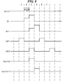
- FIG. 8 is a timing chart showing gate signals of the gate driver for driving a liquid crystal display. Since the nth and (n+1)th shift register stages are driven in a similar manner, the driving process of the nth shift register stage will be explained in detail.
- the Q node “Q” (of FIG. 7 ) of the nth shift register stage “STn” (of FIG. 7 ) is electrically discharged in an initial state.
- the first control signal “CNT 1 ” is supplied the nth shift register stage “STn” (of FIG. 7 ) during one horizontal line period “1H”, as shown in column A.
- the QB node “QB” is electrically charged such that the second transistor “T 2 ” turns on. Accordingly, the Q node “Q” (of FIG.
- the first control signal “CNT 1 ” is supplied to the (n+1)th shift register stage “STn+1” (of FIG. 7 ) such that the Q node “Q” (of FIG. 7 ) of the (n+1)th shift register stage “STn+1” (of FIG. 7 ) is electrically discharged.
- the first and sixth TFTs “T 1 ” (of FIG. 7 ) and “T 6 ” (of FIG. 7 ) turn on in response to the start signal at Vst to electrically charge the Q node “Q” (of FIG. 7 ) using the first TFT “T 1 ” (of FIG. 7 ) and to electrically discharge the QB node “QB” (of FIG. 7 ) using the sixth TFT “T 6 ” (of FIG. 7 ).
- a second pair of coupled shift register stages for example an (n+2)th shift register stage and an (n+3)th shift register stage, is driven to be delayed as much as two horizontal line periods (2H) from the nth and (n+1)th shift register stages “STn” (of FIG. 7 ) and “STn+1” (of FIG. 7 )
- a second control signal “CNT 2 ” is supplied to the QB node “QB” (of FIG. 7 ) in the (n+2)th and (N+3)th shift register stages as much delayed by two horizontal line periods (2H) from the first control signal “CNT 1 ”.
- the (n+2)th and (N+3)th shift register stages are driven using the above-described driving processes with the second control signal “CNT 2 ” used in place of the first control signal “CNT 1 ”.
Abstract
Description
Claims (17)
Applications Claiming Priority (2)
| Application Number | Priority Date | Filing Date | Title |
|---|---|---|---|
| KR1020060053875A KR101252572B1 (en) | 2006-06-15 | 2006-06-15 | Gate driving circuit and driving method thereof for LCD |
| KR10-2006-0053875 | 2006-06-15 |
Publications (2)
| Publication Number | Publication Date |
|---|---|
| US20070290982A1 US20070290982A1 (en) | 2007-12-20 |
| US7864154B2 true US7864154B2 (en) | 2011-01-04 |
Family
ID=38861049
Family Applications (1)
| Application Number | Title | Priority Date | Filing Date |
|---|---|---|---|
| US11/646,466 Expired - Fee Related US7864154B2 (en) | 2006-06-15 | 2006-12-28 | Gate driving circuit for liquid crystal display device and method of driving the same |
Country Status (2)
| Country | Link |
|---|---|
| US (1) | US7864154B2 (en) |
| KR (1) | KR101252572B1 (en) |
Cited By (1)
| Publication number | Priority date | Publication date | Assignee | Title |
|---|---|---|---|---|
| US10255843B2 (en) | 2016-08-29 | 2019-04-09 | Wuhan China Star Optoelectronics Technology Co., Ltd. | Scan driving circuit and flat display device thereof |
Families Citing this family (21)
| Publication number | Priority date | Publication date | Assignee | Title |
|---|---|---|---|---|
| KR101432827B1 (en) * | 2008-04-30 | 2014-08-26 | 엘지디스플레이 주식회사 | liquid crystal display device |
| US7817771B2 (en) * | 2008-12-15 | 2010-10-19 | Au Optronics Corporation | Shift register |
| CN101521043B (en) * | 2009-03-19 | 2011-01-26 | 友达光电股份有限公司 | Shift buffer |
| KR101824074B1 (en) | 2009-06-25 | 2018-01-31 | 가부시키가이샤 한도오따이 에네루기 켄큐쇼 | Display device |
| KR101308474B1 (en) * | 2010-04-19 | 2013-09-16 | 엘지디스플레이 주식회사 | Shift register |
| JP5584148B2 (en) * | 2011-01-25 | 2014-09-03 | 株式会社ジャパンディスプレイ | Gate signal line driving circuit and display device |
| KR102051846B1 (en) * | 2012-07-31 | 2019-12-05 | 삼성디스플레이 주식회사 | Display driving circuit and display device having them |
| KR102050317B1 (en) * | 2013-01-18 | 2019-11-29 | 엘지디스플레이 주식회사 | Gate draving circuit and liquiud crystal display device inculding the same |
| CN103559868A (en) * | 2013-10-12 | 2014-02-05 | 深圳市华星光电技术有限公司 | Grid drive circuit and array substrate and display panel thereof |
| KR102174888B1 (en) | 2014-02-12 | 2020-11-06 | 삼성디스플레이 주식회사 | Gate driving circuit and display device having the same |
| KR102208397B1 (en) * | 2014-08-05 | 2021-01-27 | 엘지디스플레이 주식회사 | Gate driver of display device |
| CN104157259B (en) * | 2014-09-10 | 2016-06-22 | 深圳市华星光电技术有限公司 | Gate driver circuit based on IGZO processing procedure |
| KR20160103616A (en) | 2015-02-24 | 2016-09-02 | 삼성디스플레이 주식회사 | Scan driver |
| KR102343799B1 (en) | 2015-04-02 | 2021-12-28 | 삼성디스플레이 주식회사 | Gate driver and display device including the same |
| CN106531117B (en) | 2017-01-05 | 2019-03-15 | 京东方科技集团股份有限公司 | Shift register, its driving method, grid integrated drive electronics and display device |
| KR102643465B1 (en) | 2017-01-17 | 2024-03-05 | 삼성디스플레이 주식회사 | Display device and driving method thereof |
| CN109064964B (en) * | 2018-09-18 | 2021-11-09 | 合肥鑫晟光电科技有限公司 | Shifting register unit, driving method, grid driving circuit and display device |
| WO2021022548A1 (en) * | 2019-08-08 | 2021-02-11 | 京东方科技集团股份有限公司 | Gate driving unit, circuit, display substrate, display panel and display apparatus |
| CN110459189B (en) * | 2019-08-21 | 2021-10-12 | 京东方科技集团股份有限公司 | Shifting register unit, driving method, grid driving circuit and display device |
| CN115762419A (en) * | 2021-09-03 | 2023-03-07 | 乐金显示有限公司 | Gate driver and display device including the same |
| WO2024065658A1 (en) * | 2022-09-30 | 2024-04-04 | 京东方科技集团股份有限公司 | Gate driving circuit and driving method therefor, and display panel and display apparatus |
Citations (2)
| Publication number | Priority date | Publication date | Assignee | Title |
|---|---|---|---|---|
| US20060049404A1 (en) * | 2004-09-09 | 2006-03-09 | Haeng-Won Park | Transistor and display device having the same |
| US20070086558A1 (en) * | 2005-10-18 | 2007-04-19 | Au Optronics Corporation | Gate line drivers for active matrix displays |
-
2006
- 2006-06-15 KR KR1020060053875A patent/KR101252572B1/en active IP Right Grant
- 2006-12-28 US US11/646,466 patent/US7864154B2/en not_active Expired - Fee Related
Patent Citations (2)
| Publication number | Priority date | Publication date | Assignee | Title |
|---|---|---|---|---|
| US20060049404A1 (en) * | 2004-09-09 | 2006-03-09 | Haeng-Won Park | Transistor and display device having the same |
| US20070086558A1 (en) * | 2005-10-18 | 2007-04-19 | Au Optronics Corporation | Gate line drivers for active matrix displays |
Cited By (1)
| Publication number | Priority date | Publication date | Assignee | Title |
|---|---|---|---|---|
| US10255843B2 (en) | 2016-08-29 | 2019-04-09 | Wuhan China Star Optoelectronics Technology Co., Ltd. | Scan driving circuit and flat display device thereof |
Also Published As
| Publication number | Publication date |
|---|---|
| KR20070119346A (en) | 2007-12-20 |
| US20070290982A1 (en) | 2007-12-20 |
| KR101252572B1 (en) | 2013-04-09 |
Similar Documents
| Publication | Publication Date | Title |
|---|---|---|
| US7864154B2 (en) | Gate driving circuit for liquid crystal display device and method of driving the same | |
| US8339349B2 (en) | Gate driving unit for liquid crystal display device and method of repairing the same | |
| US8344991B2 (en) | Display device and driving method thereof | |
| TWI425771B (en) | Shift register circuit | |
| US7626568B2 (en) | Gate switch apparatus for amorphous silicon LCD | |
| US8289261B2 (en) | Gate driving circuit and display device having the same | |
| US7486268B2 (en) | Gate driving apparatus and method for liquid crystal display | |
| US8344989B2 (en) | Shift register | |
| US8552958B2 (en) | Method of driving a gate line, gate drive circuit for performing the method and display apparatus having the gate drive circuit | |
| US9286846B2 (en) | Liquid crystal display and bidirectional shift register apparatus thereof | |
| US9583059B2 (en) | Level shift circuit, array substrate and display device | |
| US20080211760A1 (en) | Liquid Crystal Display and Gate Driving Circuit Thereof | |
| US20140152629A1 (en) | Shift register and flat panel display device including the same | |
| US20080278467A1 (en) | Liquid crystal display having progressive and interlaced modes, and driving method of the liquid crystal display | |
| JP2010186537A (en) | Shift register driving method, shift register, and liquid crystal display device provided with the same | |
| JP2002258819A (en) | Shift register. liquid crystal display using the same, and method of driving its gate line and data line block | |
| KR20090031052A (en) | Gate diriver and method for driving display apparatus having the smae | |
| KR20080111233A (en) | Driving apparatus for liquid crystal display and liquid crystal display including the same | |
| KR20070013013A (en) | Display device | |
| TWI433081B (en) | Driving circuit for driving liquid crystal display panel | |
| US11276362B2 (en) | TFT array substrate and display panel | |
| CN111048025A (en) | Shift register and display device using the same | |
| KR20080011896A (en) | Gate on voltage generation circuit and gate off voltage generation circuit and liquid crystal display having the same | |
| US8054262B2 (en) | Circuit for stabilizing common voltage of a liquid crystal display device | |
| US7561138B2 (en) | Liquid crystal display device and method of driving the same |
Legal Events
| Date | Code | Title | Description |
|---|---|---|---|
| AS | Assignment |
Owner name: LG.PHILIPS LCD CO., LTD., KOREA, REPUBLIC OF Free format text: ASSIGNMENT OF ASSIGNORS INTEREST;ASSIGNORS:KIM, DO-HEON;MOON, SOO-HWAN;CHAE, JI-EUN;REEL/FRAME:018751/0208 Effective date: 20061218 |
|
| AS | Assignment |
Owner name: LG DISPLAY CO., LTD., KOREA, REPUBLIC OF Free format text: CHANGE OF NAME;ASSIGNOR:LG.PHILIPS LCD CO., LTD.;REEL/FRAME:021763/0177 Effective date: 20080304 Owner name: LG DISPLAY CO., LTD.,KOREA, REPUBLIC OF Free format text: CHANGE OF NAME;ASSIGNOR:LG.PHILIPS LCD CO., LTD.;REEL/FRAME:021763/0177 Effective date: 20080304 |
|
| STCF | Information on status: patent grant |
Free format text: PATENTED CASE |
|
| FEPP | Fee payment procedure |
Free format text: PAYOR NUMBER ASSIGNED (ORIGINAL EVENT CODE: ASPN); ENTITY STATUS OF PATENT OWNER: LARGE ENTITY |
|
| FPAY | Fee payment |
Year of fee payment: 4 |
|
| MAFP | Maintenance fee payment |
Free format text: PAYMENT OF MAINTENANCE FEE, 8TH YEAR, LARGE ENTITY (ORIGINAL EVENT CODE: M1552) Year of fee payment: 8 |
|
| FEPP | Fee payment procedure |
Free format text: MAINTENANCE FEE REMINDER MAILED (ORIGINAL EVENT CODE: REM.); ENTITY STATUS OF PATENT OWNER: LARGE ENTITY |
|
| LAPS | Lapse for failure to pay maintenance fees |
Free format text: PATENT EXPIRED FOR FAILURE TO PAY MAINTENANCE FEES (ORIGINAL EVENT CODE: EXP.); ENTITY STATUS OF PATENT OWNER: LARGE ENTITY |
|
| STCH | Information on status: patent discontinuation |
Free format text: PATENT EXPIRED DUE TO NONPAYMENT OF MAINTENANCE FEES UNDER 37 CFR 1.362 |
|
| FP | Lapsed due to failure to pay maintenance fee |
Effective date: 20230104 |