US7855382B2 - Pixel structure - Google Patents
Pixel structure Download PDFInfo
- Publication number
- US7855382B2 US7855382B2 US12/725,458 US72545810A US7855382B2 US 7855382 B2 US7855382 B2 US 7855382B2 US 72545810 A US72545810 A US 72545810A US 7855382 B2 US7855382 B2 US 7855382B2
- Authority
- US
- United States
- Prior art keywords
- dielectric layer
- gate
- layer
- patterned
- pixel electrode
- Prior art date
- Legal status (The legal status is an assumption and is not a legal conclusion. Google has not performed a legal analysis and makes no representation as to the accuracy of the status listed.)
- Active
Links
Images


Classifications
-
- G—PHYSICS
- G02—OPTICS
- G02F—OPTICAL DEVICES OR ARRANGEMENTS FOR THE CONTROL OF LIGHT BY MODIFICATION OF THE OPTICAL PROPERTIES OF THE MEDIA OF THE ELEMENTS INVOLVED THEREIN; NON-LINEAR OPTICS; FREQUENCY-CHANGING OF LIGHT; OPTICAL LOGIC ELEMENTS; OPTICAL ANALOGUE/DIGITAL CONVERTERS
- G02F1/00—Devices or arrangements for the control of the intensity, colour, phase, polarisation or direction of light arriving from an independent light source, e.g. switching, gating or modulating; Non-linear optics
- G02F1/01—Devices or arrangements for the control of the intensity, colour, phase, polarisation or direction of light arriving from an independent light source, e.g. switching, gating or modulating; Non-linear optics for the control of the intensity, phase, polarisation or colour
- G02F1/13—Devices or arrangements for the control of the intensity, colour, phase, polarisation or direction of light arriving from an independent light source, e.g. switching, gating or modulating; Non-linear optics for the control of the intensity, phase, polarisation or colour based on liquid crystals, e.g. single liquid crystal display cells
- G02F1/133—Constructional arrangements; Operation of liquid crystal cells; Circuit arrangements
- G02F1/1333—Constructional arrangements; Manufacturing methods
- G02F1/1335—Structural association of cells with optical devices, e.g. polarisers or reflectors
- G02F1/133553—Reflecting elements
- G02F1/133555—Transflectors
-
- H—ELECTRICITY
- H01—ELECTRIC ELEMENTS
- H01L—SEMICONDUCTOR DEVICES NOT COVERED BY CLASS H10
- H01L27/00—Devices consisting of a plurality of semiconductor or other solid-state components formed in or on a common substrate
- H01L27/02—Devices consisting of a plurality of semiconductor or other solid-state components formed in or on a common substrate including semiconductor components specially adapted for rectifying, oscillating, amplifying or switching and having at least one potential-jump barrier or surface barrier; including integrated passive circuit elements with at least one potential-jump barrier or surface barrier
- H01L27/12—Devices consisting of a plurality of semiconductor or other solid-state components formed in or on a common substrate including semiconductor components specially adapted for rectifying, oscillating, amplifying or switching and having at least one potential-jump barrier or surface barrier; including integrated passive circuit elements with at least one potential-jump barrier or surface barrier the substrate being other than a semiconductor body, e.g. an insulating body
- H01L27/1214—Devices consisting of a plurality of semiconductor or other solid-state components formed in or on a common substrate including semiconductor components specially adapted for rectifying, oscillating, amplifying or switching and having at least one potential-jump barrier or surface barrier; including integrated passive circuit elements with at least one potential-jump barrier or surface barrier the substrate being other than a semiconductor body, e.g. an insulating body comprising a plurality of TFTs formed on a non-semiconducting substrate, e.g. driving circuits for AMLCDs
- H01L27/124—Devices consisting of a plurality of semiconductor or other solid-state components formed in or on a common substrate including semiconductor components specially adapted for rectifying, oscillating, amplifying or switching and having at least one potential-jump barrier or surface barrier; including integrated passive circuit elements with at least one potential-jump barrier or surface barrier the substrate being other than a semiconductor body, e.g. an insulating body comprising a plurality of TFTs formed on a non-semiconducting substrate, e.g. driving circuits for AMLCDs with a particular composition, shape or layout of the wiring layers specially adapted to the circuit arrangement, e.g. scanning lines in LCD pixel circuits
-
- H—ELECTRICITY
- H01—ELECTRIC ELEMENTS
- H01L—SEMICONDUCTOR DEVICES NOT COVERED BY CLASS H10
- H01L27/00—Devices consisting of a plurality of semiconductor or other solid-state components formed in or on a common substrate
- H01L27/02—Devices consisting of a plurality of semiconductor or other solid-state components formed in or on a common substrate including semiconductor components specially adapted for rectifying, oscillating, amplifying or switching and having at least one potential-jump barrier or surface barrier; including integrated passive circuit elements with at least one potential-jump barrier or surface barrier
- H01L27/12—Devices consisting of a plurality of semiconductor or other solid-state components formed in or on a common substrate including semiconductor components specially adapted for rectifying, oscillating, amplifying or switching and having at least one potential-jump barrier or surface barrier; including integrated passive circuit elements with at least one potential-jump barrier or surface barrier the substrate being other than a semiconductor body, e.g. an insulating body
- H01L27/1214—Devices consisting of a plurality of semiconductor or other solid-state components formed in or on a common substrate including semiconductor components specially adapted for rectifying, oscillating, amplifying or switching and having at least one potential-jump barrier or surface barrier; including integrated passive circuit elements with at least one potential-jump barrier or surface barrier the substrate being other than a semiconductor body, e.g. an insulating body comprising a plurality of TFTs formed on a non-semiconducting substrate, e.g. driving circuits for AMLCDs
- H01L27/1248—Devices consisting of a plurality of semiconductor or other solid-state components formed in or on a common substrate including semiconductor components specially adapted for rectifying, oscillating, amplifying or switching and having at least one potential-jump barrier or surface barrier; including integrated passive circuit elements with at least one potential-jump barrier or surface barrier the substrate being other than a semiconductor body, e.g. an insulating body comprising a plurality of TFTs formed on a non-semiconducting substrate, e.g. driving circuits for AMLCDs with a particular composition or shape of the interlayer dielectric specially adapted to the circuit arrangement
-
- G—PHYSICS
- G02—OPTICS
- G02F—OPTICAL DEVICES OR ARRANGEMENTS FOR THE CONTROL OF LIGHT BY MODIFICATION OF THE OPTICAL PROPERTIES OF THE MEDIA OF THE ELEMENTS INVOLVED THEREIN; NON-LINEAR OPTICS; FREQUENCY-CHANGING OF LIGHT; OPTICAL LOGIC ELEMENTS; OPTICAL ANALOGUE/DIGITAL CONVERTERS
- G02F1/00—Devices or arrangements for the control of the intensity, colour, phase, polarisation or direction of light arriving from an independent light source, e.g. switching, gating or modulating; Non-linear optics
- G02F1/01—Devices or arrangements for the control of the intensity, colour, phase, polarisation or direction of light arriving from an independent light source, e.g. switching, gating or modulating; Non-linear optics for the control of the intensity, phase, polarisation or colour
- G02F1/13—Devices or arrangements for the control of the intensity, colour, phase, polarisation or direction of light arriving from an independent light source, e.g. switching, gating or modulating; Non-linear optics for the control of the intensity, phase, polarisation or colour based on liquid crystals, e.g. single liquid crystal display cells
- G02F1/133—Constructional arrangements; Operation of liquid crystal cells; Circuit arrangements
- G02F1/136—Liquid crystal cells structurally associated with a semi-conducting layer or substrate, e.g. cells forming part of an integrated circuit
- G02F1/1362—Active matrix addressed cells
- G02F1/136227—Through-hole connection of the pixel electrode to the active element through an insulation layer
Definitions
- the invention relates to a pixel structure and a manufacturing method thereof. More particularly, the invention relates to a pixel structure having a reflective pixel electrode and a manufacturing method thereof.
- LCDs liquid crystal displays
- PDAs personal digital assistants
- pocket PCs pocket PCs
- the portable electronic devices not only necessitate satisfactory display performance indoors, but also require appropriate frame qualities outdoors or in a high luminance environment.
- TR-LCD transflective LCD
- a pixel structure is equipped with a reflective pixel electrode suitable for reflecting external light, such that a reflective area is formed.
- a padding layer is frequently inserted under the reflective pixel electrode.
- the TR-LCD having dual cell gap can be constructed.
- a plurality of photoresist bumps is often disposed under the reflective pixel electrode in the conventional pixel structure, so as to improve the reflectivity of the reflective pixel electrode.
- the padding layer, the reflective pixel electrode on the padding layer, and the photoresist bumps are fabricated through a rather complicated process and require more manufacturing costs. Based on the above, it is rather difficult to simplify the process of manufacturing the pixel structure of the TR-LCD while a reduced cost and a desirable quality of the pixel structure are needed to be guaranteed.
- the invention is directed to a pixel structure capable of implementing a single cell gap process to fabricate a TR-LCD.
- the invention is further directed to a manufacturing method of a pixel structure for fabricating the pixel structure with higher reflectivity and better quality through performing a simplified manufacturing process.
- the invention provides a pixel structure suitable for being disposed on a substrate.
- the pixel structure includes a gate, a gate dielectric layer, a patterned semiconductor layer, a patterned dielectric layer, a patterned metal layer, an overcoat dielectric layer, and a transparent pixel electrode.
- the gate is disposed on the substrate on which the patterned dielectric layer is disposed to cover the gate.
- the patterned semiconductor layer is disposed on the gate dielectric layer and has a channel area located above the gate.
- the patterned dielectric layer is disposed on the patterned semiconductor layer and has an etching-stop layer disposed above the gate and a plurality of bumps.
- the patterned metal layer includes a source, a drain and a reflective pixel electrode connected to the drain.
- the source and the drain respectively cover portions of the channel area, while the reflective pixel electrode covers the bumps to form an uneven surface.
- the gate, the gate dielectric layer, the patterned semiconductor layer, the source, and the drain together form a transistor.
- the overcoat dielectric layer is disposed on the transistor and includes a contact opening to expose a portion of the reflective pixel electrode.
- the transparent pixel electrode is disposed on the overcoat dielectric layer and is electrically connected to the reflective pixel electrode through the contact opening.
- the pixel structure further includes an ohmic contact layer sandwiched between the patterned metal layer and the patterned semiconductor layer and between the patterned metal layer and the patterned dielectric layer.
- the ohmic contact layer and the patterned metal layer have identical patterns.
- a dielectric constant of the overcoat dielectric layer approximately ranges from 2 to 7.
- a thickness of the overcoat dielectric layer approximately ranges from 0.1 ⁇ m to 6 ⁇ m.
- a thickness of the bumps approximately ranges from 0.1 ⁇ m to 3 ⁇ m.
- the pixel structure further includes a common electrode line disposed on the substrate.
- the common electrode line and a portion of the reflective pixel electrode disposed above the common electrode line together form a storage capacitor.
- the bumps include organic bumps or inorganic bumps.
- the invention further provides a manufacturing method of a pixel structure.
- the manufacturing method includes following steps. First, a substrate is provided, and a gate is formed on the substrate. Next, a gate dielectric layer is formed on the substrate and covers the gate. Thereafter, a semiconductor layer is formed on the gate dielectric layer and has a channel area located above the gate. A patterned dielectric layer is then formed on the semiconductor layer and includes an etching-stop layer disposed above the gate and a plurality of bumps. After that, a patterned metal layer is formed over the substrate and includes a source, a drain and a reflective pixel electrode connected to the drain. The source and the drain respectively cover portions of the channel area. The reflective pixel electrode covers the bumps to form an uneven surface.
- the semiconductor layer is patterned with use of the patterned metal layer as a mask, so as to form a patterned semiconductor layer.
- the gate, the gate dielectric layer, the patterned semiconductor layer, the source and the drain together form a transistor.
- an overcoat dielectric layer is formed on the transistor, and a contact opening is formed on the overcoat dielectric layer to expose a portion of the reflective pixel electrode.
- a transparent pixel electrode is formed on the overcoat dielectric layer and is electrically connected to the reflective pixel electrode through the contact opening.
- the manufacturing method further includes forming an ohmic contact layer sandwiched between the patterned metal layer and the patterned semiconductor layer and between the patterned metal layer and the patterned dielectric layer.
- the ohmic contact layer and the patterned metal layer are patterned simultaneously.
- a dielectric constant of the overcoat dielectric layer approximately ranges from 2 to 7.
- a thickness of the overcoat dielectric layer approximately ranges from 0.1 ⁇ m to 6 ⁇ m.
- a thickness of the bumps approximately ranges from 0.1 ⁇ m to 3 ⁇ m.
- a common electrode line is further formed on the substrate when the gate is formed.
- the common electrode line and a portion of the reflective pixel electrode disposed above the common electrode line together form a storage capacitor.
- the plurality of bumps is formed during the formation of the etching-stop layer.
- the reflective pixel electrode covers the bumps.
- the overcoat dielectric layer covers the reflective pixel electrode, so as to adjust an electrical field above the reflective pixel electrode.
- FIGS. 1A through 1E are top views depicting a manufacturing method of a pixel structure according to an embodiment of the invention.
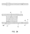
- FIGS. 2A through 2E are cross-sectional views along lines A-A′ and B-B′ of FIGS. 1A through 1E .
- FIG. 3 is a cross-sectional view of a pixel structure according to another embodiment of the invention.
- a reflective pixel electrode disposed in a pixel structure enables the pixel structure to reflect lights.
- a transparent pixel electrode is simultaneously disposed outside the reflective pixel electrode in the pixel structure, the pixel structure is able to display both in a transmissive mode and in a reflective mode.
- a padding layer inserted under the reflective pixel electrode and photoresist bumps for increasing the reflectivity of the pixel structure are often fabricated in the pixel structure to ensure the display quality thereof.
- said process complicates the fabrication of the pixel structure, leading to a reduction in production and yield of the products.
- the invention provides a manufacturing method of a pixel structure for fabricating the pixel structure with great quality in a simplified manufacturing process.
- FIGS. 1A through 1E are top views depicting a manufacturing method of a pixel structure according to an embodiment of the invention.
- FIGS. 2A through 2E are cross-sectional views along lines A-A′ and B-B′ of FIGS. 1A through 1E .
- a method of forming the gate 120 includes, for example, forming a gate material layer (not shown) on the substrate 110 through performing a sputtering process and then patterning the gate material layer through implementing an etching process with use of a patterned photoresist as a mask, such that the gate 120 is formed.
- a common electrode line CL, a scan line SL connected to the gate 120 , and a bonding pad P for drivers can be together formed on the substrate 110 .
- the substrate 110 may be a transparent substrate such as a glass substrate, a plastic substrate, and so forth, and the material of the gate material layer may be either any conductive material applied to fabricate the gate 120 in the related technical field or a combination of various conductive materials.
- the material of the gate material layer can be aluminum (Al), copper (Cu), molybdenum (Mo), silver (Ag), gold (Au), an alloy consisting of said metals, or a composite metal layer consisting of said metals.
- a gate dielectric layer 130 and a semiconductor layer 140 are sequentially formed on the substrate 110 .
- the gate dielectric layer 130 covers the gate 120 , the common electrode line CL, the scan line SL and the bonding pad P, while and the semiconductor layer 140 covers the gate dielectric layer 130 and includes a channel area 142 located above the gate 120 .
- a patterned dielectric layer 150 A is formed on the semiconductor layer 140 and includes an etching-stop layer 152 A located above the channel area 142 and a plurality of bumps 154 A disposed above the common electrode line CL.
- the patterned dielectric layer 150 A can also cover a portion of the semiconductor layer 140 disposed above the bonding pad P.
- a method of forming the patterned dielectric layer 130 and the semiconductor layer 140 includes following steps. First, the gate dielectric layer 130 is formed on the substrate 110 through implementing a deposition process.
- the gate dielectric layer 130 is made of, for example, dielectric materials, such as silicon dioxide, silicon nitride, silicon oxynitride, and so on.
- another deposition process is carried out to form the semiconductor layer 140 on the gate dielectric layer 130 .
- the semiconductor layer 140 is made of amorphous silicon (a-Si) or polysilicon, for example.
- a dielectric material layer not shown
- the dielectric material layer is made of an inorganic material, for example.
- an etching process is performed with use of a patterned photoresist as a mask, so as to pattern the dielectric material layer and to form the patterned dielectric layer 150 A.
- a thickness d of the bumps 154 A as well as an included angle ⁇ between sides of the bumps 154 A and an upper surface of the substrate 110 can also be adjusted.
- the thickness d of the bumps 154 A preferably ranges from 0.1 ⁇ m to 3 ⁇ m, while the included angle ⁇ is greater than 5° but less than 60°, preferably in a range of 10° ⁇ 20° or within 15°.
- a patterned metal layer 170 is formed over the substrate 110 .
- the semiconductor layer 140 (illustrated in FIG. 1B ) is patterned, so as to form a patterned semiconductor layer 140 a .
- the patterned metal layer 170 includes a source 172 , a drain 174 and a reflective pixel electrode 176 connected to the drain 174 .
- the source 172 and the drain 174 respectively cover portions of the channel area 142 .
- the reflective pixel electrode 176 covers and is conformal with the bumps 154 A, so as to form an uneven surface and to cover a portion of the patterned semiconductor layer 140 a disposed above the common electrode line CL.
- the gate 120 , the gate dielectric layer 130 located above the gate 120 , the channel area 142 , the source 172 and the drain 174 together form a transistor T.
- the common electrode line CL and the reflective pixel electrode 176 disposed thereabove together form a storage capacitor SC.
- a method of forming the patterned metal layer 170 includes following steps. First, a metal layer (not shown) is formed on the substrate 110 by performing a sputtering process, so as to cover the etching-stop layer 152 A and the bumps 154 A. Next, an etching process is implemented to pattern the metal layer for forming the patterned metal layer 170 . In the meantime, a portion of the etching-stop layer 152 A is exposed. Furthermore, a data line DL connected to the source 172 can also be formed in the same step of forming the patterned metal layer 170 .
- an ohmic contact material layer (not shown) can be further formed on the substrate 110 by performing a deposition process, so as to cover the etching-stop layer 152 A and the bumps 154 A.
- the ohmic contact material layer is positioned between the metal layer and the semiconductor layer 140 (depicted in FIG. 1B ) and between the metal layer and the patterned dielectric layer 150 A.
- the patterned metal layer 170 after the formation of the patterned metal layer 170 , another etching process can be further carried out with use of the patterned dielectric layer 150 A and the patterned metal layer 170 as the mask, such that the semiconductor layer 140 (depicted in FIG. 1B ) and the ohmic contact material layer are patterned, and that the patterned semiconductor layer 140 a and an ohmic contact layer 160 are respectively formed.
- the ohmic contact layer 160 and the patterned metal layer 170 have identical patterns.
- the patterned metal layer 170 disposed above the gate 120 exposes a portion of the etching-stop layer 152 A, while the patterned dielectric layer 150 A disposed on the bonding pad P exposes a portion of the gate dielectric layer 130 .
- the material of an uppermost portion of the patterned metal layer 170 is, for example, silver (Ag), aluminum (Al), or other conductive materials having great reflectivity, so as to form the reflective pixel electrode 176 to reflect external light. Moreover, the coverage of the patterned metal layer 170 on the bumps 154 A is conducive to increasing the reflectivity of the reflective pixel electrode 176 .
- a reflective area and the reflectivity of the reflective pixel electrode 176 can be increased by covering the reflective pixel electrode 176 on the bumps 154 A according to the present embodiment.
- the included angle ⁇ can be adjusted to the range of 5° ⁇ 60° based on the manufacturing conditions.
- the reflective pixel electrode 176 is characterized by outstanding reflectivity.
- the included angle ⁇ preferably ranges from 10° to 20° or within 15°.
- an organic dielectric material (not shown) is coated onto the substrate 110 , so as to form an overcoat dielectric layer 180 covering the transistor T and the reflective pixel electrode 176 .
- the overcoat dielectric layer 180 is capable of protecting the transistor T to ensure its satisfactory electrical performance.
- the overcoat dielectric layer 180 exposes the patterned dielectric layer 150 A (depicted in FIG. 1C ) and the gate dielectric layer 130 disposed above the bonding pad P.
- the organic dielectric material is, for example, acrylic resin or a photoresist material.
- a dielectric constant of the overcoat dielectric layer 180 is, for example, in a range of 2 ⁇ 7, and a thickness of the overcoat dielectric layer 180 ranges from 0.1 ⁇ m to 6 ⁇ m, for example.
- a lithography process or the etching process is then carried out for fabricating a contact opening 182 (or a contact hole) on the overcoat dielectric layer 180 .
- the contact opening 182 exposes a portion of the reflective pixel electrode 176 .
- the patterned dielectric layer 150 A (illustrated in FIG. 1C ) and the patterned semiconductor layer 140 a (illustrated in FIG. 1C ) disposed above the bonding pad P can be employed as the etching mask to remove the gate dielectric layer 130 exposed thereby, and a portion of the bonding pad P is further exposed.
- a transparent pixel electrode 190 is formed on the overcoat dielectric layer 180 .
- the transparent pixel electrode 190 is electrically connected to the reflective pixel electrode 176 through the contact opening 182 .
- a method of forming the transparent pixel electrode 190 includes forming a transparent conductive material on the overcoat dielectric layer 180 and patterning the transparent conductive material, such that the transparent pixel electrode 190 is formed.
- the transparent conductive material includes indium tin oxide (ITO), indium zinc oxide (IZO), or other transparent conductive materials.
- the patterned transparent conductive materials can further cover both a portion of the gate dielectric layer 130 and the bonding pad P.
- the bonding pad P is exposed by the gate dielectric layer 130 .
- the pixel structure 100 A disposed on the substrate 110 includes the gate 120 , the gate dielectric layer 130 , the patterned semiconductor layer 140 a , the patterned dielectric layer 150 A, the patterned metal layer 170 , the overcoat dielectric layer 180 and the transparent pixel electrode 190 .
- the gate 120 is disposed on the substrate 110
- the gate dielectric layer 130 is disposed on the substrate 110 to cover the gate 120 .
- the patterned semiconductor layer 140 a is disposed on the gate dielectric layer 130 and has the channel area 142 located above the gate 120 .
- the patterned dielectric layer 150 A is disposed on the patterned semiconductor layer 140 a and includes the etching-stop layer 152 A disposed above the gate 120 and the plurality of bumps 154 A.
- the patterned metal layer 170 includes the source 172 , the drain 174 and the reflective pixel electrode 176 connected to the drain 174 .
- the source 172 and the drain 174 respectively cover portions of the channel area 142 .
- the reflective pixel electrode 176 covers the bumps 154 A, such that the reflective pixel electrode 176 is conformal with the bumps 154 A.
- the gate 120 , the gate dielectric layer 130 , the patterned semiconductor layer 140 a , the source 172 , and the drain 174 together form the transistor T.
- the overcoat dielectric layer 180 is disposed on the transistor T and includes the contact opening 182 to expose a portion of the reflective pixel electrode 176 .
- the transparent pixel electrode 190 is disposed on the overcoat dielectric layer 180 and is electrically connected to the reflective pixel electrode 176 through the contact opening 182 .
- the pixel structure 100 A has the reflective pixel electrode 176 capable of reflecting the light and the transparent pixel electrode 190 capable of permitting the light to penetrate, and said two pixel electrodes 176 and 190 are electrically connected to each other through the contact opening 182 . Therefore, the pixel structure 100 A is the transflective pixel structure.
- the overcoat dielectric layer 180 poses an impact on an electrical field above the reflective pixel electrode 176 , such that the electrical field above the reflective pixel electrode 176 and that above the transparent pixel electrode 190 are different. Accordingly, as the pixel structure 100 A is applied to LCDs (not shown), similar display effect can be achieved both in a reflective display area where the reflective pixel electrode 176 is located and in a transmissive display area where the transparent pixel electrode 190 is positioned through adjusting the thickness of the overcoat dielectric layer 180 . In other words, display images are not apt to be unbalanced between the transmissive display area and the reflective display area when the pixel structure 100 A is applied to the TR-LCD.
- the pixel structure 100 A with single cell gap is able to balance the frame display between the transmissive display area and the reflective display area by adjusting the thickness or the material (the dielectric constant) of the overcoat dielectric layer 180 .
- the manufacturing process of the pixel structure 100 A is rather simple, and the manufacturing costs thereof are relatively low.
- the pixel structure 100 A of the present embodiment has single cell gap, and thus the light leakage does not easily occur.
- FIG. 3 is a cross-sectional view of a pixel structure according to another embodiment of the invention.
- a pixel structure 100 B in the present embodiment is similar to the pixel structure 100 A indicated in FIG. 1E .
- the difference therebetween lies in that the patterned dielectric layer 150 A of the pixel structure 100 A is made of the inorganic material, while a patterned dielectric layer 150 B of the pixel structure 100 B is made of an organic material.
- the shape of the patterned dielectric layer 150 B and the position where bumps 154 B are formed are different from the patterned dielectric layer 150 A.
- a manufacturing method of the pixel structure 100 B is briefed as follows. First, the substrate 110 is provided, and the gate 120 is formed thereon. Next, the gate dielectric layer 130 and the semiconductor layer (not shown) are sequentially formed on the substrate 110 . In the present embodiment, the gate 120 , the gate dielectric layer 130 , and the semiconductor layer are formed in the same manner with the same materials as described in the previous embodiment, and thus no further explanation is provided herein.
- an organic dielectric material (not shown) is coated onto the substrate 110 , so as to form a dielectric material layer (not shown) covering the semiconductor layer.
- a lithography process is then carried out for patterning the dielectric material layer and forming the patterned dielectric layer 150 B.
- the patterned dielectric layer 150 B includes an etching-stop layer 152 B disposed above the channel area 142 and a plurality of bumps 154 B.
- the bumps 154 B not to be formed above the common electrode line CL.
- a reflowing process can be performed on the patterned dielectric layer 150 B after the patterned dielectric layer 150 B is formed, such that upper surfaces of the etching-stop layer 152 B and the bumps 154 B are in a melted state. After the patterned dielectric layer 150 B is cooled down, the etching-stop layer 152 B and the bumps 154 B have arc-shaped protrusions as shown in FIG. 3 .
- the manufacturing conditions of the patterning process can be adjusted in the present embodiment to determine the removal amount of the dielectric material layer.
- a thickness d of the bumps 154 B can also be adjusted. In the present embodiment, the thickness d of the bumps 154 B preferably ranges from 0.1 ⁇ m to 3 ⁇ m.
- the patterned semiconductor layer 140 a , the patterned metal layer 170 , the overcoat dielectric layer 180 , and the transparent pixel electrode 190 are formed on the substrate 110 , and the fabrication of the pixel structure 100 B of the invention is approximately finished.
- the materials and the manufacturing methods of the patterned semiconductor layer 140 a , the patterned metal layer 170 , the overcoat dielectric layer 180 , and the transparent pixel electrode 190 are similar to those provided in the previous embodiment, and thus further descriptions are omitted.
- the pixel structure and the manufacturing method thereof in the invention have at least the following advantages:
- the bumps are fabricated by film layers originally disposed in the transistor, and thus no additional manufacturing process is required in the fabrication of the bumps.
- the thickness and the profile of the bumps can be adjusted through changing the process conditions. Thereby, the reflectivity of the reflective pixel electrode covering the bumps can be effectively promoted.
- the pixel structure of the invention has single cell gap, and thus the light leakage is not apt to occur.
Abstract
A pixel structure including a gate, a gate dielectric layer, a patterned semiconductor layer having a channel area disposed above the gate, a patterned dielectric layer having an etching-stop layer disposed above the gate and a number of bumps, a patterned metal layer having a reflective pixel electrode, a source and a drain, an overcoat dielectric layer, and a transparent pixel electrode sequentially disposed on a substrate is provided. The source and the drain respectively cover portions of the channel area. The reflective pixel electrode connects the drain and covers the bumps to form an uneven surface. The overcoat dielectric layer disposed on a transistor constituted by the gate, the gate dielectric layer, the patterned semiconductor layer, the source and the drain has a contact opening exposing a portion of the reflective pixel electrode. The transparent pixel electrode is electrically connected to the reflective pixel electrode through the contact opening.
Description
This application is a divisional application of and claims priority benefit of an application Ser. No. 12/177,882, filed on Jul. 23, 2008, now allowed, which claims the priority benefit of Taiwan application serial no. 96150582, filed on Dec. 27, 2007. The entirety of the above-mentioned patent applications is hereby incorporated by reference herein and made a part of this specification.
1. Field of the Invention
The invention relates to a pixel structure and a manufacturing method thereof. More particularly, the invention relates to a pixel structure having a reflective pixel electrode and a manufacturing method thereof.
2. Description of Related Art
With the popularization of liquid crystal displays (LCDs), a number of portable electronic devices, such as mobile phones, personal digital assistants (PDAs), or pocket PCs by degrees require outstanding display performance of the LCDs. The portable electronic devices not only necessitate satisfactory display performance indoors, but also require appropriate frame qualities outdoors or in a high luminance environment.
Thus, how to maintain a sharp display quality in the high luminance environment has become one of the major trends in LCD development. In view of the foregoing, a transflective LCD (TR-LCD) has been developed according to the related art. The TR-LCD is able to achieve desirable display effects both indoors and in a bright outdoor environment.
In a conventional TR-LCD, a pixel structure is equipped with a reflective pixel electrode suitable for reflecting external light, such that a reflective area is formed. To ensure that the display effect in the reflective area is as favorable as the display effect in a transmissive area where no reflective pixel electrode is disposed, a padding layer is frequently inserted under the reflective pixel electrode. Thereby, the TR-LCD having dual cell gap can be constructed. In addition, a plurality of photoresist bumps is often disposed under the reflective pixel electrode in the conventional pixel structure, so as to improve the reflectivity of the reflective pixel electrode. However, the padding layer, the reflective pixel electrode on the padding layer, and the photoresist bumps are fabricated through a rather complicated process and require more manufacturing costs. Based on the above, it is rather difficult to simplify the process of manufacturing the pixel structure of the TR-LCD while a reduced cost and a desirable quality of the pixel structure are needed to be guaranteed.
The invention is directed to a pixel structure capable of implementing a single cell gap process to fabricate a TR-LCD.
The invention is further directed to a manufacturing method of a pixel structure for fabricating the pixel structure with higher reflectivity and better quality through performing a simplified manufacturing process.
The invention provides a pixel structure suitable for being disposed on a substrate. The pixel structure includes a gate, a gate dielectric layer, a patterned semiconductor layer, a patterned dielectric layer, a patterned metal layer, an overcoat dielectric layer, and a transparent pixel electrode. The gate is disposed on the substrate on which the patterned dielectric layer is disposed to cover the gate. The patterned semiconductor layer is disposed on the gate dielectric layer and has a channel area located above the gate. The patterned dielectric layer is disposed on the patterned semiconductor layer and has an etching-stop layer disposed above the gate and a plurality of bumps. The patterned metal layer includes a source, a drain and a reflective pixel electrode connected to the drain. The source and the drain respectively cover portions of the channel area, while the reflective pixel electrode covers the bumps to form an uneven surface. The gate, the gate dielectric layer, the patterned semiconductor layer, the source, and the drain together form a transistor. The overcoat dielectric layer is disposed on the transistor and includes a contact opening to expose a portion of the reflective pixel electrode. The transparent pixel electrode is disposed on the overcoat dielectric layer and is electrically connected to the reflective pixel electrode through the contact opening.
According to an embodiment of the invention, the pixel structure further includes an ohmic contact layer sandwiched between the patterned metal layer and the patterned semiconductor layer and between the patterned metal layer and the patterned dielectric layer.
According to an embodiment of the invention, the ohmic contact layer and the patterned metal layer have identical patterns.
According to an embodiment of the invention, a dielectric constant of the overcoat dielectric layer approximately ranges from 2 to 7.
According to an embodiment of the invention, a thickness of the overcoat dielectric layer approximately ranges from 0.1 μm to 6 μm.
According to an embodiment of the invention, a thickness of the bumps approximately ranges from 0.1 μm to 3 μm.
According to an embodiment of the invention, the pixel structure further includes a common electrode line disposed on the substrate. The common electrode line and a portion of the reflective pixel electrode disposed above the common electrode line together form a storage capacitor.
According to an embodiment of the invention, the bumps include organic bumps or inorganic bumps.
The invention further provides a manufacturing method of a pixel structure. The manufacturing method includes following steps. First, a substrate is provided, and a gate is formed on the substrate. Next, a gate dielectric layer is formed on the substrate and covers the gate. Thereafter, a semiconductor layer is formed on the gate dielectric layer and has a channel area located above the gate. A patterned dielectric layer is then formed on the semiconductor layer and includes an etching-stop layer disposed above the gate and a plurality of bumps. After that, a patterned metal layer is formed over the substrate and includes a source, a drain and a reflective pixel electrode connected to the drain. The source and the drain respectively cover portions of the channel area. The reflective pixel electrode covers the bumps to form an uneven surface. Next, the semiconductor layer is patterned with use of the patterned metal layer as a mask, so as to form a patterned semiconductor layer. Here, the gate, the gate dielectric layer, the patterned semiconductor layer, the source and the drain together form a transistor. Afterwards, an overcoat dielectric layer is formed on the transistor, and a contact opening is formed on the overcoat dielectric layer to expose a portion of the reflective pixel electrode. Thereafter, a transparent pixel electrode is formed on the overcoat dielectric layer and is electrically connected to the reflective pixel electrode through the contact opening.
According to another embodiment of the invention, the manufacturing method further includes forming an ohmic contact layer sandwiched between the patterned metal layer and the patterned semiconductor layer and between the patterned metal layer and the patterned dielectric layer.
According to another embodiment of the invention, the ohmic contact layer and the patterned metal layer are patterned simultaneously.
According to another embodiment of the invention, a dielectric constant of the overcoat dielectric layer approximately ranges from 2 to 7.
According to another embodiment of the invention, a thickness of the overcoat dielectric layer approximately ranges from 0.1 μm to 6 μm.
According to another embodiment of the invention, a thickness of the bumps approximately ranges from 0.1 μm to 3 μm.
According to another embodiment of the invention, a common electrode line is further formed on the substrate when the gate is formed. Here, the common electrode line and a portion of the reflective pixel electrode disposed above the common electrode line together form a storage capacitor.
In the manufacturing method of the pixel structure according to the invention, the plurality of bumps is formed during the formation of the etching-stop layer. Meanwhile, the reflective pixel electrode covers the bumps. Through adjusting angles and the thickness of the bumps, the reflectivity of the reflective pixel electrode can be promoted. Moreover, in the pixel structure of the invention, the overcoat dielectric layer covers the reflective pixel electrode, so as to adjust an electrical field above the reflective pixel electrode. Thereby, the TR-LCD having said pixel structure is capable of achieving identical display performance both in a transmissive mode and in a reflective mode.
In order to make the aforementioned and other features and advantages of the invention more comprehensible, several embodiments accompanied with figures are described in detail below.
The accompanying drawings are included to provide a further understanding of the invention, and are incorporated in and constitute a part of this specification. The drawings illustrate embodiments of the invention and, together with the description, serve to explain the principles of the invention.
Generally, a reflective pixel electrode disposed in a pixel structure enables the pixel structure to reflect lights. Given that a transparent pixel electrode is simultaneously disposed outside the reflective pixel electrode in the pixel structure, the pixel structure is able to display both in a transmissive mode and in a reflective mode. According to the related art, it can be deduced that a padding layer inserted under the reflective pixel electrode and photoresist bumps for increasing the reflectivity of the pixel structure are often fabricated in the pixel structure to ensure the display quality thereof. However, said process complicates the fabrication of the pixel structure, leading to a reduction in production and yield of the products. Accordingly, the invention provides a manufacturing method of a pixel structure for fabricating the pixel structure with great quality in a simplified manufacturing process.
The substrate 110 may be a transparent substrate such as a glass substrate, a plastic substrate, and so forth, and the material of the gate material layer may be either any conductive material applied to fabricate the gate 120 in the related technical field or a combination of various conductive materials. For example, the material of the gate material layer can be aluminum (Al), copper (Cu), molybdenum (Mo), silver (Ag), gold (Au), an alloy consisting of said metals, or a composite metal layer consisting of said metals.
Next, referring to FIGS. 1B and 2B together, a gate dielectric layer 130 and a semiconductor layer 140 are sequentially formed on the substrate 110. Here, the gate dielectric layer 130 covers the gate 120, the common electrode line CL, the scan line SL and the bonding pad P, while and the semiconductor layer 140 covers the gate dielectric layer 130 and includes a channel area 142 located above the gate 120. Thereafter, a patterned dielectric layer 150A is formed on the semiconductor layer 140 and includes an etching-stop layer 152A located above the channel area 142 and a plurality of bumps 154A disposed above the common electrode line CL. The patterned dielectric layer 150A can also cover a portion of the semiconductor layer 140 disposed above the bonding pad P.
Particularly, a method of forming the patterned dielectric layer 130 and the semiconductor layer 140 includes following steps. First, the gate dielectric layer 130 is formed on the substrate 110 through implementing a deposition process. The gate dielectric layer 130 is made of, for example, dielectric materials, such as silicon dioxide, silicon nitride, silicon oxynitride, and so on. Next, another deposition process is carried out to form the semiconductor layer 140 on the gate dielectric layer 130. The semiconductor layer 140 is made of amorphous silicon (a-Si) or polysilicon, for example. Thereafter, still another deposition process is implemented to form a dielectric material layer (not shown) on the semiconductor layer 140. The dielectric material layer is made of an inorganic material, for example. Afterwards, an etching process is performed with use of a patterned photoresist as a mask, so as to pattern the dielectric material layer and to form the patterned dielectric layer 150A.
Note that the manufacturing conditions of the patterning process can be adjusted to determine the removal amount of the dielectric material layer. Further, a thickness d of the bumps 154A as well as an included angle α between sides of the bumps 154A and an upper surface of the substrate 110 can also be adjusted. In the present embodiment, the thickness d of the bumps 154A preferably ranges from 0.1 μm to 3 μm, while the included angle α is greater than 5° but less than 60°, preferably in a range of 10°˜20° or within 15°.
After that, referring to FIGS. 1C and 2C , a patterned metal layer 170 is formed over the substrate 110. Besides, the semiconductor layer 140 (illustrated in FIG. 1B ) is patterned, so as to form a patterned semiconductor layer 140 a. The patterned metal layer 170 includes a source 172, a drain 174 and a reflective pixel electrode 176 connected to the drain 174. The source 172 and the drain 174 respectively cover portions of the channel area 142. The reflective pixel electrode 176 covers and is conformal with the bumps 154A, so as to form an uneven surface and to cover a portion of the patterned semiconductor layer 140 a disposed above the common electrode line CL. Here, the gate 120, the gate dielectric layer 130 located above the gate 120, the channel area 142, the source 172 and the drain 174 together form a transistor T. The common electrode line CL and the reflective pixel electrode 176 disposed thereabove together form a storage capacitor SC.
In detail, a method of forming the patterned metal layer 170 includes following steps. First, a metal layer (not shown) is formed on the substrate 110 by performing a sputtering process, so as to cover the etching-stop layer 152A and the bumps 154A. Next, an etching process is implemented to pattern the metal layer for forming the patterned metal layer 170. In the meantime, a portion of the etching-stop layer 152A is exposed. Furthermore, a data line DL connected to the source 172 can also be formed in the same step of forming the patterned metal layer 170.
Besides, prior to the formation of the metal layer, an ohmic contact material layer (not shown) can be further formed on the substrate 110 by performing a deposition process, so as to cover the etching-stop layer 152A and the bumps 154A. Here, the ohmic contact material layer is positioned between the metal layer and the semiconductor layer 140 (depicted in FIG. 1B ) and between the metal layer and the patterned dielectric layer 150A.
On the other hand, after the formation of the patterned metal layer 170, another etching process can be further carried out with use of the patterned dielectric layer 150A and the patterned metal layer 170 as the mask, such that the semiconductor layer 140 (depicted in FIG. 1B ) and the ohmic contact material layer are patterned, and that the patterned semiconductor layer 140 a and an ohmic contact layer 160 are respectively formed. At this time, the ohmic contact layer 160 and the patterned metal layer 170 have identical patterns. In addition, the patterned metal layer 170 disposed above the gate 120 exposes a portion of the etching-stop layer 152A, while the patterned dielectric layer 150A disposed on the bonding pad P exposes a portion of the gate dielectric layer 130.
In the present embodiment, the material of an uppermost portion of the patterned metal layer 170 is, for example, silver (Ag), aluminum (Al), or other conductive materials having great reflectivity, so as to form the reflective pixel electrode 176 to reflect external light. Moreover, the coverage of the patterned metal layer 170 on the bumps 154A is conducive to increasing the reflectivity of the reflective pixel electrode 176.
In brief, a reflective area and the reflectivity of the reflective pixel electrode 176 can be increased by covering the reflective pixel electrode 176 on the bumps 154A according to the present embodiment. Moreover, in the present embodiment, the included angle α can be adjusted to the range of 5°˜60° based on the manufacturing conditions. Thereby, the reflective pixel electrode 176 is characterized by outstanding reflectivity. By contrast, in other embodiments which are not illustrated in the drawings of the invention, the included angle α preferably ranges from 10° to 20° or within 15°.
Next, referring to FIGS. 1D and 2D , after the patterned metal layer 170 is formed, an organic dielectric material (not shown) is coated onto the substrate 110, so as to form an overcoat dielectric layer 180 covering the transistor T and the reflective pixel electrode 176. The overcoat dielectric layer 180 is capable of protecting the transistor T to ensure its satisfactory electrical performance. Besides, the overcoat dielectric layer 180 exposes the patterned dielectric layer 150A (depicted in FIG. 1C ) and the gate dielectric layer 130 disposed above the bonding pad P. In the present embodiment, the organic dielectric material is, for example, acrylic resin or a photoresist material. A dielectric constant of the overcoat dielectric layer 180 is, for example, in a range of 2˜7, and a thickness of the overcoat dielectric layer 180 ranges from 0.1 μm to 6 μm, for example.
A lithography process or the etching process is then carried out for fabricating a contact opening 182 (or a contact hole) on the overcoat dielectric layer 180. The contact opening 182 exposes a portion of the reflective pixel electrode 176. Meanwhile, during the formation of the contact opening 182, the patterned dielectric layer 150A (illustrated in FIG. 1C ) and the patterned semiconductor layer 140 a (illustrated in FIG. 1C ) disposed above the bonding pad P can be employed as the etching mask to remove the gate dielectric layer 130 exposed thereby, and a portion of the bonding pad P is further exposed.
After that, referring to FIGS. 1E and 2E , a transparent pixel electrode 190 is formed on the overcoat dielectric layer 180. The transparent pixel electrode 190 is electrically connected to the reflective pixel electrode 176 through the contact opening 182. A method of forming the transparent pixel electrode 190 includes forming a transparent conductive material on the overcoat dielectric layer 180 and patterning the transparent conductive material, such that the transparent pixel electrode 190 is formed. The transparent conductive material includes indium tin oxide (ITO), indium zinc oxide (IZO), or other transparent conductive materials. Additionally, the patterned transparent conductive materials can further cover both a portion of the gate dielectric layer 130 and the bonding pad P. Here, the bonding pad P is exposed by the gate dielectric layer 130. After said processes are performed, the fabrication of a pixel structure 100A is approximately completed.
Here, the pixel structure 100A disposed on the substrate 110 includes the gate 120, the gate dielectric layer 130, the patterned semiconductor layer 140 a, the patterned dielectric layer 150A, the patterned metal layer 170, the overcoat dielectric layer 180 and the transparent pixel electrode 190. The gate 120 is disposed on the substrate 110, while the gate dielectric layer 130 is disposed on the substrate 110 to cover the gate 120. The patterned semiconductor layer 140 a is disposed on the gate dielectric layer 130 and has the channel area 142 located above the gate 120. The patterned dielectric layer 150A is disposed on the patterned semiconductor layer 140 a and includes the etching-stop layer 152A disposed above the gate 120 and the plurality of bumps 154A.
In addition, the patterned metal layer 170 includes the source 172, the drain 174 and the reflective pixel electrode 176 connected to the drain 174. The source 172 and the drain 174 respectively cover portions of the channel area 142. The reflective pixel electrode 176 covers the bumps 154A, such that the reflective pixel electrode 176 is conformal with the bumps 154A. The gate 120, the gate dielectric layer 130, the patterned semiconductor layer 140 a, the source 172, and the drain 174 together form the transistor T. The overcoat dielectric layer 180 is disposed on the transistor T and includes the contact opening 182 to expose a portion of the reflective pixel electrode 176. The transparent pixel electrode 190 is disposed on the overcoat dielectric layer 180 and is electrically connected to the reflective pixel electrode 176 through the contact opening 182.
As shown in FIG. 1E , the pixel structure 100A has the reflective pixel electrode 176 capable of reflecting the light and the transparent pixel electrode 190 capable of permitting the light to penetrate, and said two pixel electrodes 176 and 190 are electrically connected to each other through the contact opening 182. Therefore, the pixel structure 100A is the transflective pixel structure.
In the pixel structure 100A, the overcoat dielectric layer 180 poses an impact on an electrical field above the reflective pixel electrode 176, such that the electrical field above the reflective pixel electrode 176 and that above the transparent pixel electrode 190 are different. Accordingly, as the pixel structure 100A is applied to LCDs (not shown), similar display effect can be achieved both in a reflective display area where the reflective pixel electrode 176 is located and in a transmissive display area where the transparent pixel electrode 190 is positioned through adjusting the thickness of the overcoat dielectric layer 180. In other words, display images are not apt to be unbalanced between the transmissive display area and the reflective display area when the pixel structure 100A is applied to the TR-LCD.
Currently, most of the TR-LCDs adopt the padding layers to form dual cell gap, such that the frame display between the transmissive display area and the reflective display area can be uniform. On the contrary, according to the invention, the pixel structure 100A with single cell gap is able to balance the frame display between the transmissive display area and the reflective display area by adjusting the thickness or the material (the dielectric constant) of the overcoat dielectric layer 180. As such, the manufacturing process of the pixel structure 100A is rather simple, and the manufacturing costs thereof are relatively low.
Particularly, in the conventional TR-LCDs having dual cell gap, an arrangement of liquid crystal molecules are not apt to be managed at an edge of the padding layer, resulting in light leakage and further impairing the display quality of the TR-LCD. By contrast, the pixel structure 100A of the present embodiment has single cell gap, and thus the light leakage does not easily occur.
A manufacturing method of the pixel structure 100B is briefed as follows. First, the substrate 110 is provided, and the gate 120 is formed thereon. Next, the gate dielectric layer 130 and the semiconductor layer (not shown) are sequentially formed on the substrate 110. In the present embodiment, the gate 120, the gate dielectric layer 130, and the semiconductor layer are formed in the same manner with the same materials as described in the previous embodiment, and thus no further explanation is provided herein.
Thereafter, an organic dielectric material (not shown) is coated onto the substrate 110, so as to form a dielectric material layer (not shown) covering the semiconductor layer. A lithography process is then carried out for patterning the dielectric material layer and forming the patterned dielectric layer 150B. The patterned dielectric layer 150B includes an etching-stop layer 152B disposed above the channel area 142 and a plurality of bumps 154B. Here, it is possible for the bumps 154B not to be formed above the common electrode line CL.
It should be noted that a reflowing process can be performed on the patterned dielectric layer 150B after the patterned dielectric layer 150B is formed, such that upper surfaces of the etching-stop layer 152B and the bumps 154B are in a melted state. After the patterned dielectric layer 150B is cooled down, the etching-stop layer 152B and the bumps 154B have arc-shaped protrusions as shown in FIG. 3 .
Likewise, the manufacturing conditions of the patterning process can be adjusted in the present embodiment to determine the removal amount of the dielectric material layer. Further, a thickness d of the bumps 154B can also be adjusted. In the present embodiment, the thickness d of the bumps 154B preferably ranges from 0.1 μm to 3 μm.
After that, the patterned semiconductor layer 140 a, the patterned metal layer 170, the overcoat dielectric layer 180, and the transparent pixel electrode 190 are formed on the substrate 110, and the fabrication of the pixel structure 100B of the invention is approximately finished. According to the present embodiment, the materials and the manufacturing methods of the patterned semiconductor layer 140 a, the patterned metal layer 170, the overcoat dielectric layer 180, and the transparent pixel electrode 190 are similar to those provided in the previous embodiment, and thus further descriptions are omitted.
In summary, the pixel structure and the manufacturing method thereof in the invention have at least the following advantages:
In the pixel structure of the invention, the bumps are fabricated by film layers originally disposed in the transistor, and thus no additional manufacturing process is required in the fabrication of the bumps.
In the pixel structure of the invention, the thickness and the profile of the bumps can be adjusted through changing the process conditions. Thereby, the reflectivity of the reflective pixel electrode covering the bumps can be effectively promoted.
The pixel structure of the invention has single cell gap, and thus the light leakage is not apt to occur.
It will be apparent to those skilled in the art that various modifications and variations can be made to the structure of the invention without departing from the scope or spirit of the invention. In view of the foregoing, it is intended that the invention cover modifications and variations of this invention provided they fall within the scope of the following claims and their equivalents.
Claims (8)
1. A pixel structure suitable for being disposed on a substrate, the pixel structure comprising:
a gate disposed on the substrate;
a gate dielectric layer disposed on the substrate to cover the gate;
a patterned semiconductor layer disposed on the gate dielectric layer and having a channel area located above the gate;
a patterned dielectric layer disposed on the patterned semiconductor layer and comprising an etching-stop layer disposed above the gate and a plurality of bumps;
a patterned metal layer comprising a source, a drain and a reflective pixel electrode connected to the drain, wherein the source and the drain respectively cover portions of the channel area, the reflective pixel electrode covers the bumps to form an uneven surface, and the gate, the gate dielectric layer, the patterned semiconductor layer, the source and the drain together form a transistor;
an overcoat dielectric layer disposed on the transistor, wherein the overcoat dielectric layer comprises a contact opening to expose a portion of the reflective pixel electrode; and
a transparent pixel electrode disposed on the overcoat dielectric layer and electrically connected to the reflective pixel electrode through the contact opening.
2. The pixel structure as claimed in claim 1 , further comprising an ohmic contact layer sandwiched between the patterned metal layer and the patterned semiconductor layer and between the patterned metal layer and the patterned dielectric layer.
3. The pixel structure as claimed in claim 2 , wherein the ohmic contact layer and the patterned metal layer have identical patterns.
4. The pixel structure as claimed in claim 1 , wherein a dielectric constant of the overcoat dielectric layer approximately ranges from 2 to 7.
5. The pixel structure as claimed in claim 1 , wherein a thickness of the overcoat dielectric layer approximately ranges from 0.1 μm to 6 μm.
6. The pixel structure as claimed in claim 1 , wherein a thickness of the bumps approximately ranges from 0.1 μm to 3 μm.
7. The pixel structure as claimed in claim 1 , further comprising a common electrode line disposed on the substrate, wherein the common electrode line and a portion of the reflective pixel electrode disposed above the common electrode line together form a storage capacitor.
8. The pixel structure as claimed in claim 1 , wherein the bumps comprise organic bumps or inorganic bumps.
Priority Applications (1)
| Application Number | Priority Date | Filing Date | Title |
|---|---|---|---|
| US12/725,458 US7855382B2 (en) | 2007-12-27 | 2010-03-17 | Pixel structure |
Applications Claiming Priority (5)
| Application Number | Priority Date | Filing Date | Title |
|---|---|---|---|
| TW96150582A | 2007-12-27 | ||
| TW096150582A TWI369554B (en) | 2007-12-27 | 2007-12-27 | Pixel structure and manufacturing method thereof |
| TW96150582 | 2007-12-27 | ||
| US12/177,882 US7713797B2 (en) | 2007-12-27 | 2008-07-23 | Pixel structure and manufacturing method thereof |
| US12/725,458 US7855382B2 (en) | 2007-12-27 | 2010-03-17 | Pixel structure |
Related Parent Applications (1)
| Application Number | Title | Priority Date | Filing Date |
|---|---|---|---|
| US12/177,882 Division US7713797B2 (en) | 2007-12-27 | 2008-07-23 | Pixel structure and manufacturing method thereof |
Publications (2)
| Publication Number | Publication Date |
|---|---|
| US20100187531A1 US20100187531A1 (en) | 2010-07-29 |
| US7855382B2 true US7855382B2 (en) | 2010-12-21 |
Family
ID=40797004
Family Applications (2)
| Application Number | Title | Priority Date | Filing Date |
|---|---|---|---|
| US12/177,882 Active US7713797B2 (en) | 2007-12-27 | 2008-07-23 | Pixel structure and manufacturing method thereof |
| US12/725,458 Active US7855382B2 (en) | 2007-12-27 | 2010-03-17 | Pixel structure |
Family Applications Before (1)
| Application Number | Title | Priority Date | Filing Date |
|---|---|---|---|
| US12/177,882 Active US7713797B2 (en) | 2007-12-27 | 2008-07-23 | Pixel structure and manufacturing method thereof |
Country Status (2)
| Country | Link |
|---|---|
| US (2) | US7713797B2 (en) |
| TW (1) | TWI369554B (en) |
Families Citing this family (4)
| Publication number | Priority date | Publication date | Assignee | Title |
|---|---|---|---|---|
| KR101979758B1 (en) * | 2010-08-27 | 2019-05-17 | 가부시키가이샤 한도오따이 에네루기 켄큐쇼 | Memory device and semiconductor device |
| US9720996B1 (en) * | 2012-04-20 | 2017-08-01 | Open Invention Network Llc | System dependencies tracking application |
| CN103367165A (en) * | 2013-07-01 | 2013-10-23 | 北京京东方光电科技有限公司 | Thin film transistor, manufacturing method thereof, array substrate and display |
| US9698173B2 (en) * | 2014-08-24 | 2017-07-04 | Royole Corporation | Thin film transistor, display, and method for fabricating the same |
Citations (1)
| Publication number | Priority date | Publication date | Assignee | Title |
|---|---|---|---|---|
| US7276731B2 (en) * | 2001-04-13 | 2007-10-02 | Samsung Electronics Co., Ltd. | Wiring line assembly and method for manufacturing the same, and thin film transistor array substrate having the wiring line assembly and method for manufacturing the same |
Family Cites Families (6)
| Publication number | Priority date | Publication date | Assignee | Title |
|---|---|---|---|---|
| US6218221B1 (en) * | 1999-05-27 | 2001-04-17 | Chi Mei Optoelectronics Corp. | Thin film transistor with a multi-metal structure and a method of manufacturing the same |
| TW518764B (en) | 2001-04-04 | 2003-01-21 | Au Optronics Corp | Reflection type TFT-LCD with slant diffuser pixel electrode |
| JP4319872B2 (en) | 2003-08-07 | 2009-08-26 | 三菱電機株式会社 | Manufacturing method of reflective liquid crystal display device |
| US7379135B2 (en) | 2004-05-28 | 2008-05-27 | Fujitsu Limited | Transflective liquid crystal display |
| CN100454560C (en) | 2006-12-06 | 2009-01-21 | 友达光电股份有限公司 | Picture element structure and producing method thereof |
| CN100499140C (en) | 2007-03-30 | 2009-06-10 | 友达光电股份有限公司 | Pixel structure and its production |
-
2007
- 2007-12-27 TW TW096150582A patent/TWI369554B/en active
-
2008
- 2008-07-23 US US12/177,882 patent/US7713797B2/en active Active
-
2010
- 2010-03-17 US US12/725,458 patent/US7855382B2/en active Active
Patent Citations (1)
| Publication number | Priority date | Publication date | Assignee | Title |
|---|---|---|---|---|
| US7276731B2 (en) * | 2001-04-13 | 2007-10-02 | Samsung Electronics Co., Ltd. | Wiring line assembly and method for manufacturing the same, and thin film transistor array substrate having the wiring line assembly and method for manufacturing the same |
Also Published As
| Publication number | Publication date |
|---|---|
| US20100187531A1 (en) | 2010-07-29 |
| TW200928527A (en) | 2009-07-01 |
| US7713797B2 (en) | 2010-05-11 |
| US20090166634A1 (en) | 2009-07-02 |
| TWI369554B (en) | 2012-08-01 |
Similar Documents
| Publication | Publication Date | Title |
|---|---|---|
| KR100467944B1 (en) | Transflective Liquid Crystal Display Device and Method for fabricating the same | |
| CN100492144C (en) | Transflective liquid crystal display device and method of fabricating the same | |
| US7781766B2 (en) | Array substrate | |
| US7667800B2 (en) | Liquid crystal display device and method of fabricating the same | |
| EP3214492B1 (en) | Colour filter on array substrate and fabrication method thereof | |
| US8179506B2 (en) | Method for fabricating a pixel structure and the pixel structure | |
| JP2002229058A (en) | Liquid crystal display device and method of manufacturing for the same | |
| CN100499140C (en) | Pixel structure and its production | |
| US7855382B2 (en) | Pixel structure | |
| US7907244B2 (en) | Manufacturing process of transflective pixel structure | |
| US8241935B2 (en) | Method of fabricating liquid crystal display device having concave reflector | |
| US8134662B2 (en) | Pixel structure of transflective liquid crystal display array substrate and method for fabricating the same | |
| US20070153170A1 (en) | Method of fabricating pixel structure | |
| US20040189896A1 (en) | Method for manufacturing transflective thin film transistor (TFT) liquid crystal display (LCD) | |
| US20120286277A1 (en) | Pixel structure and display panel | |
| TWI375839B (en) | Liquid crystal panel and method of making the same | |
| US7656479B2 (en) | Pixel structure and manufacturing method thereof | |
| CN101217152B (en) | Pixel structure and its making method | |
| US7929070B2 (en) | Pixel structures and fabricating methods thereof | |
| TWI297545B (en) | ||
| TWI390292B (en) | Transflective liquid crystal display panel and manufacturing method thereof | |
| JP2002090726A (en) | Liquid crystal display device and method for manufacturing the same | |
| JP2003005211A (en) | Semitransparent active element array substrate and its manufacturing method | |
| KR100852169B1 (en) | Liquid crystal display device and method for manufacturing array substrate thereof | |
| TW201207526A (en) | Pixel array substrate and method of fabricating the same |
Legal Events
| Date | Code | Title | Description |
|---|---|---|---|
| STCF | Information on status: patent grant |
Free format text: PATENTED CASE |
|
| FPAY | Fee payment |
Year of fee payment: 4 |
|
| MAFP | Maintenance fee payment |
Free format text: PAYMENT OF MAINTENANCE FEE, 8TH YEAR, LARGE ENTITY (ORIGINAL EVENT CODE: M1552) Year of fee payment: 8 |
|
| MAFP | Maintenance fee payment |
Free format text: PAYMENT OF MAINTENANCE FEE, 12TH YEAR, LARGE ENTITY (ORIGINAL EVENT CODE: M1553); ENTITY STATUS OF PATENT OWNER: LARGE ENTITY Year of fee payment: 12 |