US7846348B2 - Manufacturing method of semiconductor device - Google Patents
Manufacturing method of semiconductor device Download PDFInfo
- Publication number
- US7846348B2 US7846348B2 US11/927,080 US92708007A US7846348B2 US 7846348 B2 US7846348 B2 US 7846348B2 US 92708007 A US92708007 A US 92708007A US 7846348 B2 US7846348 B2 US 7846348B2
- Authority
- US
- United States
- Prior art keywords
- dry etching
- substrate
- etching processing
- processing
- manufacturing
- Prior art date
- Legal status (The legal status is an assumption and is not a legal conclusion. Google has not performed a legal analysis and makes no representation as to the accuracy of the status listed.)
- Active, expires
Links
- 238000004519 manufacturing process Methods 0.000 title claims abstract description 36
- 239000004065 semiconductor Substances 0.000 title claims abstract description 34
- 238000012545 processing Methods 0.000 claims abstract description 150
- 239000000758 substrate Substances 0.000 claims abstract description 131
- 238000001312 dry etching Methods 0.000 claims abstract description 90
- 238000006243 chemical reaction Methods 0.000 claims abstract description 52
- 230000008021 deposition Effects 0.000 claims abstract description 35
- NBVXSUQYWXRMNV-UHFFFAOYSA-N fluoromethane Chemical compound FC NBVXSUQYWXRMNV-UHFFFAOYSA-N 0.000 claims abstract description 27
- 238000000034 method Methods 0.000 claims abstract description 27
- 239000011368 organic material Substances 0.000 claims abstract description 27
- 230000000903 blocking effect Effects 0.000 claims abstract description 14
- 239000003990 capacitor Substances 0.000 claims abstract description 14
- 150000003377 silicon compounds Chemical class 0.000 claims abstract description 13
- 239000007789 gas Substances 0.000 claims description 70
- QVGXLLKOCUKJST-UHFFFAOYSA-N atomic oxygen Chemical compound [O] QVGXLLKOCUKJST-UHFFFAOYSA-N 0.000 claims description 25
- 239000001301 oxygen Substances 0.000 claims description 25
- 229910052760 oxygen Inorganic materials 0.000 claims description 25
- QGZKDVFQNNGYKY-UHFFFAOYSA-N Ammonia Chemical compound N QGZKDVFQNNGYKY-UHFFFAOYSA-N 0.000 claims description 8
- IJGRMHOSHXDMSA-UHFFFAOYSA-N Atomic nitrogen Chemical compound N#N IJGRMHOSHXDMSA-UHFFFAOYSA-N 0.000 claims description 4
- 229910021529 ammonia Inorganic materials 0.000 claims description 3
- 229910052731 fluorine Inorganic materials 0.000 claims description 3
- 239000011737 fluorine Substances 0.000 claims description 3
- 239000001257 hydrogen Substances 0.000 claims description 3
- 229910052739 hydrogen Inorganic materials 0.000 claims description 3
- 125000004435 hydrogen atom Chemical class [H]* 0.000 claims description 3
- 239000011521 glass Substances 0.000 claims description 2
- PXGOKWXKJXAPGV-UHFFFAOYSA-N Fluorine Chemical compound FF PXGOKWXKJXAPGV-UHFFFAOYSA-N 0.000 claims 1
- 229910052757 nitrogen Inorganic materials 0.000 claims 1
- VYPSYNLAJGMNEJ-UHFFFAOYSA-N Silicium dioxide Chemical compound O=[Si]=O VYPSYNLAJGMNEJ-UHFFFAOYSA-N 0.000 description 41
- 229910052814 silicon oxide Inorganic materials 0.000 description 41
- 238000000151 deposition Methods 0.000 description 32
- 239000000463 material Substances 0.000 description 30
- 239000011248 coating agent Substances 0.000 description 23
- 238000000576 coating method Methods 0.000 description 23
- 230000008569 process Effects 0.000 description 17
- 150000002500 ions Chemical class 0.000 description 16
- XKRFYHLGVUSROY-UHFFFAOYSA-N Argon Chemical compound [Ar] XKRFYHLGVUSROY-UHFFFAOYSA-N 0.000 description 12
- XUIMIQQOPSSXEZ-UHFFFAOYSA-N Silicon Chemical compound [Si] XUIMIQQOPSSXEZ-UHFFFAOYSA-N 0.000 description 11
- 229910052710 silicon Inorganic materials 0.000 description 11
- 239000010703 silicon Substances 0.000 description 11
- 238000005516 engineering process Methods 0.000 description 8
- 238000005530 etching Methods 0.000 description 8
- 238000007790 scraping Methods 0.000 description 8
- UNRFQJSWBQGLDR-UHFFFAOYSA-N methane trihydrofluoride Chemical compound C.F.F.F UNRFQJSWBQGLDR-UHFFFAOYSA-N 0.000 description 7
- 229910052786 argon Inorganic materials 0.000 description 6
- UGFAIRIUMAVXCW-UHFFFAOYSA-N Carbon monoxide Chemical compound [O+]#[C-] UGFAIRIUMAVXCW-UHFFFAOYSA-N 0.000 description 4
- MYMOFIZGZYHOMD-UHFFFAOYSA-N Dioxygen Chemical compound O=O MYMOFIZGZYHOMD-UHFFFAOYSA-N 0.000 description 4
- 229910002091 carbon monoxide Inorganic materials 0.000 description 4
- 229910001882 dioxygen Inorganic materials 0.000 description 4
- 230000000694 effects Effects 0.000 description 3
- 238000001459 lithography Methods 0.000 description 3
- 239000002344 surface layer Substances 0.000 description 3
- YCKRFDGAMUMZLT-UHFFFAOYSA-N Fluorine atom Chemical compound [F] YCKRFDGAMUMZLT-UHFFFAOYSA-N 0.000 description 2
- 229910052581 Si3N4 Inorganic materials 0.000 description 2
- 238000005299 abrasion Methods 0.000 description 2
- 230000000593 degrading effect Effects 0.000 description 2
- 238000007667 floating Methods 0.000 description 2
- 229910000069 nitrogen hydride Inorganic materials 0.000 description 2
- TWNQGVIAIRXVLR-UHFFFAOYSA-N oxo(oxoalumanyloxy)alumane Chemical compound O=[Al]O[Al]=O TWNQGVIAIRXVLR-UHFFFAOYSA-N 0.000 description 2
- SIWVEOZUMHYXCS-UHFFFAOYSA-N oxo(oxoyttriooxy)yttrium Chemical compound O=[Y]O[Y]=O SIWVEOZUMHYXCS-UHFFFAOYSA-N 0.000 description 2
- 238000007781 pre-processing Methods 0.000 description 2
- HQVNEWCFYHHQES-UHFFFAOYSA-N silicon nitride Chemical compound N12[Si]34N5[Si]62N3[Si]51N64 HQVNEWCFYHHQES-UHFFFAOYSA-N 0.000 description 2
- 230000001133 acceleration Effects 0.000 description 1
- XAGFODPZIPBFFR-UHFFFAOYSA-N aluminium Chemical compound [Al] XAGFODPZIPBFFR-UHFFFAOYSA-N 0.000 description 1
- 229910052782 aluminium Inorganic materials 0.000 description 1
- 230000008901 benefit Effects 0.000 description 1
- 230000015556 catabolic process Effects 0.000 description 1
- 239000000919 ceramic Substances 0.000 description 1
- 230000008859 change Effects 0.000 description 1
- 238000004140 cleaning Methods 0.000 description 1
- 230000003247 decreasing effect Effects 0.000 description 1
- 238000006731 degradation reaction Methods 0.000 description 1
- 230000006872 improvement Effects 0.000 description 1
- 239000012212 insulator Substances 0.000 description 1
- 239000010410 layer Substances 0.000 description 1
- 238000002156 mixing Methods 0.000 description 1
- 239000000203 mixture Substances 0.000 description 1
- 230000004048 modification Effects 0.000 description 1
- 238000012986 modification Methods 0.000 description 1
- 238000012805 post-processing Methods 0.000 description 1
- 230000009467 reduction Effects 0.000 description 1
- 238000004544 sputter deposition Methods 0.000 description 1
Images


Classifications
-
- H—ELECTRICITY
- H01—ELECTRIC ELEMENTS
- H01L—SEMICONDUCTOR DEVICES NOT COVERED BY CLASS H10
- H01L21/00—Processes or apparatus adapted for the manufacture or treatment of semiconductor or solid state devices or of parts thereof
- H01L21/02—Manufacture or treatment of semiconductor devices or of parts thereof
- H01L21/04—Manufacture or treatment of semiconductor devices or of parts thereof the devices having potential barriers, e.g. a PN junction, depletion layer or carrier concentration layer
- H01L21/18—Manufacture or treatment of semiconductor devices or of parts thereof the devices having potential barriers, e.g. a PN junction, depletion layer or carrier concentration layer the devices having semiconductor bodies comprising elements of Group IV of the Periodic Table or AIIIBV compounds with or without impurities, e.g. doping materials
- H01L21/30—Treatment of semiconductor bodies using processes or apparatus not provided for in groups H01L21/20 - H01L21/26
- H01L21/31—Treatment of semiconductor bodies using processes or apparatus not provided for in groups H01L21/20 - H01L21/26 to form insulating layers thereon, e.g. for masking or by using photolithographic techniques; After treatment of these layers; Selection of materials for these layers
- H01L21/3105—After-treatment
- H01L21/311—Etching the insulating layers by chemical or physical means
- H01L21/31144—Etching the insulating layers by chemical or physical means using masks
-
- H—ELECTRICITY
- H01—ELECTRIC ELEMENTS
- H01J—ELECTRIC DISCHARGE TUBES OR DISCHARGE LAMPS
- H01J37/00—Discharge tubes with provision for introducing objects or material to be exposed to the discharge, e.g. for the purpose of examination or processing thereof
- H01J37/32—Gas-filled discharge tubes
- H01J37/32009—Arrangements for generation of plasma specially adapted for examination or treatment of objects, e.g. plasma sources
- H01J37/32082—Radio frequency generated discharge
- H01J37/32091—Radio frequency generated discharge the radio frequency energy being capacitively coupled to the plasma
-
- H—ELECTRICITY
- H01—ELECTRIC ELEMENTS
- H01J—ELECTRIC DISCHARGE TUBES OR DISCHARGE LAMPS
- H01J37/00—Discharge tubes with provision for introducing objects or material to be exposed to the discharge, e.g. for the purpose of examination or processing thereof
- H01J37/32—Gas-filled discharge tubes
- H01J37/32009—Arrangements for generation of plasma specially adapted for examination or treatment of objects, e.g. plasma sources
- H01J37/32082—Radio frequency generated discharge
- H01J37/32174—Circuits specially adapted for controlling the RF discharge
-
- H—ELECTRICITY
- H01—ELECTRIC ELEMENTS
- H01J—ELECTRIC DISCHARGE TUBES OR DISCHARGE LAMPS
- H01J2237/00—Discharge tubes exposing object to beam, e.g. for analysis treatment, etching, imaging
- H01J2237/32—Processing objects by plasma generation
- H01J2237/33—Processing objects by plasma generation characterised by the type of processing
- H01J2237/334—Etching
Definitions
- FIG. 9 is a view showing a step of continuing dry etching using the oxygen (O 2 ) gas while keeping the raised pusher pins to remove the resist material;
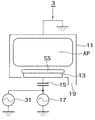
- the vacuum reaction chamber 11 is earthed as an anode.
- the substrate mounting stage 13 is electrically connected with the blocking capacitor 15 , and a processing target substrate S is disposed on an upper surface of the substrate mounting stage 13 .
- pusher pins 21 that lift up the processing target substrate S to be separated from the substrate mounting stage 13 are provided to the substrate mounting stage 13 , and they are electrically insulated from the substrate mounting stage 13 .
- the pusher pin 21 corresponds to, e.g., a temporary support member.
- One end of the high-frequency power supply 17 is earthed, and the other end of the same is connected with the blocking capacitor 15 .
- the processing target substrate S 3 is lifted up from a substrate mounting stage 13 by utilizing pusher pins 21 to generate a plasma using an oxygen (O 2 ) gas.
- O 2 oxygen
- the deposition DF on the inner wall of the vacuum reaction chamber 11 is removed, and dry etching processing is carried out with respect to the processing target substrate S 3 .
- the resist material 79 on the processing target substrate S 3 is removed, the coating type silicon oxide film 75 is exposed to the plasma, and this is used as a mask to proceed processing of the organic material film 73 as shown in FIG. 16 .
- the dry etching processing at this step corresponds to, e.g., second dry etching processing in this embodiment.
Landscapes
- Engineering & Computer Science (AREA)
- Physics & Mathematics (AREA)
- Plasma & Fusion (AREA)
- Chemical & Material Sciences (AREA)
- Analytical Chemistry (AREA)
- General Physics & Mathematics (AREA)
- Condensed Matter Physics & Semiconductors (AREA)
- Manufacturing & Machinery (AREA)
- Computer Hardware Design (AREA)
- Microelectronics & Electronic Packaging (AREA)
- Power Engineering (AREA)
- Drying Of Semiconductors (AREA)
- Internal Circuitry In Semiconductor Integrated Circuit Devices (AREA)
Abstract
Description
Claims (11)
Priority Applications (2)
| Application Number | Priority Date | Filing Date | Title |
|---|---|---|---|
| JP2007315749A JP5052313B2 (en) | 2007-10-29 | 2007-12-06 | Manufacturing method of semiconductor device |
| US12/926,135 US7943522B2 (en) | 2006-10-30 | 2010-10-27 | Manufacturing method of semiconductor device |
Applications Claiming Priority (2)
| Application Number | Priority Date | Filing Date | Title |
|---|---|---|---|
| JP2006294657A JP4755963B2 (en) | 2006-10-30 | 2006-10-30 | Manufacturing method of semiconductor device |
| JP2006-294657 | 2006-10-30 |
Related Child Applications (1)
| Application Number | Title | Priority Date | Filing Date |
|---|---|---|---|
| US12/926,135 Division US7943522B2 (en) | 2006-10-30 | 2010-10-27 | Manufacturing method of semiconductor device |
Publications (2)
| Publication Number | Publication Date |
|---|---|
| US20080138995A1 US20080138995A1 (en) | 2008-06-12 |
| US7846348B2 true US7846348B2 (en) | 2010-12-07 |
Family
ID=39445209
Family Applications (2)
| Application Number | Title | Priority Date | Filing Date |
|---|---|---|---|
| US11/927,080 Active 2029-06-13 US7846348B2 (en) | 2006-10-30 | 2007-10-29 | Manufacturing method of semiconductor device |
| US12/926,135 Expired - Fee Related US7943522B2 (en) | 2006-10-30 | 2010-10-27 | Manufacturing method of semiconductor device |
Family Applications After (1)
| Application Number | Title | Priority Date | Filing Date |
|---|---|---|---|
| US12/926,135 Expired - Fee Related US7943522B2 (en) | 2006-10-30 | 2010-10-27 | Manufacturing method of semiconductor device |
Country Status (2)
| Country | Link |
|---|---|
| US (2) | US7846348B2 (en) |
| JP (1) | JP4755963B2 (en) |
Families Citing this family (5)
| Publication number | Priority date | Publication date | Assignee | Title |
|---|---|---|---|---|
| JP5052313B2 (en) * | 2007-10-29 | 2012-10-17 | 株式会社東芝 | Manufacturing method of semiconductor device |
| JP4756063B2 (en) * | 2008-08-15 | 2011-08-24 | 株式会社東芝 | Manufacturing method of semiconductor device |
| JP6360770B2 (en) * | 2014-06-02 | 2018-07-18 | 東京エレクトロン株式会社 | Plasma processing method and plasma processing apparatus |
| US10784091B2 (en) | 2017-09-29 | 2020-09-22 | Taiwan Semiconductor Manufacturing Co., Ltd. | Process and related device for removing by-product on semiconductor processing chamber sidewalls |
| JP2022079159A (en) * | 2020-11-16 | 2022-05-26 | 東京エレクトロン株式会社 | Substrate processing method and substrate processing apparatus |
Citations (8)
| Publication number | Priority date | Publication date | Assignee | Title |
|---|---|---|---|---|
| US5756400A (en) | 1995-12-08 | 1998-05-26 | Applied Materials, Inc. | Method and apparatus for cleaning by-products from plasma chamber surfaces |
| US6136211A (en) * | 1997-11-12 | 2000-10-24 | Applied Materials, Inc. | Self-cleaning etch process |
| US20040097090A1 (en) * | 2002-08-26 | 2004-05-20 | Takanori Mimura | Silicon etching method |
| US20050022933A1 (en) * | 2003-08-01 | 2005-02-03 | Howard Bradley J. | Multi-frequency plasma reactor and method of etching |
| US20050241770A1 (en) | 2004-04-28 | 2005-11-03 | Tokyo Electron Limited | Substrate cleaning apparatus and method |
| US20060000552A1 (en) | 2004-07-05 | 2006-01-05 | Tokyo Electron Limited | Plasma processing apparatus and cleaning method thereof |
| JP2006019626A (en) | 2004-07-05 | 2006-01-19 | Tokyo Electron Ltd | Plasma treatment device and cleaning method thereof |
| US20060037703A1 (en) * | 2004-06-21 | 2006-02-23 | Tokyo Electron Limited | Plasma processing apparatus and method |
Family Cites Families (10)
| Publication number | Priority date | Publication date | Assignee | Title |
|---|---|---|---|---|
| JP3013446B2 (en) * | 1990-12-28 | 2000-02-28 | ソニー株式会社 | Dry etching method |
| JP3395490B2 (en) * | 1995-11-30 | 2003-04-14 | ソニー株式会社 | Resist ashing method and ashing apparatus used therefor |
| JP2000100791A (en) * | 1998-09-24 | 2000-04-07 | Sony Corp | Resist removal device |
| JP2001044178A (en) * | 1999-07-30 | 2001-02-16 | Matsushita Electronics Industry Corp | Board processing method and board processor |
| JP2002367967A (en) * | 2001-06-07 | 2002-12-20 | Matsushita Electric Ind Co Ltd | Method and apparatus for treating plasma |
| JP2004103872A (en) * | 2002-09-10 | 2004-04-02 | Hitachi Chem Co Ltd | Method of forming pattern in organic polymer film, method of forming multilayer wiring, and method of manufacturing semiconductor element |
| JP4024636B2 (en) * | 2002-09-20 | 2007-12-19 | 富士通株式会社 | Organic insulating film etching method and semiconductor device manufacturing method |
| JP4656364B2 (en) * | 2003-03-13 | 2011-03-23 | 東京エレクトロン株式会社 | Plasma processing method |
| JP2006245234A (en) * | 2005-03-02 | 2006-09-14 | Tokyo Electron Ltd | Plasma processing method and apparatus |
| US7432209B2 (en) * | 2006-03-22 | 2008-10-07 | Applied Materials, Inc. | Plasma dielectric etch process including in-situ backside polymer removal for low-dielectric constant material |
-
2006
- 2006-10-30 JP JP2006294657A patent/JP4755963B2/en not_active Expired - Fee Related
-
2007
- 2007-10-29 US US11/927,080 patent/US7846348B2/en active Active
-
2010
- 2010-10-27 US US12/926,135 patent/US7943522B2/en not_active Expired - Fee Related
Patent Citations (8)
| Publication number | Priority date | Publication date | Assignee | Title |
|---|---|---|---|---|
| US5756400A (en) | 1995-12-08 | 1998-05-26 | Applied Materials, Inc. | Method and apparatus for cleaning by-products from plasma chamber surfaces |
| US6136211A (en) * | 1997-11-12 | 2000-10-24 | Applied Materials, Inc. | Self-cleaning etch process |
| US20040097090A1 (en) * | 2002-08-26 | 2004-05-20 | Takanori Mimura | Silicon etching method |
| US20050022933A1 (en) * | 2003-08-01 | 2005-02-03 | Howard Bradley J. | Multi-frequency plasma reactor and method of etching |
| US20050241770A1 (en) | 2004-04-28 | 2005-11-03 | Tokyo Electron Limited | Substrate cleaning apparatus and method |
| US20060037703A1 (en) * | 2004-06-21 | 2006-02-23 | Tokyo Electron Limited | Plasma processing apparatus and method |
| US20060000552A1 (en) | 2004-07-05 | 2006-01-05 | Tokyo Electron Limited | Plasma processing apparatus and cleaning method thereof |
| JP2006019626A (en) | 2004-07-05 | 2006-01-19 | Tokyo Electron Ltd | Plasma treatment device and cleaning method thereof |
Also Published As
| Publication number | Publication date |
|---|---|
| JP4755963B2 (en) | 2011-08-24 |
| US20080138995A1 (en) | 2008-06-12 |
| US7943522B2 (en) | 2011-05-17 |
| JP2008112854A (en) | 2008-05-15 |
| US20110045615A1 (en) | 2011-02-24 |
Similar Documents
| Publication | Publication Date | Title |
|---|---|---|
| US5378311A (en) | Method of producing semiconductor device | |
| US7371690B2 (en) | Dry etching method and apparatus | |
| KR101772701B1 (en) | Plasma etching method, plasma etching apparatus and computer-readable storage medium | |
| KR100924853B1 (en) | Plasma etching method, plasma etching apparatus, control program and computer-readable storage medium | |
| US7943522B2 (en) | Manufacturing method of semiconductor device | |
| US8642482B2 (en) | Plasma etching method, control program and computer storage medium | |
| KR101295889B1 (en) | Method for manufacturing semiconductor device | |
| JP4351806B2 (en) | Improved technique for etching using a photoresist mask. | |
| TW201421581A (en) | Plasma etching method | |
| JP2019204815A (en) | Substrate processing method and substrate processing apparatus | |
| US20110171833A1 (en) | Dry etching method of high-k film | |
| US8664122B2 (en) | Method of fabricating a semiconductor device | |
| US20150194315A1 (en) | Plasma etching method | |
| EP0791669B1 (en) | Method for etching inside of cvd reaction chamber | |
| JP2001156041A (en) | Method for manufacturing semiconductor device and manufacturing apparatus for the same | |
| JP5052313B2 (en) | Manufacturing method of semiconductor device | |
| JPWO2016079818A1 (en) | Plasma processing method | |
| US11417527B2 (en) | Method and device for controlling a thickness of a protective film on a substrate | |
| US11658040B2 (en) | Plasma processing method | |
| JP5815459B2 (en) | Plasma etching method | |
| US6403489B1 (en) | Method for removing polymer stacked on a lower electrode within an etching reaction chamber | |
| KR20220082979A (en) | Substrate processing method of substrate processing apparatus | |
| KR20230147596A (en) | Plasma treatment method | |
| JP2007251034A (en) | Plasma processing method | |
| JPH0878515A (en) | Fabrication of semiconductor device |
Legal Events
| Date | Code | Title | Description |
|---|---|---|---|
| AS | Assignment |
Owner name: KABUSHIKI KAISHA TOSHIBA, JAPAN Free format text: ASSIGNMENT OF ASSIGNORS INTEREST;ASSIGNOR:OMURA, MITSUHIRO;REEL/FRAME:020475/0876 Effective date: 20071128 |
|
| STCF | Information on status: patent grant |
Free format text: PATENTED CASE |
|
| FEPP | Fee payment procedure |
Free format text: PAYOR NUMBER ASSIGNED (ORIGINAL EVENT CODE: ASPN); ENTITY STATUS OF PATENT OWNER: LARGE ENTITY |
|
| FPAY | Fee payment |
Year of fee payment: 4 |
|
| AS | Assignment |
Owner name: TOSHIBA MEMORY CORPORATION, JAPAN Free format text: ASSIGNMENT OF ASSIGNORS INTEREST;ASSIGNOR:KABUSHIKI KAISHA TOSHIBA;REEL/FRAME:043709/0035 Effective date: 20170706 |
|
| MAFP | Maintenance fee payment |
Free format text: PAYMENT OF MAINTENANCE FEE, 8TH YEAR, LARGE ENTITY (ORIGINAL EVENT CODE: M1552) Year of fee payment: 8 |
|
| AS | Assignment |
Owner name: K.K. PANGEA, JAPAN Free format text: MERGER;ASSIGNOR:TOSHIBA MEMORY CORPORATION;REEL/FRAME:055659/0471 Effective date: 20180801 Owner name: KIOXIA CORPORATION, JAPAN Free format text: CHANGE OF NAME AND ADDRESS;ASSIGNOR:TOSHIBA MEMORY CORPORATION;REEL/FRAME:055669/0001 Effective date: 20191001 Owner name: TOSHIBA MEMORY CORPORATION, JAPAN Free format text: CHANGE OF NAME AND ADDRESS;ASSIGNOR:K.K. PANGEA;REEL/FRAME:055669/0401 Effective date: 20180801 |
|
| MAFP | Maintenance fee payment |
Free format text: PAYMENT OF MAINTENANCE FEE, 12TH YEAR, LARGE ENTITY (ORIGINAL EVENT CODE: M1553); ENTITY STATUS OF PATENT OWNER: LARGE ENTITY Year of fee payment: 12 |