US7809349B1 - Radio frequency filter using intermediate frequency impedance translation - Google Patents
Radio frequency filter using intermediate frequency impedance translation Download PDFInfo
- Publication number
- US7809349B1 US7809349B1 US11/739,725 US73972507A US7809349B1 US 7809349 B1 US7809349 B1 US 7809349B1 US 73972507 A US73972507 A US 73972507A US 7809349 B1 US7809349 B1 US 7809349B1
- Authority
- US
- United States
- Prior art keywords
- impedance
- filter
- frequency
- input
- local oscillator
- Prior art date
- Legal status (The legal status is an assumption and is not a legal conclusion. Google has not performed a legal analysis and makes no representation as to the accuracy of the status listed.)
- Active, expires
Links
Images


Classifications
-
- H—ELECTRICITY
- H04—ELECTRIC COMMUNICATION TECHNIQUE
- H04B—TRANSMISSION
- H04B1/00—Details of transmission systems, not covered by a single one of groups H04B3/00 - H04B13/00; Details of transmission systems not characterised by the medium used for transmission
- H04B1/06—Receivers
- H04B1/16—Circuits
- H04B1/26—Circuits for superheterodyne receivers
- H04B1/28—Circuits for superheterodyne receivers the receiver comprising at least one semiconductor device having three or more electrodes
Definitions
- the present invention relates to radio frequency (RF) filters, which are used in RF communications systems.
- RF radio frequency
- RF filters are commonly used in RF communications circuits to remove signals at unwanted RF frequencies.
- An RF receiver may use RF filters to remove unwanted signals that have been received through an antenna, or signals from other circuitry, such as an RF transmitter.
- An RF transmitter may use RF filters to remove noise from a transmitted signal.
- a common type of filter circuit is a surface acoustic wave (SAW) filter, which may be used as a bandpass filter.
- SAW surface acoustic wave
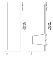
- FIG. 1 A filter input F IN feeds the bandpass filter 10 , which filters out high frequency signals and low frequency signals.
- a filter output F OUT is provided from the bandpass filter 10 .
- FIG. 2A is a graph showing a constant amplitude signal at all frequencies being applied to the filter input F IN .
- FIG. 2B shows the response of the bandpass filter 10 at the filter output F OUT .
- Frequencies below a high pass filter break frequency F HP are filtered out.
- Frequencies above a low pass filter break frequency F LP are filtered out.
- Frequencies between the two break frequencies F HP , F LP are allowed to pass through the bandpass filter 10 .
- a center frequency F C is the average of the high pass filter break frequency F HP and the low pass filter break frequency F LP .
- RF bandpass filters are typically limited in their roll-off characteristics. It is difficult to produce an RF bandpass filter with a high enough Q to adequately filter out all of the unwanted signals and noise. Q indicates the effectiveness of an RF filter. This is one of the reasons that super-heterodyne receivers are used.
- a received RF signal is mixed with an RF local oscillator signal to create an intermediate frequency (IF) signal, the frequency of which is a difference between the frequency of the received RF signal and the frequency of an RF local oscillator signal. Since the IF signal is at a lower frequency, any interfering signals may be filtered out more effectively in the IF section of the receiver than in the RF section.
- IF intermediate frequency
- the frequency of the RF local oscillator signal is the center frequency of a desired received RF signal
- RF bandpass filters may have to be tuned to the desired received center frequency and must be stable in the presence of environmental changes, such as temperature.
- an RF filter having the high Q roll-off characteristics of an IF filter which is aligned with the desired received center frequency resulting in improved filtering characteristics.
- the present invention is an RF filter that translates impedances of an IF circuit to create a filter with an RF center frequency having the high Q roll-off characteristics of an IF filter.
- the RF filter is self-aligned with the frequency of an RF local oscillator.
- the RF filter has an impedance divider, which is formed by coupling an RF impedance circuit to a translated IF impedance circuit.
- the translated IF impedance circuit includes an RF passive mixer and an IF impedance circuit.
- the mixer translates the impedance of the IF impedance circuit by mixing an RF input signal with an RF local oscillator signal, which determines the RF center frequency. Filtered RF signals may be provided by the impedance divider.
- filtered IF signals may be provided by the IF impedance circuit.
- the IF impedance circuit presents a high impedance at harmonics of the RF local oscillator signal.
- RF filters can be created using this technique, including but not limited to RF bandpass filters, RF notch filters, and RF double notch filters. Such filters could be used in RF transmitters, RF receivers, or both.
- the RF impedance circuit may be series coupled in an RF signal path, and the translated IF impedance circuit may be coupled to ground.
- the RF passive mixer and the IF impedance circuit may be quadrature to eliminate image load impedances creating image responses as a result of mixing.
- RF signals, IF signals, or both may include differential signals.
- the RF passive mixer may be a switching RF passive mixer, which uses the RF local oscillator signal to enable and disable switching elements between an RF input and an IF output.
- the RF impedance circuit may be provided by an output impedance of an RF amplifier that feeds the translated IF impedance circuit.
- An RF receiver may use the present invention to remove unwanted signals that have been received through an antenna, or signals from other circuitry, such as an RF transmitter.
- An RF receiver may use filtered IF signals from the IF impedance circuit.
- the filtered IF signals may be at any IF frequency, including but not limited to very low IF (VLIF) and direct current (DC) resulting from direct conversion.
- An RF transmitter may use the present invention to remove noise from a transmitted signal.
- FIG. 1 shows a bandpass filter according to the prior art.
- FIGS. 2A and 2B are graphs showing the frequency response of a SAW filter used as the bandpass filter of FIG. 1 .
- FIG. 3A shows one embodiment of the present invention, which is a series coupled RF filter using IF impedance translation.
- FIG. 3B shows an alternate embodiment of the present invention, which is a parallel coupled RF filter using IF impedance translation.
- FIG. 4 shows the RF filter of FIG. 3A wherein the RF signal path is quadrature.
- FIG. 5 shows the RF filter of FIG. 4 wherein the local oscillator signals are not quadrature.
- FIG. 6 shows the RF filter of FIG. 3A wherein there is no RF filter output; however, filtered IF outputs are taken from the IF impedance circuit.
- FIG. 7 adds differential signals to the RF filter of FIG. 6 .
- FIG. 8 shows a series RF impedance circuit being provided by an RF amplifier.
- FIG. 9 adds series inductors and capacitors to the IF impedance circuit of FIG. 7 .
- FIG. 10 shows details of the RF passive mixer of FIG. 7 .
- FIG. 11A is a graph showing the IF impedance of the IF impedance circuit when the present invention is used as an RF bandpass filter.
- FIG. 11B is a graph showing the RF impedance, which is the translated IF impedance of the IF impedance circuit of FIG. 11A .
- FIG. 12A is a graph showing the IF impedance of the IF impedance circuit when the present invention is used as an RF notch filter.
- FIG. 12B is a graph showing the RF impedance, which is the translated IF impedance of the IF impedance circuit of FIG. 12A .
- FIG. 13A is a graph showing the IF impedance of the IF impedance circuit when the present invention is used as an RF double notch filter.
- FIG. 13B is a graph showing the RF impedance, which is the translated IF impedance of the IF impedance circuit of FIG. 13A .
- FIG. 14 shows the present invention used in a full duplex transceiver circuit.
- FIG. 15 adds an RF double notch filter to the full duplex transceiver circuit of FIG. 14 .
- FIG. 16 shows the present invention used as a pre-low noise amplifier (LNA) bandpass filter in a half duplex transceiver circuit.
- LNA pre-low noise amplifier
- FIG. 17 adds an RF notch filter to the RF transmitter of FIG. 14 .
- FIG. 18 adds the RF notch filter to the RF receiver of FIG. 14 .
- the present invention is an RF filter that translates impedances of an IF circuit to create a filter with an RF center frequency having the high Q roll-off characteristics of an IF filter.
- the RF filter is self-aligned with the frequency of an RF local oscillator.
- the RF filter has an impedance divider, which is formed by coupling an RF impedance circuit to a translated IF impedance circuit.
- the translated IF impedance circuit includes an RF passive mixer and an IF impedance circuit.
- the mixer translates the impedance of the IF impedance circuit by mixing an RF input signal with an RF local oscillator signal, which determines the RF center frequency. Both the magnitude and the frequency of the impedance may be translated.
- the magnitude of the impedance translation is dependent on the duty-cycle of the RF local oscillator.
- Filtered RF signals may be provided by the impedance divider; however, input impedances from downstream circuitry, such as an amplifier stage, will become part of the impedance divider and may influence RF filter behavior.
- Filtered IF signals may be provided by the IF impedance circuit.
- the IF impedance circuit presents a high impedance at harmonics of the RF local oscillator signal.
- the high impedance is typically greater than the impedance of the RF impedance circuit.
- the RF passive mixer may translate IF impedances into RF impedances at the frequency of the RF local oscillator signal, and at harmonics of the RF local oscillator signal; therefore, the IF impedance circuit presents high impedances at harmonics of the RF local oscillator signal; however, any impedances at harmonics of the RF local oscillator signal may affect the magnitude of translated impedances.
- Certain embodiments of the present invention may include series coupled inductive elements in the IF impedance circuit to provide the high impedances. Values of the inductive elements may be chosen to resonate with parasitic capacitances at harmonics of the RF local oscillator signal to maximize the high impedances at these specific frequencies.
- RF filters can be created using this technique, including but not limited to RF bandpass filters, RF notch filters, and RF double notch filters. Such filters could be used in RF transmitters, RF receivers, or both.
- the RF mixer is spared large amplitudes of interfering signals, which can significantly improve intermodulation performance, relax compression point requirements in the IF section, or both.
- the RF impedance circuit may be series coupled in an RF signal path, and the translated IF impedance circuit may be coupled to ground.
- some embodiments of the present invention may couple the RF impedance circuit in parallel with the translated IF impedance circuit, which are then both driven from a current source. Filtered RF signals may be provided by the parallel coupling of the RF impedance circuit and the translated IF impedance circuit. Filtered IF signals may be provided by the IF impedance circuit.
- the RF passive mixer and the IF impedance circuit may be quadrature to eliminate image load impedances creating image responses as a result of mixing. Any unused quadrature inputs may be grounded to ensure proper mixing and IF impedance translation behavior.
- RF signals, IF signals, or both may include differential signals.
- the RF passive mixer may be of any architecture that translates an IF impedance presented to an IF output of the RF passive mixer to an RF input impedance at an RF input of the RF passive mixer.
- the RF passive mixer may be a switching RF passive mixer, which uses the RF local oscillator signal to enable and disable switching elements between an RF input and an IF output.
- the RF impedance circuit may be provided by an output impedance of an RF amplifier that feeds the translated IF impedance circuit.
- An RF receiver may use the present invention to remove unwanted signals that have been received through an antenna, or signals from other circuitry, such as an RF transmitter.
- An RF receiver may use filtered IF signals from the IF impedance circuit.
- the filtered IF signals may be at any IF frequency, including but not limited to very low IF (VLIF) and direct current (DC) resulting from direct conversion.
- VLIF very low IF
- DC direct current
- An RF transmitter may use the present invention to remove noise from a transmitted signal.
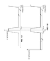
- FIG. 3A shows one embodiment of the present invention, which is an RF filter 12 using IF impedance translation.
- a series RF impedance circuit 14 receives input signals into an RF filter input RF FIN .
- the series RF impedance circuit 14 is coupled to a translated IF impedance circuit 16 to form an RF impedance divider, which provides RF filtering behavior, and may provide an RF filter output RF FOUT .
- the translated IF impedance circuit 16 includes an RF passive mixer 18 , which feeds an IF impedance circuit 20 .
- the RF passive mixer 18 receives quadrature local oscillator signals into an in-phase local oscillator input LO I and a quadrature-phase local oscillator input LO Q .
- the RF passive mixer 18 mixes the quadrature local oscillator signals with an RF input signal from the series RF impedance circuit 14 to create IF output signals provided to an in-phase IF output IF OUTI and a quadrature-phase IF output IF OUTQ .
- the IF outputs IF OUTI , IF OUTQ are coupled to the IF impedance circuit 20 , which presents IF impedances to the IF outputs IF OUTI , IF OUTQ for translation into RF impedances.
- the response of the IF impedances to different frequencies determines the behavior of the RF filter 12 .
- the mixing by the RF passive mixer 18 translates the impedances of the IF impedance circuit 20 into an RF impedance.
- the translation process creates a mirror of the IF impedances about an RF center frequency, which is equal to the frequency of the RF local oscillator signals.
- signals at quadrature-phase inputs and outputs are phase-shifted approximately 90 degrees from signals at in-phase inputs and outputs.
- FIG. 3B shows an alternate embodiment of the present invention.
- the RF impedance circuit 14 receives input signals into an RF filter input RF FIN .
- the RF impedance circuit 14 is coupled in parallel with the translated IF impedance circuit 16 .
- Upstream circuitry provides input signals into the RF filter input RF FIN .
- the upstream circuitry has a high output impedance; therefore, the RF filtering behavior is provided from the RF impedance circuit 14 that is coupled in parallel with the translated IF impedance circuit 16 .
- An RF filter output RF FOUT may be provided by coupling to the RF filter input RF FIN .
- FIG. 4 differs from the RF filter 12 of FIG. 3A in that the RF signal path in FIG. 4 is quadrature.
- An in-phase RF input signal is received into an in-phase RF filter input RF FINI of the series RF impedance circuit 14 .
- a quadrature-phase RF input signal is received into a quadrature-phase RF filter input RF FINQ of the series RF impedance circuit 14 .
- the series RF impedance circuit 14 is coupled to the translated IF impedance circuit 16 to form the RF impedance divider, which provides RF filtering behavior, and may provide an in-phase RF filter output RF FOUTI and a quadrature-phase RF filter output RF FOUTQ .
- FIG. 5 differs from the RF filter 12 of FIG. 4 in that the local oscillator signals in FIG. 5 are not quadrature.
- the RF passive mixer 18 receives a quadrature local oscillator signal into a single local oscillator input LO.
- FIG. 6 differs from the RF filter 12 of FIG. 3A in that the RF filter output of FIG. 3A is taken from the output of the series RF impedance circuit 14 , whereas in FIG. 6 there is no RF filter output; however, the IF impedance circuit 20 provides an in-phase filtered IF output IF FOUTI and a quadrature-phase filtered IF output IF FOUTQ to provide IF signals for processing by downstream receiver circuitry.
- FIG. 7 adds differential signals to the RF filter 12 of FIG. 6 .
- the series RF impedance circuit 14 receives differential input signals into a first differential RF filter input RF FIN1 and a second differential RF filter input RF FIN2 .
- the series RF impedance circuit 14 is coupled to the translated IF impedance circuit 16 to form the RF impedance divider, which provides RF filtering behavior, and provides differential RF filter output signals to the translated IF impedance circuit 16 on a first differential RF filter output RF FOUT1 and a second differential RF filter output RF FOUT2 .
- the RF passive mixer 18 receives differential quadrature local oscillator signals into a first differential in-phase local oscillator input LO I1 , a second differential in-phase local oscillator input LO I2 , a first differential quadrature-phase local oscillator input LO Q1 , and a second differential quadrature-phase local oscillator input LO Q2 .
- the RF passive mixer 18 mixes the differential quadrature local oscillator signals with the differential RF filter output signals to create differential IF output signals provided to a first differential in-phase IF output IF OUTI1 , a second differential in-phase IF output IF OUTI2 , a first differential quadrature-phase IF output IF OUTQ1 , and a second differential quadrature-phase IF output IF OUTQ2 .
- the differential IF outputs IF OUTI1 , IF OUTI2 , IF OUTQ1 , IF OUTQ2 are coupled to the IF impedance circuit 20 , which presents differential IF impedances to the differential IF outputs IF OUTI1 , IF OUTI2 , IF OUTQ1 , IF OUTQ2 for translation into RF impedances.
- the IF impedance circuit 20 provides a first differential in-phase filtered IF output IF FOUTI1 , a second differential in-phase filtered IF output IF FOUTI2 , a first differential quadrature-phase filtered IF output IF FOUTQ1 , and a second differential quadrature-phase filtered IF output IF FOUTQ2 to provide differential filtered IF signals for processing by downstream receiver circuitry.
- first differential inputs and outputs are phase-shifted from second differential inputs and outputs by approximately 180 degrees.
- FIG. 8 shows the series RF impedance circuit 14 being provided by a differential RF amplifier 22 .
- the differential RF amplifier 22 receives differential input signals into a first differential input RF IN1 and a second differential input RF IN2 .
- the differential RF amplifier 22 can be represented as having an ideal non-inverting amplifier 24 feeding a non-inverting output impedance R 2 , and an ideal inverting amplifier 26 feeding an inverting output impedance R 3 .
- the differential output impedances R 2 , R 3 form the series RF impedance circuit 14 .
- FIG. 9 adds series inductors and capacitors to the IF impedance circuit 20 of FIG. 7 .
- the series inductors provide high pass filtering to present high impedances at harmonics of the RF local oscillator signal.
- the series capacitors provide low pass filtering to present high impedances at low IF frequencies.
- the low pass filtering is translated into bandpass filtering by the RF passive mixer 18 .
- a first inductor L 1 is coupled to the first differential in-phase IF output IF OUTI1 .
- a first capacitor C 1 and the input to a first buffer U 1 are coupled to the first inductor L 1 .
- the first differential in-phase IF output IF FOUTI1 is provided from the output of the first buffer U 1 .
- a second inductor L 2 is coupled to the second differential in-phase IF output IF OUTI2 .
- a second capacitor C 2 and the input to a second buffer U 2 are coupled to the second inductor L 2 .
- the second differential in-phase IF output IF FOUTI2 is provided from the output of the second buffer U 2 .
- a third inductor L 3 is coupled to the first differential quadrature-phase IF output IF OUTQ1 .
- a third capacitor C 3 and the input to a third buffer U 3 are coupled to the third inductor L 3 .
- the first differential quadrature-phase IF output IF FOUTQ1 is provided from the output of the third buffer U 3 .
- a fourth inductor L 4 is coupled to the second differential quadrature-phase IF output IF OUTQ2 .
- a fourth capacitor C 4 and the input to a fourth buffer U 4 are coupled to the fourth inductor L 4 .
- the second differential quadrature-phase IF output IF FOUTQ2 is provided from the output of the fourth buffer U 4 .
- Inductance values of the inductors L 1 , L 2 , L 3 , L 4 may be chosen to resonate with any parasitic capacitances on the IF outputs IF OUTI1 , IF OUTI2 , IF OUTQ1 , IF OUTQ2 of the RF passive mixer 18 .
- capacitors may be added to the IF outputs IF OUTI1 , IF OUTI2 , IF OUTQ1 , IF OUTQ2 to resonate with the inductors L 1 , L 2 , L 3 , L 4 , which provides a more deterministic resonant frequency than just relying on parasitic capacitance and enables the use of smaller inductors to save space and cost. Additionally, the values of the capacitors can be changed to match local oscillator frequency changes.
- the resonant frequency may be around twice to three times the frequency of the local oscillator signals.
- a high impedance load is thus presented at the IF port at the second and other significant harmonics of the local oscillator signals; therefore, the component of the impedance observed at the RF port of the mixers due to the translated IF port impedances will be high.
- the net impedance observed at the RF port will be the parallel equivalent of this high impedance with any other IF impedance translated in frequency by the RF passive mixer 18 .
- the net impedance observed at the RF port can be made to follow the impedance at the IF port but scaled in magnitude and shifted in frequency by a factor of the frequency of the local oscillator signals.
- the magnitude scaling is a function of the duty cycle of the local oscillator signals and the magnitude of impedances at harmonics of the RF local oscillator signal. If the value of the inductors L 1 , L 2 , L 3 , L 4 are not closely matched, then IF image impedances may be presented at harmonics of the RF local oscillator signal. In other embodiments of the present invention, the capacitors C 1 , C 2 , C 3 , C 4 , the buffers U 1 , U 2 , U 3 , U 4 , or both may be omitted.
- FIG. 10 shows details of the RF passive mixer 18 of FIG. 7 , which is a differential switching RF passive mixer using field effect transistors (FETs) as switching elements.
- the first differential RF filter output RF FOUT1 is coupled to the drains of a first in-phase transistor 28 , a second in-phase transistor 30 , a first quadrature-phase transistor 32 , and a second quadrature-phase transistor 34 .
- the second differential RF filter output RF FOUT2 is coupled to the drains of a third in-phase transistor 36 , a fourth in-phase transistor 38 , a third quadrature-phase transistor 40 , and a fourth quadrature-phase transistor 42 .
- the first differential in-phase local oscillator input LO I1 is coupled to the gates of the first in-phase transistor 28 and the fourth in-phase transistor 38 .
- the second differential in-phase local oscillator input LO I2 is coupled to the gates of the third in-phase transistor 36 and the second in-phase transistor 30 .
- the first differential quadrature-phase local oscillator input LO Q1 is coupled to the gates of the first quadrature-phase transistor 32 and the fourth quadrature-phase transistor 42 .
- the second differential quadrature-phase local oscillator input LO Q2 is coupled to the gates of the third quadrature-phase transistor 40 and the second quadrature-phase transistor 34 .
- the first differential in-phase IF output IF OUTI1 is coupled to the sources of the fourth in-phase transistor 38 and the second in-phase transistor 30 .
- the second differential in-phase IF output IF OUTI2 is coupled to the sources of the first in-phase transistor 28 and the third in-phase transistor 36 .
- the first differential quadrature-phase IF output IF OUTQ1 is coupled to the sources of the fourth quadrature-phase transistor 42 and the second quadrature-phase transistor 34 .
- the second differential quadrature-phase IF output IF OUTQ2 is coupled to the sources of the first quadrature-phase transistor 32 and the third quadrature-phase transistor 40 .
- FIG. 11A is a graph showing the IF impedance of the IF impedance circuit 20 when the present invention is used as an RF bandpass filter.
- the IF impedance is a low pass filter, which passes frequencies from DC to an IF low pass break frequency F IFLP , and blocks frequencies from the IF low pass break frequency F IFLP to an IF harmonic blocking break frequency F IFHM . Frequencies above the IF harmonic blocking break frequency F IFHM are passed to present high impedances at harmonics of the RF local oscillator signals.
- FIG. 11B is a graph showing the RF impedance, which is the translated IF impedance of the IF impedance circuit 20 of FIG. 11A .
- a mirror image of the IF impedance is created that is centered about the frequency of the RF local oscillator signals F LO .
- the shape of the RF impedance response graph is very similar to the shape of the IF impedance response graph. Finite switch resistances, resonances, and loading at the RF inputs to the RF passive mixer and the effects of IF port impedances at harmonics of the local oscillator signals may affect the shape of the RF impedance response graph.
- An RF low pass break frequency F RFLP is located at F LO +F IFLP .
- An RF high pass break frequency F RFHP is located at F LO ⁇ F IFLP .
- An RF harmonic blocking break frequency F RFHM is located at F LO +F IFHM . Frequencies above the RF harmonic blocking break frequency F RFHM are passed to present high impedances at harmonics of the RF local oscillator signals.
- the low pass side of the filter and the high pass side of the filter combine to form the bandpass filter.
- the bandwidth of the bandpass filter is equal to approximately 2*F IFLP .
- FIG. 12A is a graph showing the IF impedance of the IF impedance circuit 20 when the present invention is used as an RF notch filter.
- the IF impedance is a high pass filter, which blocks frequencies from DC to an IF high pass break frequency F IFHP , and passes frequencies above the IF high pass break frequency F IFHP .
- FIG. 12B is a graph showing the RF impedance, which is the translated IF impedance of the IF impedance circuit 20 of FIG. 12A .
- the shape of the RF impedance response graph is identical to the shape of the IF impedance response graph.
- An RF low notch break frequency F RFNL is located at F LO ⁇ F IFHP .
- An RF high notch break frequency F RFNH is located at F LO +F IFHP .
- the low notch side of the filter and the high notch side of the filter combine to form the notch filter.
- the bandwidth of the notch filter is equal to approximately 2*F IFHP .
- FIG. 13A is a graph showing the IF impedance of the IF impedance circuit 20 when the present invention is used as an RF double notch filter.
- the IF impedance is a notch filter, which blocks at an IF notch frequency F IFN , which may be determined by a series resonant circuit.
- the bandwidth of the notch filter may be determined by the Q of the series resonant circuit.
- FIG. 13B is a graph showing the RF impedance, which is the translated IF impedance of the IF impedance circuit 20 of FIG. 13A .
- a mirror image of the IF impedance is created that is centered about the frequency of the RF local oscillator signals F LO .
- the shape of the RF impedance response graph is identical to the shape of the IF impedance response graph.
- An RF low double notch frequency F RFDNL is located at F LO ⁇ F IFN .
- An RF high double notch frequency F RFDNH is located at F LO +F IFN .
- FIG. 14 shows the present invention used in a full duplex transceiver circuit 44 , which includes an RF transmitter 46 and an RF receiver 48 .
- the RF transmitter and receiver 46 , 48 are coupled to an RF antenna 50 through an RF duplexer 52 .
- the RF transmitter 46 includes an RF modulator 54 , which feeds an RF driver stage 56 .
- the RF driver stage 56 feeds an RF final stage 58 , which feeds the RF duplexer 52 .
- a transmitter frequency synthesizer 60 provides a transmitter in-phase local oscillator signal LO TI and a transmitter quadrature-phase local oscillator signal LO TQ to the RF modulator 54 and a bandpass shunt impedance circuit 62 .
- the bandpass shunt impedance circuit 62 includes a version of the translated IF impedance circuit 16 that provides bandpass functionality.
- the bandpass shunt impedance circuit 62 and the output impedance of the RF driver stage 56 form a transmitter RF bandpass filter, which is used to reduce transmitter noise outside the passband of the transmitter RF bandpass filter. Since the center frequency of the transmitter RF bandpass filter is self-aligned to the transmitter local oscillator signals LO TI , LO TQ , the transmitter RF bandpass filter may be tuned to pass signals from different frequency bands.
- the local oscillator signals to the bandpass shunt impedance circuit 62 may be provided from a source other than the transmitter frequency synthesizer 60 .
- the RF receiver 48 includes a first receiver RF bandpass filter 64 , which receives RF signals from the RF duplexer 52 .
- the RF receiver 48 feeds an LNA 66 , which feeds an RF bandpass filter and down converter 68 .
- a receiver frequency synthesizer 70 provides a receiver in-phase local oscillator signal LO RI and a transmitter quadrature-phase local oscillator signal LO RQ to the RF bandpass filter and down converter 68 , which includes the RF passive mixer 18 and a version of the translated IF impedance circuit 16 that provides bandpass functionality and provides the filtered IF outputs IF FOUTI , IF FOUTQ .
- the RF bandpass filter and down converter 68 and the output impedance of the LNA 66 form a second receiver RF bandpass filter, which is used to reject received interfering signals and RF transmitter signals outside the passband of the second receiver RF bandpass filter.
- FIG. 15 adds an RF double notch impedance circuit 72 to the full duplex transceiver circuit 44 of FIG. 14 .
- the LNA 66 feeds the RF double notch impedance circuit 72 , which includes a version of the translated IF impedance circuit 16 that provides double notch filter functionality.
- the receiver frequency synthesizer 70 provides the receiver local oscillator signals LO RI , LO RQ to the RF double notch impedance circuit 72 .
- the RF double notch impedance circuit 72 and the output impedance of the LNA 66 form an RF double notch filter.
- the RF double notch filter is used to reject RF transmitter signals from the RF duplexer 52 or other sources. Since the center frequency of the RF double notch filter is self-aligned to the receiver local oscillator signals LO RI , LO RQ , the RF double notch filter may be tuned to receive signals from different frequency bands. In a different embodiment of the present invention, the local oscillator signals to the RF double notch impedance circuit 72 may be provided from a source other than the receiver frequency synthesizer 70 .
- FIG. 16 shows the present invention used as a pre-LNA bandpass filter in a half duplex transceiver circuit 74 .
- the RF transmitter and receiver 46 , 48 are coupled to the RF antenna 50 through an RF switch 73 .
- the bandpass shunt impedance circuit 62 and the output impedance of the RF antenna 50 form a pre-LNA RF bandpass filter, which is used to remove received signals and noise outside the passband of the pre-LNA RF bandpass filter.
- the receiver frequency synthesizer 70 provides the receiver local oscillator signals LO RI , LO RQ to the bandpass shunt impedance circuit 62 .
- the pre-LNA RF bandpass filter may be tuned to receive signals from different frequency bands.
- the local oscillator signals to the bandpass shunt impedance circuit 62 may be provided from a source other than the receiver frequency synthesizer 70 .
- the pre-LNA RF bandpass filter may be used in a receive only system that does not have the RF transmitter 46 and the RF switch 73 . In such a system, the RF receiver 48 is coupled directly to the RF antenna 50 .
- FIG. 17 replaces the bandpass shunt impedance circuit 62 of FIG. 14 with an RF notch impedance circuit 75 .
- the RF driver stage 56 feeds the RF notch impedance circuit 75 , which includes a version of the translated IF impedance circuit 16 that provides notch filter functionality.
- the receiver frequency synthesizer 70 provides the receiver local oscillator signals LO RI , LO RQ to the RF notch impedance circuit 75 .
- the RF notch impedance circuit 75 and the output impedance of the RF driver stage 56 form a transmitter RF notch filter.
- the notch of the transmitter RF notch filter is at the receiver frequency; therefore, the transmitter RF notch filter is used to remove RF transmitter signals that may interfere with the RF receiver 48 . Since the center frequency of the transmitter RF notch filter is self-aligned to the receiver local oscillator signals LO RI , LO RQ , the transmitter RF notch filter may be tuned to remove noise signals from different receiver frequency bands. In a different embodiment of the present invention, the local oscillator signals to the RF notch impedance circuit 75 may be provided from a source other than the receiver frequency synthesizer 70 .
- FIG. 18 adds the RF notch impedance circuit 75 to the RF receiver 48 of FIG. 14 .
- the LNA 66 feeds the RF notch impedance circuit 75 .
- the transmitter frequency synthesizer 60 provides the transmitter local oscillator signals LO TI , LO TQ to the RF notch impedance circuit 75 .
- the RF notch impedance circuit 75 and the output impedance of the LNA 66 form a receiver RF notch filter.
- the notch of the receiver RF notch filter is at the transmitter frequency; therefore, the receiver RF notch filter is used to remove RF transmitter signals that may interfere with the RF receiver 48 .
- the receiver RF notch filter may be tuned to remove noise signals from different transmitter frequency bands.
- the local oscillator signals to the RF notch impedance circuit 75 may be provided from a source other than the transmitter frequency synthesizer 60 .
Abstract
Description
Claims (20)
Priority Applications (1)
| Application Number | Priority Date | Filing Date | Title |
|---|---|---|---|
| US11/739,725 US7809349B1 (en) | 2006-10-18 | 2007-04-25 | Radio frequency filter using intermediate frequency impedance translation |
Applications Claiming Priority (2)
| Application Number | Priority Date | Filing Date | Title |
|---|---|---|---|
| US82999406P | 2006-10-18 | 2006-10-18 | |
| US11/739,725 US7809349B1 (en) | 2006-10-18 | 2007-04-25 | Radio frequency filter using intermediate frequency impedance translation |
Publications (1)
| Publication Number | Publication Date |
|---|---|
| US7809349B1 true US7809349B1 (en) | 2010-10-05 |
Family
ID=42797815
Family Applications (1)
| Application Number | Title | Priority Date | Filing Date |
|---|---|---|---|
| US11/739,725 Active 2029-04-18 US7809349B1 (en) | 2006-10-18 | 2007-04-25 | Radio frequency filter using intermediate frequency impedance translation |
Country Status (1)
| Country | Link |
|---|---|
| US (1) | US7809349B1 (en) |
Cited By (35)
| Publication number | Priority date | Publication date | Assignee | Title |
|---|---|---|---|---|
| US20100267354A1 (en) * | 2009-04-17 | 2010-10-21 | Broadcom Corporation | Frequency Translated Filter |
| US20100317308A1 (en) * | 2009-06-16 | 2010-12-16 | Broadcom Corporation | Area Reduction Techniques for Saw-Less Receivers |
| US20100317311A1 (en) * | 2009-06-10 | 2010-12-16 | Broadcom Corporation | Protection for SAW-Less Receivers |
| US20110003569A1 (en) * | 2009-07-02 | 2011-01-06 | Broadcom Corporation | Frequency Translated Filters For Wideband Applications |
| US20110003572A1 (en) * | 2009-07-02 | 2011-01-06 | Broadcom Corporation | Layout Techniques For Frequency Translated Filters |
| US20110028115A1 (en) * | 2009-07-30 | 2011-02-03 | Broadcom Corporation | Receiver apparatus having filters implemented using frequency translation techniques |
| US8644785B2 (en) * | 2009-04-07 | 2014-02-04 | Intel Mobile Communications GmbH | Filtering using impedance translator |
| US20150092625A1 (en) * | 2013-03-15 | 2015-04-02 | Rf Micro Devices, Inc. | Hybrid active and passive tunable rf filters |
| US9071300B2 (en) * | 2012-07-23 | 2015-06-30 | Wistron Neweb Corporation | Signal transceiver with enhanced return loss in power-off state |
| US9391717B2 (en) | 2012-11-13 | 2016-07-12 | Stephane Laurent-Michel | Method and system for signal dynamic range improvement for frequency-division duplex communication systems |
| US9543995B1 (en) * | 2013-02-05 | 2017-01-10 | Marvell International Ltd. | Analog front end receivers with resonant mixer configured to reject local oscillator harmonics |
| US9584077B2 (en) * | 2015-05-22 | 2017-02-28 | Signalchip Innovations Private Limited | Impedance synthesis for optimum frequency response of a radio frequency (RF) amplifier |
| US9628045B2 (en) | 2013-08-01 | 2017-04-18 | Qorvo Us, Inc. | Cooperative tunable RF filters |
| US9680521B2 (en) | 2012-07-09 | 2017-06-13 | Telefonaktiebolaget Lm Ericsson (Publ) | Transceiver front-end for blocking transmit or receive frequency signals |
| US9705542B2 (en) | 2013-06-06 | 2017-07-11 | Qorvo Us, Inc. | Reconfigurable RF filter |
| US9748905B2 (en) | 2013-03-15 | 2017-08-29 | Qorvo Us, Inc. | RF replicator for accurate modulated amplitude and phase measurement |
| US9755671B2 (en) | 2013-08-01 | 2017-09-05 | Qorvo Us, Inc. | VSWR detector for a tunable filter structure |
| US9755691B2 (en) | 2012-11-14 | 2017-09-05 | Andrew Joo Kim | Method and system for mitigating the effects of a transmitted blocker and distortions therefrom in a radio receiver |
| US9774311B2 (en) | 2013-03-15 | 2017-09-26 | Qorvo Us, Inc. | Filtering characteristic adjustments of weakly coupled tunable RF filters |
| US9780817B2 (en) | 2013-06-06 | 2017-10-03 | Qorvo Us, Inc. | RX shunt switching element-based RF front-end circuit |
| US9780756B2 (en) | 2013-08-01 | 2017-10-03 | Qorvo Us, Inc. | Calibration for a tunable RF filter structure |
| US9800282B2 (en) | 2013-06-06 | 2017-10-24 | Qorvo Us, Inc. | Passive voltage-gain network |
| US9825656B2 (en) | 2013-08-01 | 2017-11-21 | Qorvo Us, Inc. | Weakly coupled tunable RF transmitter architecture |
| US9859863B2 (en) | 2013-03-15 | 2018-01-02 | Qorvo Us, Inc. | RF filter structure for antenna diversity and beam forming |
| US9871499B2 (en) | 2013-03-15 | 2018-01-16 | Qorvo Us, Inc. | Multi-band impedance tuners using weakly-coupled LC resonators |
| US9899133B2 (en) | 2013-08-01 | 2018-02-20 | Qorvo Us, Inc. | Advanced 3D inductor structures with confined magnetic field |
| US9954498B2 (en) | 2013-08-01 | 2018-04-24 | Qorvo Us, Inc. | Weakly coupled tunable RF receiver architecture |
| US9966981B2 (en) | 2013-06-06 | 2018-05-08 | Qorvo Us, Inc. | Passive acoustic resonator based RF receiver |
| US20190356348A1 (en) * | 2018-05-15 | 2019-11-21 | Speedlink Technology Inc. | Compact broadband receiver for multi-band millimeter-wave 5g communication |
| US20200067551A1 (en) * | 2017-03-31 | 2020-02-27 | Fadhel M Ghannouchi | System and method for a frequency selective receiver |
| US10796835B2 (en) | 2015-08-24 | 2020-10-06 | Qorvo Us, Inc. | Stacked laminate inductors for high module volume utilization and performance-cost-size-processing-time tradeoff |
| CN113098540A (en) * | 2019-12-23 | 2021-07-09 | 瑞士优北罗股份有限公司 | Superheterodyne device with improved image rejection |
| US11139238B2 (en) | 2016-12-07 | 2021-10-05 | Qorvo Us, Inc. | High Q factor inductor structure |
| WO2022132396A3 (en) * | 2020-12-18 | 2022-08-25 | Qualcomm Incorporated | Dual mode notch filter |
| US11909368B2 (en) | 2020-12-18 | 2024-02-20 | Qualcomm Incorporated | Dual mode notch filter |
Citations (10)
| Publication number | Priority date | Publication date | Assignee | Title |
|---|---|---|---|---|
| US5448197A (en) * | 1993-02-05 | 1995-09-05 | Matsushita Electric Industrial Co., Ltd. | Frequency conversion circuit and mixing circuit including the same |
| US5789963A (en) * | 1994-10-28 | 1998-08-04 | Murata Manufacturing Co., Ltd. | Low power consumption mixer and frequency conversion with inter-terminal isolation for stable mixing |
| US6006080A (en) * | 1996-08-08 | 1999-12-21 | Matsushita Electric Industrial Co., Ltd. | Receiving mixer circuit for mobile radio transceiver designed to operate with multiple modulation modes and multiple frequency bands |
| US6351632B1 (en) * | 1998-10-13 | 2002-02-26 | Institute Of Microelectronics | Mixer with high order intermodulation suppression and robust conversion gain |
| US20030064698A1 (en) * | 2001-10-02 | 2003-04-03 | Postech Foundation | Linearization apparatus for mixer |
| US20050064840A1 (en) * | 2003-05-30 | 2005-03-24 | The Regents Of The University Of California | Wideband distributed mixers |
| US6901249B1 (en) * | 1999-06-02 | 2005-05-31 | Northrop Grumman Corporation | Complementary bipolar harmonic mixer |
| US20050118976A1 (en) * | 2003-12-02 | 2005-06-02 | Motoki Murakami | Receiving system and semiconductor integrated circuit device for processing wireless communication signal |
| US7251468B2 (en) * | 2004-07-14 | 2007-07-31 | Motorola, Inc. | Dynamically matched mixer system with improved in-phase and quadrature (I/Q) balance and second order intercept point (IP2) performance |
| US7437131B2 (en) * | 2004-12-21 | 2008-10-14 | Richwave Technology Corp. | Active mixer with self-adaptive bias feedback |
-
2007
- 2007-04-25 US US11/739,725 patent/US7809349B1/en active Active
Patent Citations (10)
| Publication number | Priority date | Publication date | Assignee | Title |
|---|---|---|---|---|
| US5448197A (en) * | 1993-02-05 | 1995-09-05 | Matsushita Electric Industrial Co., Ltd. | Frequency conversion circuit and mixing circuit including the same |
| US5789963A (en) * | 1994-10-28 | 1998-08-04 | Murata Manufacturing Co., Ltd. | Low power consumption mixer and frequency conversion with inter-terminal isolation for stable mixing |
| US6006080A (en) * | 1996-08-08 | 1999-12-21 | Matsushita Electric Industrial Co., Ltd. | Receiving mixer circuit for mobile radio transceiver designed to operate with multiple modulation modes and multiple frequency bands |
| US6351632B1 (en) * | 1998-10-13 | 2002-02-26 | Institute Of Microelectronics | Mixer with high order intermodulation suppression and robust conversion gain |
| US6901249B1 (en) * | 1999-06-02 | 2005-05-31 | Northrop Grumman Corporation | Complementary bipolar harmonic mixer |
| US20030064698A1 (en) * | 2001-10-02 | 2003-04-03 | Postech Foundation | Linearization apparatus for mixer |
| US20050064840A1 (en) * | 2003-05-30 | 2005-03-24 | The Regents Of The University Of California | Wideband distributed mixers |
| US20050118976A1 (en) * | 2003-12-02 | 2005-06-02 | Motoki Murakami | Receiving system and semiconductor integrated circuit device for processing wireless communication signal |
| US7251468B2 (en) * | 2004-07-14 | 2007-07-31 | Motorola, Inc. | Dynamically matched mixer system with improved in-phase and quadrature (I/Q) balance and second order intercept point (IP2) performance |
| US7437131B2 (en) * | 2004-12-21 | 2008-10-14 | Richwave Technology Corp. | Active mixer with self-adaptive bias feedback |
Cited By (50)
| Publication number | Priority date | Publication date | Assignee | Title |
|---|---|---|---|---|
| US8644785B2 (en) * | 2009-04-07 | 2014-02-04 | Intel Mobile Communications GmbH | Filtering using impedance translator |
| US20100267354A1 (en) * | 2009-04-17 | 2010-10-21 | Broadcom Corporation | Frequency Translated Filter |
| US8301101B2 (en) | 2009-04-17 | 2012-10-30 | Broadcom Corporation | Frequency translated filter |
| US20100317311A1 (en) * | 2009-06-10 | 2010-12-16 | Broadcom Corporation | Protection for SAW-Less Receivers |
| US8224275B2 (en) | 2009-06-16 | 2012-07-17 | Broadcom Corporation | Area reduction techniques for saw-less receivers |
| US20100317308A1 (en) * | 2009-06-16 | 2010-12-16 | Broadcom Corporation | Area Reduction Techniques for Saw-Less Receivers |
| US20110003572A1 (en) * | 2009-07-02 | 2011-01-06 | Broadcom Corporation | Layout Techniques For Frequency Translated Filters |
| US8238862B2 (en) * | 2009-07-02 | 2012-08-07 | Broadcom Corporation | Layout techniques for frequency translated filters |
| US8467760B2 (en) | 2009-07-02 | 2013-06-18 | Broadcom Corporation | Frequency translated filters for wideband applications |
| US20110003569A1 (en) * | 2009-07-02 | 2011-01-06 | Broadcom Corporation | Frequency Translated Filters For Wideband Applications |
| US8285241B2 (en) | 2009-07-30 | 2012-10-09 | Broadcom Corporation | Receiver apparatus having filters implemented using frequency translation techniques |
| US20110028115A1 (en) * | 2009-07-30 | 2011-02-03 | Broadcom Corporation | Receiver apparatus having filters implemented using frequency translation techniques |
| US8644786B2 (en) | 2009-07-30 | 2014-02-04 | Broadcom Corporation | Receiver apparatus having filters implemented using frequency translation techniques |
| US9680521B2 (en) | 2012-07-09 | 2017-06-13 | Telefonaktiebolaget Lm Ericsson (Publ) | Transceiver front-end for blocking transmit or receive frequency signals |
| US9071300B2 (en) * | 2012-07-23 | 2015-06-30 | Wistron Neweb Corporation | Signal transceiver with enhanced return loss in power-off state |
| US9391717B2 (en) | 2012-11-13 | 2016-07-12 | Stephane Laurent-Michel | Method and system for signal dynamic range improvement for frequency-division duplex communication systems |
| US9960804B2 (en) | 2012-11-14 | 2018-05-01 | Spectra7 Microsystems Ltd | Method and system for mitigating the effects of a transmitted blocker and distortions therefrom in a radio receiver |
| US9755691B2 (en) | 2012-11-14 | 2017-09-05 | Andrew Joo Kim | Method and system for mitigating the effects of a transmitted blocker and distortions therefrom in a radio receiver |
| US9543995B1 (en) * | 2013-02-05 | 2017-01-10 | Marvell International Ltd. | Analog front end receivers with resonant mixer configured to reject local oscillator harmonics |
| US9774311B2 (en) | 2013-03-15 | 2017-09-26 | Qorvo Us, Inc. | Filtering characteristic adjustments of weakly coupled tunable RF filters |
| US9859863B2 (en) | 2013-03-15 | 2018-01-02 | Qorvo Us, Inc. | RF filter structure for antenna diversity and beam forming |
| US9748905B2 (en) | 2013-03-15 | 2017-08-29 | Qorvo Us, Inc. | RF replicator for accurate modulated amplitude and phase measurement |
| US11190149B2 (en) | 2013-03-15 | 2021-11-30 | Qorvo Us, Inc. | Weakly coupled based harmonic rejection filter for feedback linearization power amplifier |
| US11177064B2 (en) | 2013-03-15 | 2021-11-16 | Qorvo Us, Inc. | Advanced 3D inductor structures with confined magnetic field |
| US10468172B2 (en) | 2013-03-15 | 2019-11-05 | Qorvo Us, Inc. | Advanced 3D inductor structures with confined magnetic field |
| US10320339B2 (en) | 2013-03-15 | 2019-06-11 | Qirvo US, Inc. | Weakly coupled based harmonic rejection filter for feedback linearization power amplifier |
| US9966905B2 (en) | 2013-03-15 | 2018-05-08 | Qorvo Us, Inc. | Weakly coupled based harmonic rejection filter for feedback linearization power amplifier |
| US20150092625A1 (en) * | 2013-03-15 | 2015-04-02 | Rf Micro Devices, Inc. | Hybrid active and passive tunable rf filters |
| US9871499B2 (en) | 2013-03-15 | 2018-01-16 | Qorvo Us, Inc. | Multi-band impedance tuners using weakly-coupled LC resonators |
| US9800282B2 (en) | 2013-06-06 | 2017-10-24 | Qorvo Us, Inc. | Passive voltage-gain network |
| US9705542B2 (en) | 2013-06-06 | 2017-07-11 | Qorvo Us, Inc. | Reconfigurable RF filter |
| US9780817B2 (en) | 2013-06-06 | 2017-10-03 | Qorvo Us, Inc. | RX shunt switching element-based RF front-end circuit |
| US9966981B2 (en) | 2013-06-06 | 2018-05-08 | Qorvo Us, Inc. | Passive acoustic resonator based RF receiver |
| US9628045B2 (en) | 2013-08-01 | 2017-04-18 | Qorvo Us, Inc. | Cooperative tunable RF filters |
| US9755671B2 (en) | 2013-08-01 | 2017-09-05 | Qorvo Us, Inc. | VSWR detector for a tunable filter structure |
| US9954498B2 (en) | 2013-08-01 | 2018-04-24 | Qorvo Us, Inc. | Weakly coupled tunable RF receiver architecture |
| US9899133B2 (en) | 2013-08-01 | 2018-02-20 | Qorvo Us, Inc. | Advanced 3D inductor structures with confined magnetic field |
| US9780756B2 (en) | 2013-08-01 | 2017-10-03 | Qorvo Us, Inc. | Calibration for a tunable RF filter structure |
| US9825656B2 (en) | 2013-08-01 | 2017-11-21 | Qorvo Us, Inc. | Weakly coupled tunable RF transmitter architecture |
| US10965258B2 (en) | 2013-08-01 | 2021-03-30 | Qorvo Us, Inc. | Weakly coupled tunable RF receiver architecture |
| US9584077B2 (en) * | 2015-05-22 | 2017-02-28 | Signalchip Innovations Private Limited | Impedance synthesis for optimum frequency response of a radio frequency (RF) amplifier |
| US10796835B2 (en) | 2015-08-24 | 2020-10-06 | Qorvo Us, Inc. | Stacked laminate inductors for high module volume utilization and performance-cost-size-processing-time tradeoff |
| US11139238B2 (en) | 2016-12-07 | 2021-10-05 | Qorvo Us, Inc. | High Q factor inductor structure |
| US20200067551A1 (en) * | 2017-03-31 | 2020-02-27 | Fadhel M Ghannouchi | System and method for a frequency selective receiver |
| US11750233B2 (en) * | 2017-03-31 | 2023-09-05 | Fadhel M Ghannouchi | System and method for a frequency selective receiver |
| US10840959B2 (en) * | 2018-05-15 | 2020-11-17 | Swiftlink Technologies Inc. | Compact broadband receiver for multi-band millimeter-wave 5G communication |
| US20190356348A1 (en) * | 2018-05-15 | 2019-11-21 | Speedlink Technology Inc. | Compact broadband receiver for multi-band millimeter-wave 5g communication |
| CN113098540A (en) * | 2019-12-23 | 2021-07-09 | 瑞士优北罗股份有限公司 | Superheterodyne device with improved image rejection |
| WO2022132396A3 (en) * | 2020-12-18 | 2022-08-25 | Qualcomm Incorporated | Dual mode notch filter |
| US11909368B2 (en) | 2020-12-18 | 2024-02-20 | Qualcomm Incorporated | Dual mode notch filter |
Similar Documents
| Publication | Publication Date | Title |
|---|---|---|
| US7809349B1 (en) | Radio frequency filter using intermediate frequency impedance translation | |
| US8787511B2 (en) | Frequency and Q-factor tunable filters using frequency translatable impedance structures | |
| US7460844B2 (en) | High dynamic range time-varying integrated receiver for elimination of off-chip filters | |
| US9287847B2 (en) | Module | |
| US7187230B2 (en) | Transferred-impedance filtering in RF receivers | |
| US8005448B1 (en) | Radio frequency duplex filter for removing transmit signals from a receive path | |
| US20060232362A1 (en) | Resonator matching network | |
| Ghaffari et al. | 8-path tunable RF notch filters for blocker suppression | |
| US8412134B2 (en) | Filter circuit, wireless transmitter, and wireless receiver | |
| US8121577B1 (en) | Controllable input impedance radio frequency mixer | |
| US20070218856A1 (en) | Receiver, transceiver and receiving method | |
| US11146242B2 (en) | Filter device, multiplexer, radio frequency front end circuit, and communication device | |
| CN106487393B (en) | Electronic device for use in a communication system | |
| JP2003163606A (en) | Switch semiconductor integrated circuit | |
| US20220345158A1 (en) | Multiplexer and communication device | |
| JP4245342B2 (en) | Mixer, receiver and transmitter | |
| WO2000019623A1 (en) | Using a single side band mixer to reject image signals in a wireless station | |
| JP2002335125A (en) | Voltage-controlled oscillator and communication device using the same | |
| JP2009017286A (en) | Am/fm radio receiver and semiconductor integrated circuit for reception used therefor | |
| JP2009124190A (en) | Tuning circuit, and radio receiver using the same | |
| KR20060073775A (en) | Frequency converter | |
| KR20080024835A (en) | Circuit for input tuning of tuner |
Legal Events
| Date | Code | Title | Description |
|---|---|---|---|
| AS | Assignment |
Owner name: RF MICRO DEVICES, INC., NORTH CAROLINA Free format text: ASSIGNMENT OF ASSIGNORS INTEREST;ASSIGNORS:GRANGER-JONES, MARCUS;MCKAY, THOMAS;SIGNING DATES FROM 20070411 TO 20070416;REEL/FRAME:019207/0841 |
|
| STCF | Information on status: patent grant |
Free format text: PATENTED CASE |
|
| AS | Assignment |
Owner name: BANK OF AMERICA, N.A., AS ADMINISTRATIVE AGENT, TE Free format text: NOTICE OF GRANT OF SECURITY INTEREST IN PATENTS;ASSIGNOR:RF MICRO DEVICES, INC.;REEL/FRAME:030045/0831 Effective date: 20130319 |
|
| FPAY | Fee payment |
Year of fee payment: 4 |
|
| AS | Assignment |
Owner name: RF MICRO DEVICES, INC., NORTH CAROLINA Free format text: TERMINATION AND RELEASE OF SECURITY INTEREST IN PATENTS (RECORDED 3/19/13 AT REEL/FRAME 030045/0831);ASSIGNOR:BANK OF AMERICA, N.A., AS ADMINISTRATIVE AGENT;REEL/FRAME:035334/0363 Effective date: 20150326 |
|
| AS | Assignment |
Owner name: QORVO US, INC., NORTH CAROLINA Free format text: MERGER;ASSIGNOR:RF MICRO DEVICES, INC.;REEL/FRAME:039196/0941 Effective date: 20160330 |
|
| AS | Assignment |
Owner name: HUAWEI TECHNOLOGIES CO., LTD., CHINA Free format text: ASSIGNMENT OF ASSIGNORS INTEREST;ASSIGNOR:QORVO US, INC.;REEL/FRAME:044579/0123 Effective date: 20171201 |
|
| MAFP | Maintenance fee payment |
Free format text: PAYMENT OF MAINTENANCE FEE, 8TH YEAR, LARGE ENTITY (ORIGINAL EVENT CODE: M1552) Year of fee payment: 8 |
|
| MAFP | Maintenance fee payment |
Free format text: PAYMENT OF MAINTENANCE FEE, 12TH YEAR, LARGE ENTITY (ORIGINAL EVENT CODE: M1553); ENTITY STATUS OF PATENT OWNER: LARGE ENTITY Year of fee payment: 12 |