US7808076B2 - Semiconductor device - Google Patents
Semiconductor device Download PDFInfo
- Publication number
- US7808076B2 US7808076B2 US11/958,360 US95836007A US7808076B2 US 7808076 B2 US7808076 B2 US 7808076B2 US 95836007 A US95836007 A US 95836007A US 7808076 B2 US7808076 B2 US 7808076B2
- Authority
- US
- United States
- Prior art keywords
- wiring layer
- width
- semiconductor device
- wiring
- fuse
- Prior art date
- Legal status (The legal status is an assumption and is not a legal conclusion. Google has not performed a legal analysis and makes no representation as to the accuracy of the status listed.)
- Active, expires
Links
Images


Classifications
-
- H—ELECTRICITY
- H10—SEMICONDUCTOR DEVICES; ELECTRIC SOLID-STATE DEVICES NOT OTHERWISE PROVIDED FOR
- H10W—GENERIC PACKAGES, INTERCONNECTIONS, CONNECTORS OR OTHER CONSTRUCTIONAL DETAILS OF DEVICES COVERED BY CLASS H10
- H10W20/00—Interconnections in chips, wafers or substrates
- H10W20/40—Interconnections external to wafers or substrates, e.g. back-end-of-line [BEOL] metallisations or vias connecting to gate electrodes
- H10W20/49—Adaptable interconnections, e.g. fuses or antifuses
- H10W20/493—Fuses, i.e. interconnections changeable from conductive to non-conductive
Definitions
- the present invention relates to the semiconductor device which has an electric fuse cut when using a redundant circuit.
- the memory cell of the spare formed as a redundant circuit is used instead of a defective memory cell.
- a fuse is used for the switch from the state which uses the above-mentioned defective memory cell to the state which uses a spare memory cell.
- the laser fuse cut by irradiating a laser beam from the outside is used.
- the fuse with which a wiring is cut by sending current through a wiring is called an electric fuse in this specification.
- an electric fuse in addition to a method using the electromigration phenomenon of an electric fuse known from the former, all, such as a method of making the melted fuse flow into the crack of the insulating layer surrounding an electric fuse which the inventors of the present application are developing as technology which is not opened to the public, and a method of using the elasticity in the width and height direction of an electric fuse, i.e., pinch effect, are included.
- the above-mentioned conventional electric fuse has the following problem.
- a conventional electric fuse the electric fuse of the linear model which consists only of a straight line, and the electric clinch type fuse which consists of meandering shape which has a straight line part and a bent part are proposed. Since the electric fuse of a linear model can make an occupying area smaller than an electric clinch type fuse, it is more advantageous than an electric clinch type fuse from a viewpoint of a fuse occupying area.
- the electric fuse of a straight line part has a large possibility of having a bad influence to the structure around an electric fuse, as compared with an electric clinch type fuse, when it is cut.
- the interlayer insulating layer surrounding an electric fuse will receive physical damages, such as a crack, or a thermal damage. This is a factor which obstructs making the pitch of electric fuses small.
- the pitch between straight line-like electric fuses is determined by the pitch of the wiring layers connected to each of the ends of an electric straight line-like fuse.
- the pitch between straight line-like electric fuses will be determined by the width of the region which receives a damage.
- the electric fuse which has crank structure or clinch structure makes the interlayer insulating layer located outside an electric fuse generate a damage, it is inferior to the electric straight line-like fuse from a viewpoint of making the occupying area of an electric fuse small.
- the present invention is made in view of an above-mentioned problem, and the purpose is to offer the semiconductor device which can make the occupying area of an electric fuse small.
- the semiconductor device of an embodiment of the invention is provided with a plurality of electric straight line-like fuses prolonged in parallel mutually, each of a plurality of electric straight line-like fuses has a projecting portion, and the projecting portion group is arranged in the shape of zigzag in the plan view.
- the occupying area of an electric fuse can be made small.
- FIG. 1 is a layout drawing of the electric fuse part of Embodiment 1;
- FIG. 2 is an II-II line cross-sectional view in FIG. 1 ;
- FIG. 3 is an III-III line cross-sectional view in FIG. 1 ;
- FIG. 4 is a cross-sectional view of the electric fuse part of the modification of Embodiment 1;
- FIG. 5 is a layout drawing of the electric fuse part of Embodiment 2.
- FIG. 6 is a VI-VI line cross-sectional view in FIG. 5 ;
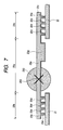
- FIG. 7 is a VII-VII line cross-sectional view in FIG. 5 ;
- FIG. 8 is a cross-sectional view of the electric fuse part of the modification of Embodiment 2;
- FIG. 9 is a top view of the unit structure of the electric fuse part of Embodiment 3.
- FIG. 10 is a X-X line cross-sectional view in FIG. 9 ;
- FIG. 11 is a top view of the unit structure of the electric fuse part of the modification of Embodiment 3;
- FIG. 12 is a XII-XII line cross-sectional view in FIG. 11 ;
- FIG. 13 is a layout drawing of the electric fuse part of Embodiment 3.
- FIG. 14 is a XIV-XIV line cross-sectional view in FIG. 13 ;
- FIG. 15 is a XV-XV line cross-sectional view in FIG. 13 ;
- FIG. 16 is a top view of the electric fuse part of Embodiment 4.
- FIG. 17 is a XVII-XVII line cross-sectional view in FIG. 16 ;
- FIG. 18 is a XVIII-XVIII line cross-sectional view in FIG. 16 ;
- FIG. 19 is a perspective view of the electric fuse part of Embodiment 4.
- FIG. 20 is a perspective view of the electric fuse part of the modification of Embodiment 4.
- FIG. 21 is a layout drawing of the electric fuse part of Embodiment 5.
- FIG. 22 is a XXII-XXII line cross-sectional view in FIG. 21 ;
- FIG. 23 is a XXIII-XXIII line cross-sectional view in FIG. 21 ;
- FIG. 24 is a drawing for explaining the relation between the amount of drifts to a lower-layer wiring layer of the electric fuse part of Embodiment 5, and the amount of drifts to other lower-layer wiring layers of other vias.
- the semiconductor device of an embodiment of the invention is a semiconductor device provided with the electric fuse which may be cut by sending current through a wiring or a via, it may be what kind of thing.
- a semiconductor device is in the tendency that the occupying area of an electric fuse increases as memory space increases.
- the pitch between electric fuses can be made small according to the semiconductor device of this embodiment explained below, the occupying area of an electric fuse group can be reduced.
- the semiconductor device of this embodiment can cut an electric fuse, without having a bad influence on a surrounding structure of an electric fuse, after a semiconductor chip is covered with resin since it has the electric fuse which may be cut with a low current value.
- the semiconductor device of this embodiment is provided with electric fuse parts 10 a and 20 a as shown in FIG. 1 .
- electric fuse part 10 a As shown in FIG. 1 and FIG. 2 , the one side end is connected to conductive part 10 b , and the other side end is connected to conductive part 10 c .
- electric fuse part 20 a As electric fuse part 20 a is shown in FIG. 1 and FIG. 2 , the one side end is connected to conductive part 20 b , and the other side end is connected to conductive part 20 c.
- Conductive parts 10 b and 20 b are connected to a plurality of vias 10 d and a plurality of vias 20 d , respectively.
- a plurality of vias 10 d and a plurality of vias 20 d are connected to wiring layer 11 and wiring layer 21 , respectively.
- conductive parts 10 c and 20 c are connected to a plurality of vias 10 e and a plurality of vias 20 e , respectively.
- a plurality of vias 10 e and a plurality of vias 20 e are connected to wiring layer 12 and wiring layer 22 , respectively.
- Electric fuse part 10 a has a plurality of projecting portions 10 f in which each has the same form as via 10 d or via 10 e .
- Electric fuse part 20 a is connected to a plurality of projecting portions 20 f in which each has the same form as via 20 d or via 20 e.
- the holes where projecting portions 10 f and 20 f , vias 10 d and 20 d , and vias 10 e and 20 e are embedded are simultaneously formed in an interlayer insulating layer in the same etching step.
- a plurality of projecting portions 10 f are formed in the position shifted from the middle position of electric fuse part 10 a , more concretely, in the position distant from via 10 e and near via 10 d .
- a plurality of projecting portions 10 f have the function to make the heat generated in electric fuse part 10 a diffuse. Therefore, as for electric fuse part 10 a , position 150 becomes the highest temperature so that it may be cut in position 150 distant from via 10 d and near via 10 e . Therefore, the interlayer insulating layer located in periphery 100 of position 150 receives the biggest damage.
- a plurality of projecting portions 20 f are formed in the position shifted from the middle position of electric fuse part 20 a , more concretely, in the position distant from via 20 d and near via 20 e .
- a plurality of projecting portions 20 f have the function to make the heat generated in electric fuse part 20 a diffuse. Therefore, as for electric fuse part 20 a , cut position 250 becomes the highest temperature so that it may be cut in cut position 250 distant from via 20 e and near via 20 d . Therefore, the interlayer insulating layer located in periphery 200 of cut position 250 receives the biggest damage.
- Supposing electric fuse parts 10 a and 20 a , conductive parts 10 b , 10 c , 20 b , and 20 c connected to them, vias 10 d , 10 e , 20 d , and 20 e and projecting portions 10 f and 20 f compose a unit structural body, in the semiconductor device of this embodiment, this unit structural body is formed repeatedly. Therefore, projecting portions 10 f and projecting portions 20 f are arranged in the shape of zigzag. Electric fuse part 10 a and electric fuse part 20 a are formed always separating pitch P.
- the pitch between electric fuse parts is restricted by the damaged part of the surrounding interlayer insulating layer of the cut position of an electric fuse part, i.e., the size of periphery 100 and 200 etc. Therefore, when it arranges so that peripheries 100 and 200 may be located in a line in the shape of a straight line, the pitch between electric fuse parts cannot be made small.
- a plurality of projecting portions 10 f and a plurality of projecting portions 20 f are arranged in the shape of zigzag so that peripheries 100 and 200 may be arranged in the shape of zigzag seeing in plan view.
- pitch P between electric fuse part 10 a and electric fuse part 20 a can be reduced as much as possible.
- a plurality of projecting portions 10 f and 20 f which consist of a plurality of vias are formed only in electric fuse part 10 a and 20 a lower part. Since projecting portions 10 f and 20 f are formed in the same layer as vias 10 d , 10 e , 20 d , and 20 e in the same step according to this, there are not an increase in the occupation ratio of the structural body which forms electric fuse parts 10 a and 20 a , and an increase in the step for manufacturing electric fuse parts 10 a and 20 a.
- FIG. 5-FIG . 7 the semiconductor device of an embodiment of the invention is explained using FIG. 5-FIG . 7 .
- the structure of the semiconductor device of this embodiment is almost the same as the structure of the semiconductor device of Embodiment 1. Therefore, in the semiconductor device of this embodiment, the same referential mark as the referential mark used in Embodiment 1 is attached to the part which has the same structure and the same function as a semiconductor device of Embodiment 1.
- the semiconductor device of this embodiment differs from the semiconductor device of Embodiment 1 in the point that wiring parts 10 g and 20 g are respectively formed in electric fuse part 10 a and 20 a lower part instead of a plurality of projecting portions 10 f and 20 f of Embodiment 1.
- projecting portion 10 g which consist of one lump have bigger volume than the whole of a plurality of projecting portions 10 f . Therefore, the radiation efficiency of a projecting portion increases.
- the current density of projecting portions 10 g and 20 g is lower than the current density of a plurality of projecting portions 10 f and 20 f respectively. Therefore, the Joule's heat itself which raises the temperature of electric fuse parts 10 a and 20 a is reduced. As a result, the bad influence to peripheries 100 and 200 of electric fuse parts 10 a and 20 a is inhibited.
- projecting portion 10 h which projects in both sides of electric fuse part 10 a may be formed. Also by this, the same effect as the effect acquired by projecting portions 10 f can be acquired. In this case, although not illustrated, the same projecting portion 20 h as projecting portion 10 h has projected from the both side surfaces of electric fuse part 20 a.
- electric fuse part 30 a In electric fuse part 30 a , the one side end is connected to wiring layer 30 b , and the other side end is connected to wiring layer 30 c .
- a plurality of vias 30 e are connected to wiring layer 30 c .
- Wiring layer 30 b , electric fuse part 30 a , wiring layer 30 c , and via 30 e are formed in one.
- Lower-layer wiring layer 31 is connected to via 30 e .
- Via 32 a is connected to wiring layer 30 b .
- Via 32 a is formed in one with the upper wiring layer 32 .
- wiring layer 30 b and the upper wiring layer 32 are connected by only one via 32 a.
- the cross-section area of via 32 a is smaller than the cross-section area of a plurality of vias 30 e . Therefore, the calorific value of via 32 a is larger than the calorific value of a plurality of vias 30 e.
- temperature of electric fuse part 30 a near the via 32 a can be made higher than the temperature near a plurality of vias 30 e . Therefore, cut position 350 and its periphery 300 can be inclined and formed in the via 32 a side from the middle position of electric fuse part 30 a.
- FIG. 13-FIG . 15 the structure of the electric fuse part of the semiconductor device of this embodiment is explained using FIG. 13-FIG . 15 .
- the unit structure of an electric fuse part is different from the unit structure of an electric fuse part shown in FIG. 9-FIG . 12
- the unit structure of an electric fuse part shown in FIG. 9-FIG . 12 may be used.
- electric fuse part 30 a As shown in FIG. 13 and FIG. 14 , the one side end is connected to wiring layer 30 b , and the other side end is connected to wiring layer 30 c .
- Via 32 a is connected to wiring layer 30 b .
- Via 32 a is formed in one with the upper wiring layer 32 .
- Wiring layer 30 c is connected to a plurality of vias 30 e formed in one.
- a plurality of vias 30 e are connected to lower-layer wiring layer 31 .
- a plurality of projecting portions 30 f have projected in the lower part from electric fuse part 30 a .
- a plurality of projecting portions 30 f are formed in the position which inclined toward the wiring layer 30 c side rather than the middle position of electric fuse part 30 a.
- the cross-section area of via 32 a is smaller than the cross-section area of a plurality of vias 30 e . Therefore, the calorific value of via 32 a is larger than the calorific value of a plurality of vias 30 e . Therefore, according to the semiconductor device of this embodiment, temperature of electric fuse part 30 a near the via 32 a can be made higher than the temperature near a plurality of vias 30 e . Therefore, cut position 350 and its periphery 300 can be inclined and formed in the via 32 a side from the middle position of electric fuse part 30 a.
- a part of upper wiring layer 32 of the position connected to via 32 a is thinner than other portions. Therefore, the resistance of the upper wiring layer 32 near the position connected to via 32 a is smaller than the resistance of other portions. According to this, it is possible to heighten the heater effect near the via 32 a more.
- electric fuse part 40 a As shown in FIG. 13 and FIG. 15 , the one side end is connected to wiring layer 40 b , and the other side end is connected to wiring layer 40 c . Via 42 a is connected to wiring layer 40 c . Via 42 a is formed in one with the upper wiring layer 42 . Wiring layer 40 b is formed in one with a plurality of vias 40 e . A plurality of vias 40 e are connected to lower-layer wiring layer 41 . A plurality of projecting portions 40 f have projected in the lower part from electric fuse part 40 a . A plurality of projecting portions 40 f are formed in the position which inclined toward the wiring layer 40 b side rather than the middle position of electric fuse part 40 a.
- the cross-section area of via 42 a is smaller than the cross-section area of a plurality of vias 40 e . Therefore, the calorific value of via 42 a is larger than the calorific value of a plurality of vias 40 e . Therefore, according to the semiconductor device of this embodiment, temperature of electric fuse part 40 a near the via 42 a can be made higher than the temperature near a plurality of vias 40 e . Therefore, cut position 450 and its periphery 400 can be inclined and formed in the via 42 a side from the middle position of electric fuse part 40 a.
- the upper wiring layer 42 near the position connected to via 42 a is thinner than other portions. Therefore, the resistance of the upper wiring layer 42 near the position connected to via 42 a is smaller than the resistance of other portions. According to this, it is possible to heighten the heater effect near the via 42 a more.
- the fuse unit shown in FIG. 14 and FIG. 15 is formed repeatedly.
- a plurality of projecting portions 30 f and a plurality of projecting portions 40 f are arranged in the shape of zigzag. Therefore, cut position 350 (periphery 300 ) of electric fuse part 30 a and cut position 450 (periphery 400 ) of electric fuse part 40 a will also be arranged in the shape of zigzag. Therefore, by the same effect as the effect acquired by the semiconductor device of Embodiment 1 and 2, it becomes possible to reduce pitch P between electric fuse part 30 a and electric fuse part 40 a .
- lower-layer wiring layer 41 and the upper wiring layer 32 are formed so that they may overlap in a plan view as shown in FIG. 13
- lower-layer wiring layer 31 and the upper wiring layer 42 are formed so that they may overlap in a plan view. Therefore, the restrictions which pitch P between lower-layer wiring layers and pitch P between the upper wiring layers receive by each width of the upper wiring layers 32 and 42 and lower-layer wiring layers 31 and 41 are eased.
- cut positions 350 and 450 can be zigzag formed according to a difference of the cross-section area between via 32 a and a plurality of vias 30 e , and a difference of the cross-section area between via 42 a and a plurality of vias 40 e .
- the width of upper wiring layer 32 near the via 32 a and upper wiring layer 42 near the via 42 a is smaller than other portions.
- cut positions 350 and 450 can be formed zigzag.
- a difference of the cross-section area between vias 32 a and 42 a and a plurality of vias 30 e and 40 e is an example of a difference of the resistance between vias 32 a and 42 a and a plurality of vias 30 e and 40 e .
- a difference of the resistance between vias 32 a and 42 a and a plurality of vias 30 e and 40 e may be brought about by other structures.
- the via vertically prolonged to a semiconductor substrate functions as an electric fuse part.
- Electric fuse part 1070 consists of a via prolonged in the vertical direction to the main surface of a semiconductor substrate in the semiconductor device of this embodiment.
- the one side end is connected to wiring layer 1060 of the same width as electric fuse part 1070
- the other side end is connected to wiring layer 1080 of the same width as electric fuse part 1070 .
- Wiring layer 1050 which has bigger width than wiring layer 1060 is connected to wiring layer 1060 .
- wiring layer 1050 , wiring layer 1060 , and electric fuse part 1070 are formed in one.
- Wiring layer 1080 is connected to wiring layer 1090 which has bigger width than wiring layer 1080 .
- Wiring layers 1080 and 1090 are formed in one.
- electric fuse part 1170 As shown in FIG. 16-FIG . 19 , the one side end is connected to wiring layer 1160 of the same width as electric fuse part 1170 , and the other side end is connected to wiring layer 1180 of the same width as electric fuse part 1170 .
- Wiring layer 1150 which has bigger width than wiring layer 1160 is connected to wiring layer 1160 .
- wiring layer 1150 , wiring layer 1160 , and electric fuse part 1170 are formed in one.
- Wiring layer 1180 is connected to wiring layer 1190 which has bigger width than wiring layer 1180 .
- Wiring layers 1180 and 1190 are formed in one.
- the fuse unit shown in FIG. 17 and FIG. 18 is formed repeatedly. Seeing in plan view, electric fuse part 1070 and electric fuse part 1170 are arranged in the shape of zigzag. Therefore, the cut position of electric fuse part 1070 and the cut position of electric fuse part 1170 will be arranged in the shape of zigzag seeing in plan view. Therefore, by the same effect as the effect acquired by the semiconductor device of Embodiments 1-3, it becomes possible to reduce pitch P between electric fuse part 1070 and electric fuse part 1170 .
- wiring layer 1060 and wiring layer 1160 may be quite long in the comparison with electric fuse parts 1070 and 1170 , as shown in FIG. 20 .
- FIG. 21-FIG . 24 the semiconductor device of an embodiment of the invention is explained using FIG. 21-FIG . 24 .
- the semiconductor device of this embodiment has the upper wiring layer 1250 prolonged in parallel to the main surface of a semiconductor substrate, and the upper wiring layer 1260 which is formed in the upper wiring layer 1250 in one in the same layer as the upper wiring layer 1250 , and has width smaller than the upper wiring layer 1250 .
- Electric fuse part 1270 prolonged toward a lower part from the upper wiring layer 1260 is formed in the upper wiring layer 1260 in one.
- Lower-layer wiring layer 1280 is connected to the lower end of electric fuse part 1270 .
- lower-layer wiring layer 1290 which has bigger width than lower-layer wiring layer 1280 is formed in lower-layer wiring layer 1280 in one.
- It has the upper wiring layer 1350 prolonged in parallel to the main surface of a semiconductor substrate, and the upper wiring layer 1360 which is formed in the upper wiring layer 1350 in one in the same layer as the upper wiring layer 1350 , and has width smaller than the upper wiring layer 1350 .
- Electric fuse part 1370 prolonged toward a lower part from the upper wiring layer 1360 is formed in the upper wiring layer 1360 in one.
- Lower-layer wiring layer 1380 is connected to the lower end of electric fuse part 1370 .
- Lower-layer wiring layer 1390 which has bigger width than lower-layer wiring layer 1380 is formed in lower-layer wiring layer 1380 in one in the same layer as lower-layer wiring layer 1380 .
- the structure of the above semiconductor devices of this embodiment is the same as the structure of the semiconductor device of Embodiment 4. That is, electric fuse parts 1270 and 1370 are arranged in the shape of zigzag seeing in plan view.
- the problem of the semiconductor device of Embodiment 4 is explained. Like the semiconductor device of above-mentioned Embodiment 4, in order to operate a via as an electric fuse part, it is required to prevent the inconvenience that a cut section will be formed in the wiring layer connected to the via. Therefore, the structure where the temperature of a via becomes higher than the temperature of other parts by electrical connection must be formed. Therefore, the width of the wiring layer connected to the via must be equal to or more than the width of an electric fuse part.
- the width of the wiring layer directly connected to a via is desirable to be small in a certain degree as shown in FIG. 16 .
- the width of the wiring layer directly connected to a via it is more preferred that it is the same as that of the width of a via. This is because lowering of the temperature of the portion near the via can be suppressed.
- the length of the wiring layer with small width connected to the via is about 1 ⁇ 3 ⁇ m.
- the bottom of electric fuse part 1270 and electric fuse part 1370 has protruded from lower-layer wiring layers 1280 and 1380 , respectively.
- the contact area between electric fuse part 1270 and lower-layer wiring layer 1280 can be made smaller than the area of the cross section of electric fuse part 1270 . It becomes possible to make the contact area between electric fuse part 1370 and lower-layer wiring layer 1380 smaller than the area of the cross section of electric fuse part 1370 .
- each current density of electric fuse parts 1270 and 1370 can be improved locally. Therefore, each calorific value of electric fuse parts 1270 and 1370 can be enlarged locally. Therefore, it becomes possible to produce cutting surely in each of electric fuse parts 1270 and 1370 .
- each amount of drifts from lower-layer wiring layers 1280 and 1380 of electric fuse parts 1270 and 1370 of this embodiment differs clearly from the amount of drifts of central line C 4 or C 5 of other vias 1420 formed in the same layer in the same step as electric fuse parts 1270 and 1370 , and central line C 1 or C 2 of other lower-layer wiring layers 1450 as shown in FIG. 24 .
- each amount ⁇ X of drifts from central line C 3 of lower-layer wiring layers 1280 and 1380 of central line C 6 of electric fuse parts 1270 and 1370 is larger than 1 ⁇ 3 of each width W of lower-layer wiring layers 1280 and 1380 . According to this, in vias 1270 and 1370 , cutting can be generated surely.
Landscapes
- Design And Manufacture Of Integrated Circuits (AREA)
- Semiconductor Integrated Circuits (AREA)
Abstract
Description
Claims (35)
Priority Applications (2)
| Application Number | Priority Date | Filing Date | Title |
|---|---|---|---|
| US12/869,323 US8487402B2 (en) | 2007-01-10 | 2010-08-26 | Semiconductor device |
| US12/878,977 US8487403B2 (en) | 2007-01-10 | 2010-09-09 | Semiconductor device |
Applications Claiming Priority (2)
| Application Number | Priority Date | Filing Date | Title |
|---|---|---|---|
| JP2007002685A JP5230105B2 (en) | 2007-01-10 | 2007-01-10 | Semiconductor device |
| JP2007-002685 | 2007-01-10 |
Related Child Applications (1)
| Application Number | Title | Priority Date | Filing Date |
|---|---|---|---|
| US12/869,323 Division US8487402B2 (en) | 2007-01-10 | 2010-08-26 | Semiconductor device |
Publications (2)
| Publication Number | Publication Date |
|---|---|
| US20080164969A1 US20080164969A1 (en) | 2008-07-10 |
| US7808076B2 true US7808076B2 (en) | 2010-10-05 |
Family
ID=39593766
Family Applications (3)
| Application Number | Title | Priority Date | Filing Date |
|---|---|---|---|
| US11/958,360 Active 2028-04-04 US7808076B2 (en) | 2007-01-10 | 2007-12-17 | Semiconductor device |
| US12/869,323 Expired - Fee Related US8487402B2 (en) | 2007-01-10 | 2010-08-26 | Semiconductor device |
| US12/878,977 Expired - Fee Related US8487403B2 (en) | 2007-01-10 | 2010-09-09 | Semiconductor device |
Family Applications After (2)
| Application Number | Title | Priority Date | Filing Date |
|---|---|---|---|
| US12/869,323 Expired - Fee Related US8487402B2 (en) | 2007-01-10 | 2010-08-26 | Semiconductor device |
| US12/878,977 Expired - Fee Related US8487403B2 (en) | 2007-01-10 | 2010-09-09 | Semiconductor device |
Country Status (2)
| Country | Link |
|---|---|
| US (3) | US7808076B2 (en) |
| JP (1) | JP5230105B2 (en) |
Cited By (2)
| Publication number | Priority date | Publication date | Assignee | Title |
|---|---|---|---|---|
| US20090280636A1 (en) * | 2008-05-09 | 2009-11-12 | Hsu Louis L | Methods of fabricating interconnect structures containing various capping materials for electrical fuse and other related applications |
| US20130168807A1 (en) * | 2008-05-09 | 2013-07-04 | International Business Machines Corporation | Interconnect structure containing various capping materials for electrical fuse and other related applications, and design structure thereof |
Families Citing this family (11)
| Publication number | Priority date | Publication date | Assignee | Title |
|---|---|---|---|---|
| JP5331408B2 (en) * | 2008-08-11 | 2013-10-30 | ルネサスエレクトロニクス株式会社 | Semiconductor device |
| JP5422231B2 (en) * | 2008-08-13 | 2014-02-19 | 株式会社東芝 | Nonvolatile semiconductor memory device and manufacturing method thereof |
| US8855067B2 (en) | 2010-04-02 | 2014-10-07 | Marvell World Trade Ltd. | Multi-user communication group management and signaling |
| JP5581520B2 (en) * | 2010-04-08 | 2014-09-03 | ルネサスエレクトロニクス株式会社 | Semiconductor device and manufacturing method thereof |
| US8912626B2 (en) * | 2011-01-25 | 2014-12-16 | International Business Machines Corporation | eFuse and method of fabrication |
| US20120286390A1 (en) * | 2011-05-11 | 2012-11-15 | Kuei-Sheng Wu | Electrical fuse structure and method for fabricating the same |
| US8847350B2 (en) * | 2012-08-30 | 2014-09-30 | Taiwan Semiconductor Manufacturing Company, Ltd. | Metal-via fuse |
| KR102096614B1 (en) * | 2013-10-11 | 2020-04-03 | 삼성전자주식회사 | e-fuse structure of a semiconductor device |
| US9401258B2 (en) * | 2014-07-30 | 2016-07-26 | Taiwan Semiconductor Manufacturing Company, Ltd. | Fuse structure |
| CN110998777B (en) * | 2017-08-30 | 2022-09-20 | 三菱电机株式会社 | Power conversion device |
| CN113013140A (en) * | 2021-04-28 | 2021-06-22 | 上海华力微电子有限公司 | Layout structure of efuse fuse |
Citations (5)
| Publication number | Priority date | Publication date | Assignee | Title |
|---|---|---|---|---|
| JP2001024063A (en) | 1999-06-09 | 2001-01-26 | Internatl Business Mach Corp <Ibm> | Fuse structure and method for forming the same |
| JP2001230325A (en) | 2000-02-16 | 2001-08-24 | Oki Electric Ind Co Ltd | Metal fuse, manufacturing method thereof and mask |
| US20050274966A1 (en) | 2004-06-10 | 2005-12-15 | Matsushita Electric Industrial Co., Ltd. | Fuse and write method for fuse |
| US20050285224A1 (en) | 2004-06-29 | 2005-12-29 | Matsushita Electric Industrial Co., Ltd. | Semiconductor device and manufacturing method thereof |
| US20060278953A1 (en) * | 2005-06-14 | 2006-12-14 | Oki Electric Industry Co., Ltd. | Semiconductor memory device |
Family Cites Families (3)
| Publication number | Priority date | Publication date | Assignee | Title |
|---|---|---|---|---|
| JP2000286341A (en) * | 1999-03-31 | 2000-10-13 | Nec Corp | Fuse structure of semiconductor device |
| JP2004228369A (en) * | 2003-01-23 | 2004-08-12 | Sony Corp | Semiconductor device and fuse blowing method |
| JP2006310277A (en) * | 2005-03-29 | 2006-11-09 | Mitsubishi Materials Corp | Chip type fuse |
-
2007
- 2007-01-10 JP JP2007002685A patent/JP5230105B2/en not_active Expired - Fee Related
- 2007-12-17 US US11/958,360 patent/US7808076B2/en active Active
-
2010
- 2010-08-26 US US12/869,323 patent/US8487402B2/en not_active Expired - Fee Related
- 2010-09-09 US US12/878,977 patent/US8487403B2/en not_active Expired - Fee Related
Patent Citations (9)
| Publication number | Priority date | Publication date | Assignee | Title |
|---|---|---|---|---|
| JP2001024063A (en) | 1999-06-09 | 2001-01-26 | Internatl Business Mach Corp <Ibm> | Fuse structure and method for forming the same |
| US6252292B1 (en) | 1999-06-09 | 2001-06-26 | International Business Machines Corporation | Vertical electrical cavity-fuse |
| JP2001230325A (en) | 2000-02-16 | 2001-08-24 | Oki Electric Ind Co Ltd | Metal fuse, manufacturing method thereof and mask |
| US6566729B1 (en) | 2000-02-16 | 2003-05-20 | Oki Electric Industry Co., Ltd. | Semiconductor device including laser-blown links |
| US20050274966A1 (en) | 2004-06-10 | 2005-12-15 | Matsushita Electric Industrial Co., Ltd. | Fuse and write method for fuse |
| US20050285224A1 (en) | 2004-06-29 | 2005-12-29 | Matsushita Electric Industrial Co., Ltd. | Semiconductor device and manufacturing method thereof |
| JP2006013338A (en) | 2004-06-29 | 2006-01-12 | Matsushita Electric Ind Co Ltd | Semiconductor device and manufacturing method thereof |
| JP2006108413A (en) | 2004-10-06 | 2006-04-20 | Matsushita Electric Ind Co Ltd | Fuse and fuse writing method |
| US20060278953A1 (en) * | 2005-06-14 | 2006-12-14 | Oki Electric Industry Co., Ltd. | Semiconductor memory device |
Cited By (4)
| Publication number | Priority date | Publication date | Assignee | Title |
|---|---|---|---|---|
| US20090280636A1 (en) * | 2008-05-09 | 2009-11-12 | Hsu Louis L | Methods of fabricating interconnect structures containing various capping materials for electrical fuse and other related applications |
| US20130168807A1 (en) * | 2008-05-09 | 2013-07-04 | International Business Machines Corporation | Interconnect structure containing various capping materials for electrical fuse and other related applications, and design structure thereof |
| US8692375B2 (en) * | 2008-05-09 | 2014-04-08 | International Business Machines Corporation | Interconnect structure containing various capping materials for programmable electrical fuses |
| US8772156B2 (en) | 2008-05-09 | 2014-07-08 | International Business Machines Corporation | Methods of fabricating interconnect structures containing various capping materials for electrical fuse and other related applications |
Also Published As
| Publication number | Publication date |
|---|---|
| JP5230105B2 (en) | 2013-07-10 |
| US20100320562A1 (en) | 2010-12-23 |
| US20080164969A1 (en) | 2008-07-10 |
| US8487402B2 (en) | 2013-07-16 |
| JP2008171953A (en) | 2008-07-24 |
| US8487403B2 (en) | 2013-07-16 |
| US20110006392A1 (en) | 2011-01-13 |
Similar Documents
| Publication | Publication Date | Title |
|---|---|---|
| US7808076B2 (en) | Semiconductor device | |
| JP4795631B2 (en) | Semiconductor device | |
| US7795699B2 (en) | Semiconductor device | |
| US8421186B2 (en) | Electrically programmable metal fuse | |
| US7732892B2 (en) | Fuse structures and integrated circuit devices | |
| KR20090023939A (en) | Electrical fuse elements | |
| KR101993854B1 (en) | Antifuse of semiconductor device, module and system having the semiconductor device and manufacturing method for the antifuse | |
| JP4861060B2 (en) | Semiconductor device and electrical fuse cutting method | |
| KR20060134826A (en) | Melting method of semiconductor device and fuse | |
| CN109786359B (en) | Semiconductor device and method of forming the same | |
| JP2003163269A (en) | Rectangular contacts used as low voltage fuse elements | |
| US7645645B2 (en) | Electrically programmable fuse structures with terminal portions residing at different heights, and methods of fabrication thereof | |
| JP5430879B2 (en) | Electrical fuse, semiconductor device, and electrical fuse cutting method | |
| JP5638188B2 (en) | Semiconductor device | |
| JP2008526007A (en) | Antifuse cell and manufacturing method thereof | |
| US8080861B2 (en) | Semiconductor device | |
| JP5103666B2 (en) | Semiconductor device | |
| EP4089727A1 (en) | Semiconductor structure and formation method therefor, and fusing method for laser fuse | |
| JP5547779B2 (en) | Semiconductor device | |
| US9006861B2 (en) | Integrated circuit device | |
| CN101651127A (en) | Semiconductor device | |
| JP2002353311A (en) | Semiconductor device and fuse cutting method | |
| KR100652418B1 (en) | Semiconductor device with improved fuseline structure | |
| JP2012043905A (en) | Semiconductor device | |
| US20100187638A1 (en) | Anti-fuse cell and its manufacturing process |
Legal Events
| Date | Code | Title | Description |
|---|---|---|---|
| AS | Assignment |
Owner name: RENESAS TECHNOLOGY CORP., JAPAN Free format text: ASSIGNMENT OF ASSIGNORS INTEREST;ASSIGNORS:KONO, KAZUSHI;IWAMOTO, TAKESHI;KATO, HISAYUKI;AND OTHERS;REEL/FRAME:020260/0296 Effective date: 20070820 |
|
| AS | Assignment |
Owner name: RENESAS ELECTRONICS CORPORATION, JAPAN Free format text: CHANGE OF NAME;ASSIGNOR:NEC ELECTRONICS CORPORATION;REEL/FRAME:024864/0635 Effective date: 20100401 Owner name: NEC ELECTRONICS CORPORATION, JAPAN Free format text: MERGER;ASSIGNOR:RENESAS TECHNOLOGY CORP.;REEL/FRAME:024879/0190 Effective date: 20100401 |
|
| STCF | Information on status: patent grant |
Free format text: PATENTED CASE |
|
| FEPP | Fee payment procedure |
Free format text: PAYOR NUMBER ASSIGNED (ORIGINAL EVENT CODE: ASPN); ENTITY STATUS OF PATENT OWNER: LARGE ENTITY |
|
| FPAY | Fee payment |
Year of fee payment: 4 |
|
| AS | Assignment |
Owner name: RENESAS ELECTRONICS CORPORATION, JAPAN Free format text: CHANGE OF ADDRESS;ASSIGNOR:RENESAS ELECTRONICS CORPORATION;REEL/FRAME:044928/0001 Effective date: 20150806 |
|
| MAFP | Maintenance fee payment |
Free format text: PAYMENT OF MAINTENANCE FEE, 8TH YEAR, LARGE ENTITY (ORIGINAL EVENT CODE: M1552) Year of fee payment: 8 |
|
| MAFP | Maintenance fee payment |
Free format text: PAYMENT OF MAINTENANCE FEE, 12TH YEAR, LARGE ENTITY (ORIGINAL EVENT CODE: M1553); ENTITY STATUS OF PATENT OWNER: LARGE ENTITY Year of fee payment: 12 |