US7764113B2 - Output circuit - Google Patents
Output circuit Download PDFInfo
- Publication number
- US7764113B2 US7764113B2 US12/169,462 US16946208A US7764113B2 US 7764113 B2 US7764113 B2 US 7764113B2 US 16946208 A US16946208 A US 16946208A US 7764113 B2 US7764113 B2 US 7764113B2
- Authority
- US
- United States
- Prior art keywords
- voltage
- output
- terminal
- transistor
- capacitor
- Prior art date
- Legal status (The legal status is an assumption and is not a legal conclusion. Google has not performed a legal analysis and makes no representation as to the accuracy of the status listed.)
- Expired - Fee Related, expires
Links
Images


Classifications
-
- H—ELECTRICITY
- H03—ELECTRONIC CIRCUITRY
- H03F—AMPLIFIERS
- H03F1/00—Details of amplifiers with only discharge tubes, only semiconductor devices or only unspecified devices as amplifying elements
- H03F1/02—Modifications of amplifiers to raise the efficiency, e.g. gliding Class A stages, use of an auxiliary oscillation
- H03F1/0205—Modifications of amplifiers to raise the efficiency, e.g. gliding Class A stages, use of an auxiliary oscillation in transistor amplifiers
- H03F1/0211—Modifications of amplifiers to raise the efficiency, e.g. gliding Class A stages, use of an auxiliary oscillation in transistor amplifiers with control of the supply voltage or current
-
- H—ELECTRICITY
- H03—ELECTRONIC CIRCUITRY
- H03F—AMPLIFIERS
- H03F2200/00—Indexing scheme relating to amplifiers
- H03F2200/504—Indexing scheme relating to amplifiers the supply voltage or current being continuously controlled by a controlling signal, e.g. the controlling signal of a transistor implemented as variable resistor in a supply path for, an IC-block showed amplifier
Definitions
- the present invention relates to an output circuit for a series regulator or a power amplifier, and more particularly, to an output circuit in which an NPN transistor or an NMOS transistor is used as an output transistor.
- a PMOS transistor is frequently used as an output transistor in a series regulator as typified by an LDO (low drop out regulator) or a power amplifier that supplies a controlled voltage to a load circuit.
- the PMOS transistor has a problem that its chip area is larger than that of an NMOS transistor having the same current capacity.
- FIG. 4 The circuit configuration of the series regulator disclosed in Japanese Patent Application Laid-Open Publication No. Hei 3-204012 is shown in FIG. 4 .
- numeral 1 designates an input terminal. An input voltage Vin is applied to this input terminal 1 .
- Numeral 2 designates an output terminal. This output terminal 2 supplies an output voltage Vout to a load 3 .
- NMOS transistor 4 designates an NMOS transistor serving as an output transistor. This NMOS transistor 4 is connected between the input terminal 1 and the output terminal 2 .
- Numeral 5 designates an amplifier. This amplifier 5 supplies a drive voltage to the gate terminal of the NMOS transistor 4 .
- Numeral 6 designates a reference voltage generating circuit. This reference voltage generating circuit 6 generates a reference voltage Vref and applies the generated reference voltage Vref to the non-inverting input terminal (+) of the amplifier 5 .
- Numeral 7 designates a resistor pair consisting of a series circuit of two voltage-dividing resistors. This resistor pair 7 divides the output voltage Vout, and the divided voltage is applied to the inverting input terminal ( ⁇ ) of the amplifier 5 .
- Numeral 9 designates a charge pump circuit. This charge pump circuit 9 generates a voltage stepped up from the input voltage Vin, and this stepped-up voltage is supplied to the amplifier 5 as a power supply voltage.
- the charge pump circuit 9 operates, and the voltage stepped up from the input voltage Vin is supplied to the amplifier 5 .
- the NMOS transistor 4 is driven by the amplifier 5 , and the output voltage Vout is output from the output terminal 2 .
- the output voltage Vout is negatively fed back to the amplifier 5 through the resistor pair 7 .
- the amplifier 5 controls the NMOS transistor 4 so that the divided voltage of the output voltage Vout, being output from the resistor pair 7 , becomes equal to the reference voltage Vref of the reference voltage generating circuit 6 .
- the output voltage Vout is controlled so as to be stabilized.
- the amplifier 5 is biased by the voltage stepped up from the input voltage Vin. Hence, the amplifier 5 can supply a sufficiently high gate voltage to the NMOS transistor 4 .
- the conventional charge pump circuit 9 described above is connected only to the input voltage Vin, the ground and the amplifier 5 .
- the stepped-up voltage with reference to the input voltage is used as the power supply voltage for the amplifier 5 .
- the voltage is excessively high as the power supply voltage for the control drive circuit, and power consumption increases.
- the drive voltage to the NMOS transistor 4 serving as an output transistor can be obtained securely.
- the voltage stepped up by the charge pump circuit 9 is high, and the power consumption in the amplifier 5 increases.
- An object of the present invention is to provide an output circuit applied to a series regulator or a power amplifier, capable of suppressing the increase in power consumption while securely obtaining the drive voltage for an output transistor even when the output transistor is an NMOS transistor or an NPN transistor.
- a first output circuit comprises an output transistor having one main terminal to which an input voltage is input, the other main terminal from which an output voltage is output and a control terminal, wherein a drive voltage being equal to or higher than the drive threshold voltage with reference to the potential of the other main terminal is applied to the control terminal, whereby the impedance between the one main terminal and the other main terminal can be controlled; a control drive circuit for supplying the drive voltage to the control terminal of the output transistor to control the output voltage from the other main terminal of the output transistor; and a charge pump circuit, configured so as to output a predetermined voltage being equal to or higher than the drive threshold voltage with reference to the potential of the other main terminal of the output transistor, for supplying the power supply voltage obtained by adding the predetermined voltage being equal to or higher than the drive threshold voltage to the output voltage from the other main terminal of the output transistor.
- a second output circuit comprises an output transistor having one main terminal to which an input voltage is input, the other main terminal from which an output voltage is output and a control terminal, wherein a drive voltage being equal to or higher than the drive threshold voltage with reference to the potential of the other main terminal is applied to the control terminal, whereby the impedance between the one main terminal and the other main terminal can be controlled; a control drive circuit for supplying the drive voltage to the control terminal of the output transistor to control the output voltage from the other main terminal of the output transistor; and a charge pump circuit, configured so as to output a voltage with reference to the potential of the one main terminal of the output transistor, for carrying out control so that the power supply voltage supplied to the control drive circuit is the voltage obtained by adding a predetermined voltage being equal to or higher than the drive threshold voltage to the output voltage from the other main terminal of the output transistor.
- the power supply voltage supplied to the control drive circuit for driving the output transistor becomes the voltage obtained by adding a voltage being equal to or higher than the drive threshold voltage of the output transistor to the output voltage from the other main terminal of the output transistor, whereby the drive voltage for the output transistor can be obtained securely. Furthermore, since the drive voltage is not affected by the difference between the input and output voltages of the output transistor, the drive voltage can be set at the required minimum voltage being equal to or higher than the drive threshold voltage of the output transistor. It is thus possible to suppress the power consumption in the control drive circuit while the drive voltage for the output transistor is obtained securely.
- the output transistor is preferably, for example, an NMOS transistor or an NPN transistor.
- the control drive circuit has a differential amplifier, that the output voltage from the other main terminal of the output transistor or a voltage with reference to the output voltage from the other main terminal of the output transistor is input to one of the input terminals of the differential amplifier, that a reference voltage or a voltage to be amplified is input to the other input terminal of the differential amplifier, and that the output voltage of the differential amplifier is supplied to the control terminal of the output transistor as the drive voltage.
- the charge pump circuit comprises a DC power supply for generating a predetermined voltage, a first capacitor, a first switching circuit for charging the first capacitor from the DC power supply, a second capacitor, one terminal of which is connected to the other main terminal of the output transistor, and a second switching circuit for charging the second capacitor from the first capacitor, and that the voltage appearing at the other terminal of the second capacitor is supplied to the control drive circuit.
- the predetermined voltage generated by the DC power supply is set at a voltage equal to or higher than the drive threshold voltage of the output transistor.
- the charge pump circuit comprises a DC power supply for generating a predetermined voltage, a first capacitor, a first switching circuit for charging the first capacitor from the DC power supply, a second capacitor, one terminal of which is connected to the one main terminal of the output transistor, and a second switching circuit for charging the second capacitor from the first capacitor, and that the voltage generated at the other terminal of the second capacitor is supplied to the control drive circuit.
- the predetermined voltage generated by the DC power supply is set at the voltage obtained by adding a voltage equal to or higher than the drive threshold voltage of the output transistor to the output voltage from the other main terminal of the output transistor and by subtracting the input voltage to the one main terminal of the output transistor from the sum of the addition.
- the DC power supply has a differential amplifier, a transistor and a third capacitor, that the voltage appearing at the other terminal of the second capacitor or a voltage with reference to the voltage appearing at the other terminal of the second capacitor is input to one of the input terminals of the differential amplifier, that the reference voltage is input to the other input terminal of the differential amplifier, that the output voltage of the differential amplifier is supplied to the control terminal of the transistor, that one main terminal of the transistor is connected to the one main terminal of the output transistor, that the other main terminal of the transistor is connected to one terminal of the third capacitor, that the other terminal of the third capacitor is grounded, and that the voltage is output from across the terminals of the third capacitor.
- a charge pump is formed such that the power supply voltage of the control drive circuit, such as an amplifier for driving the output transistor, becomes the voltage obtained by adding the voltage being equal to or higher than the drive threshold voltage of the output transistor to the output voltage.
- the power supply voltage should only be the voltage obtained by adding a voltage higher than the drive threshold voltage of the NMOS transistor by 1 to 2 V to the voltage at the source terminal (the other main terminal) of the NMOS transistor, i.e., the output voltage thereof.
- the predetermined drive voltage can be supplied stably to the control terminal of the output transistor regardless of the input/output voltages. For this reason, even when the NMOS transistor is used as the output transistor in a series regulator or a power amplifier, the drive voltage for the output transistor is obtained securely by the charge pump circuit and can be suppressed to the required minimum voltage, and the power consumption in the control drive circuit such as an amplifier can be suppressed.
- FIG. 1 is a circuit diagram showing the configuration of a series regulator having an output circuit according to Embodiment 1 of the present invention
- FIG. 2 is a circuit diagram showing the configuration of a power amplifier having an output circuit according to Embodiment 2 of the present invention
- FIG. 3 is a circuit diagram showing the configuration of a series regulator having an output circuit according to Embodiment 3 of the present invention
- FIG. 4 is a circuit diagram showing the configuration of the series regulator having the conventional output circuit.
- FIG. 1 is a circuit diagram showing the configuration of a series regulator having an output circuit according to Embodiment 1 of the present invention.
- numeral 1 designates an input terminal. An input voltage Vin is applied to this input terminal 1 .
- Numeral 2 designates an output terminal. This output terminal 2 supplies an output voltage Vout to a load 3 .
- Numeral 4 designates an NMOS transistor serving as an output transistor.
- the drain terminal serving as one of the main terminals of this NMOS transistor 4 is connected to the input terminal 1 , and the source terminal serving as the other main terminal thereof is connected to the output terminal 2 .
- Numeral 5 designates an amplifier. This amplifier 5 supplies a drive voltage to the gate terminal serving as the control terminal of the NMOS transistor 4 .
- Numeral 6 designates a reference voltage generating circuit. This reference voltage generating circuit 6 generates a reference voltage Vref and applies the generated reference voltage Vref to the non-inverting input terminal (+) of the amplifier 5 .
- Numeral 7 designates a resistor pair consisting of two voltage-dividing resistors connected in series. This resistor pair 7 divides the output voltage Vout, and the divided voltage is applied to the inverting input terminal ( ⁇ ) of the amplifier 5 .
- the circuit may be configured such that the output voltage Vout is directly applied to the inverting input terminal ( ⁇ ) of the amplifier 5 , without being divided.
- Numeral 8 designates a charge pump circuit. This charge pump circuit 8 supplies a power supply voltage to the amplifier 5 .
- the charge pump circuit 8 comprises a DC power supply 10 for generating a DC voltage Vc, a first rectifying device 11 , a first capacitor 12 , a first switching device 13 , a second rectifying device 14 , a second capacitor 15 and a second switching device 16 that is turned on and off complementarily with the first switching device 13 .
- the first rectifying device 11 and the first switching device 13 constitute a first switching circuit
- the second rectifying device 14 and the second switching device 16 constitute a second switching circuit.
- this charge pump circuit 8 when the first switching device 13 is ON, a current path is formed so that the first capacitor 12 is charged by the DC power supply 10 via the first rectifying device 11 . Furthermore, when the second switching device 16 is ON, a current path is formed so that the second capacitor 15 is charged by the first capacitor 12 via the second rectifying device 14 .
- the low-potential terminal of the second capacitor 15 is connected to the output terminal 2 , and the high-potential terminal thereof is connected to the power supply terminal of the amplifier 5 .
- the voltage obtained by adding the output voltage of the charge pump circuit 8 to the output voltage Vout is supplied to the power supply terminal of the amplifier 5 .
- the voltage Vc of the DC power supply 10 may be generated from the input voltage Vin using a series regulator or the like or may be the output voltage of a voltage supply circuit configured separately. It is desired that the voltage Vc is stabilized at a voltage equal to or higher than the gate-source voltage Vgs that can sufficiently drive the NMOS transistor 4 . Furthermore, the input voltage Vin may be used as the voltage Vc of the DC power supply 10 if the input voltage Vin is equal to or higher than the gate-source voltage Vgs that can sufficiently drive the NMOS transistor 4 .
- An oscillation circuit and a drive circuit for complementarily turning on and off the first switching device 13 and the second switching device 16 are not shown or described in detail. These circuits may be formed inside the series regulator, or an oscillation circuit provided in a power supply circuit, such as a switching regulator configured separately, may also be used.
- the charge pump circuit 8 When the input voltage Vin is applied to the input terminal 1 , the charge pump circuit 8 operates, and the voltage obtained by adding the voltage Vc to the output voltage Vout is supplied to the amplifier 5 as a power supply voltage. Hence, the amplifier 5 operates, and the NMOS transistor 4 is driven by the amplifier 5 , and the output voltage Vout is output from the output terminal 2 . The output voltage Vout is negatively fed back to the amplifier 5 through the resistor pair 7 .
- the amplifier 5 carries out feedback control for the NMOS transistor 4 so that the divided voltage of the output voltage Vout, being output from the resistor pair 7 , becomes equal to the reference voltage Vref of the reference voltage generating circuit 6 . As a result, the output voltage Vout is controlled so as to be stabilized.
- the amplifier 5 is biased by the voltage (Vout+Vc). Hence, the amplifier 5 can supply a sufficiently high gate voltage to the NMOS transistor 4 . Furthermore, if the voltage Vc is equal to or higher than the gate-source voltage Vgs that can sufficiently drive the NMOS transistor 4 and stabilized to the required minimum voltage, the power consumption in the amplifier 5 is also suppressed to the required minimum.
- the power supply voltage of the amplifier 5 serving as a control drive circuit becomes the sum voltage (Vout+Vc) of the output voltage Vout and the voltage Vc of the charge pump circuit 8 .
- a drive voltage up to the voltage Vc of the charge pump circuit 8 can be supplied as the gate-source voltage Vgs to the control terminal of the NMOS transistor 4 in which the voltage of the source terminal serving as the other main terminal becomes the output voltage Vout.
- the output voltage Vc of the charge pump circuit 8 is stabilized at a voltage equal to or higher than the gate-source voltage Vgs that can sufficiently drive the NMOS transistor 4 and further stabilized to the required minimum voltage.
- a drive voltage equal to or higher than the gate-source voltage Vgs that can sufficiently drive the NMOS transistor 4 can be supplied to the control terminal of the NMOS transistor 4 , regardless of the input voltage Vin.
- the power supply voltage (Vout+Vc) of the amplifier 5 serving as a control drive circuit also becomes the required minimum, the power consumption in the amplifier 5 serving as a control drive circuit is also suppressed to the required minimum.
- FIG. 2 is a circuit diagram showing the configuration of a power amplifier having the output circuit according to Embodiment 2 of the present invention. Components similar to those shown in FIG. 1 are designated by the same numerals, and their descriptions are omitted.
- the configuration shown in FIG. 2 differs from that shown in FIG. 1 in that instead of the reference voltage Vref shown in FIG. 1 , an input signal voltage Vs supplied from the outside to a terminal 20 is applied to the non-inverting input terminal (+) of the amplifier 5 .
- the charge pump circuit 8 When the input voltage Vin is applied to the input terminal 1 , the charge pump circuit 8 operates, and the voltage obtained by adding the voltage Vc to the output voltage Vout is supplied to the amplifier 5 as a power supply voltage. Hence, the amplifier 5 operates, and the NMOS transistor 4 is driven by the amplifier 5 , and the output voltage Vout is output from the output terminal 2 . The output voltage Vout is negatively fed back to the amplifier 5 through the resistor pair 7 .
- the amplifier 5 carries out feedback control for the NMOS transistor 4 so that the divided voltage of the output voltage Vout, being output from the resistor pair 7 , becomes equal to the input signal voltage Vs.
- the output voltage Vout is controlled to the voltage obtained by amplifying the input signal voltage Vs.
- the output voltage Vout should only be directly applied to the inverting input terminal ( ⁇ ) of the amplifier 5 , instead of being divided, as a matter of course.
- the amplifier 5 Even if the difference between the input voltage Vin and the output voltage Vout of the power amplifier becomes small owing to the increase in the input signal voltage Vs or the decrease in the input voltage Vin, the amplifier 5 is biased by the voltage (Vout+Vc). Hence, the amplifier 5 can supply a sufficiently high gate voltage to the NMOS transistor 4 . Furthermore, if the voltage Vc is equal to or higher than the gate-source voltage Vgs that can sufficiently drive the NMOS transistor 4 and stabilized to the required minimum voltage, the power consumption in the amplifier 5 is also suppressed to the required minimum.
- Embodiment 2 is similar to that of Embodiment 1.
- the second capacitor 15 serving to provide a bias to the amplifier 5 and serving as the drive power supply for the NMOS transistor 4 is provided on the output terminal 2 .
- one terminal of the second capacitor 15 is connected to the output terminal 2 .
- the charging current of the second capacitor 15 in the charge pump circuit 8 flows from the output terminal 2 to the load 3 .
- the minute fluctuation in the output voltage Vout due to the charging current is occasionally undesirable depending on the load 3 .
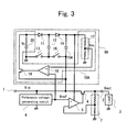
- FIG. 3 is a circuit diagram showing the configuration of a series regulator having an output circuit according to Embodiment 3 of the present invention.
- FIG. 3 components similar to those shown in FIG. 1 are designated by the same numerals, and their descriptions are omitted.
- the configuration shown in FIG. 3 differs from that shown in FIG. 1 in the configuration of the charge pump circuit that is designated by numeral 8 A.
- a DC power supply 10 A for generating the DC voltage Vc comprises a resistor pair 17 that divides the output voltage of the charge pump circuit 8 A, i.e., the bias voltage of the amplifier 5 , and outputs a detection voltage Vsc; an amplifier 18 that amplifies the error between the detection voltage Vsc and the reference voltage Vref generated by the reference voltage generating circuit 6 ; a PMOS transistor 19 , the source terminal of which is connected to the input terminal 1 and the gate terminal of which receives the output of the amplifier 18 so that the PMOS transistor 19 is feedback-controlled; and a capacitor 20 connected between the drain terminal of the PMOS transistor 19 and the ground.
- the configurations of the first rectifying device 11 , the first capacitor 12 , the first switching device 13 and the second rectifying device 14 are the same as those shown in FIG. 1 , and the low-potential terminal of a second capacitor 15 A is connected to the input terminal 1 .
- the DC power supply 10 A of the charge pump circuit 8 A constitutes a series regulator in which the voltage Vc is feedback-controlled so that the output voltage of the charge pump circuit 8 A, serving as the power supply voltage for the amplifier 5 , is stabilized at a predetermined value.
- a voltage Vg is a voltage equal to or higher than the gate-source voltage Vgs that can sufficiently drive the NMOS transistor 4 and is the required minimum voltage
- this predetermined value is set at the voltage (Vout+Vg) obtained by adding the voltage Vg to the output voltage Vout of the series regulator.
- the DC power supply 10 A carries out feedback control so that the voltage Vc of the capacitor 20 to be added to the input voltage Vin becomes (Vout+Vg ⁇ Vin).
- the output voltage of the charge pump circuit 8 A controlled so as to be stabilized at (Vout+Vg) regardless of the input voltage Vin, is supplied to the amplifier 5 as the power supply voltage.
- the power consumption in the amplifier 5 is suppressed to the required minimum as in the embodiments described earlier.
- the rectifying devices of the charge pump circuit are each represented by the symbol of a diode in the drawings.
- the first rectifying device 11 is formed of a switching device that turns on and off in synchronization with the first switching device 13 and the second rectifying device 14 is formed of a switching device that turns on and off in synchronization with the second switching device 16 , for example.
- a series regulator is described in Embodiment 3, even in the case of a power amplifier, a charge pump circuit can also be formed in a way similar to that shown in FIG. 3 as a matter of course.
- a power amplifier is achieved by using a configuration in which the terminal 20 is provided instead of the reference voltage generating circuit 6 and the input signal voltage Vs is input from the outside to the terminal 20 in FIG. 3 .
- an NMOS transistor is used as an output transistor in the embodiments described above, an NPN transistor can also be used.
- Embodiment 1 The difference of Embodiment 1 and Embodiment 2 from Embodiment 3 will herein be described.
- the low-potential side of the output terminals of the charge pump circuit 8 is set at the potential of the other main terminal (the source terminal) of the output transistor 4 .
- the charge pump circuit 8 operates with reference to the output voltage.
- the charge pump circuit 8 A operates with reference to the input voltage.
- the voltage of the capacitor 20 is feedback-controlled so that the power supply voltage of the amplifier 5 (control drive circuit) becomes equal to or higher than the output voltage+the drive threshold voltage.
- the present invention is characterized in that the power supply voltage of the control drive circuit becomes the voltage obtained by adding the voltage equal to or higher than the drive threshold voltage to the output voltage. For this reason, the voltage equal to or higher than the drive threshold voltage can be stably supplied to the control terminal of the output transistor 4 , regardless of the input/output voltages.
- the output circuit of the present invention is useful for series regulators and power amplifiers.
Landscapes
- Engineering & Computer Science (AREA)
- Power Engineering (AREA)
- Continuous-Control Power Sources That Use Transistors (AREA)
- Dc-Dc Converters (AREA)
- Amplifiers (AREA)
Abstract
Description
V8A=Vin+Vc=Vg+Vout
Claims (11)
Applications Claiming Priority (2)
| Application Number | Priority Date | Filing Date | Title |
|---|---|---|---|
| JP2007181743A JP2009020641A (en) | 2007-07-11 | 2007-07-11 | Output circuit |
| JP2007-181743 | 2007-07-11 |
Publications (2)
| Publication Number | Publication Date |
|---|---|
| US20090015299A1 US20090015299A1 (en) | 2009-01-15 |
| US7764113B2 true US7764113B2 (en) | 2010-07-27 |
Family
ID=40252598
Family Applications (1)
| Application Number | Title | Priority Date | Filing Date |
|---|---|---|---|
| US12/169,462 Expired - Fee Related US7764113B2 (en) | 2007-07-11 | 2008-07-08 | Output circuit |
Country Status (2)
| Country | Link |
|---|---|
| US (1) | US7764113B2 (en) |
| JP (1) | JP2009020641A (en) |
Cited By (4)
| Publication number | Priority date | Publication date | Assignee | Title |
|---|---|---|---|---|
| US20100141334A1 (en) * | 2008-12-09 | 2010-06-10 | Pankaj Kumar | Bias circuit scheme for improved reliability in high voltage supply with low voltage device |
| US20120188005A1 (en) * | 2009-07-23 | 2012-07-26 | Reinhard Bachmann | Field Device for Process Instrumentation |
| US8841959B2 (en) * | 2012-03-29 | 2014-09-23 | Hideep Inc. | Circuit and method for removing noise |
| US20140375385A1 (en) * | 2013-06-20 | 2014-12-25 | Fuji Electric Co., Ltd. | Differential amplifier circuit |
Families Citing this family (27)
| Publication number | Priority date | Publication date | Assignee | Title |
|---|---|---|---|---|
| EP2264877B1 (en) * | 2009-06-18 | 2014-04-23 | Alcatel Lucent | Active filter for DC power supply |
| EP2782246B1 (en) | 2010-04-19 | 2018-06-13 | Qorvo US, Inc. | Pseudo-envelope following power management system |
| WO2012047738A1 (en) * | 2010-09-29 | 2012-04-12 | Rf Micro Devices, Inc. | SINGLE μC-BUCKBOOST CONVERTER WITH MULTIPLE REGULATED SUPPLY OUTPUTS |
| US9515621B2 (en) | 2011-11-30 | 2016-12-06 | Qorvo Us, Inc. | Multimode RF amplifier system |
| US9494962B2 (en) | 2011-12-02 | 2016-11-15 | Rf Micro Devices, Inc. | Phase reconfigurable switching power supply |
| US9813036B2 (en) | 2011-12-16 | 2017-11-07 | Qorvo Us, Inc. | Dynamic loadline power amplifier with baseband linearization |
| US8981739B2 (en) * | 2012-09-26 | 2015-03-17 | Nxp B.V. | Low power low dropout linear voltage regulator |
| US9627975B2 (en) | 2012-11-16 | 2017-04-18 | Qorvo Us, Inc. | Modulated power supply system and method with automatic transition between buck and boost modes |
| WO2014116933A2 (en) | 2013-01-24 | 2014-07-31 | Rf Micro Devices, Inc | Communications based adjustments of an envelope tracking power supply |
| US8786324B1 (en) * | 2013-05-13 | 2014-07-22 | Via Technologies, Inc. | Mixed voltage driving circuit |
| EP2997433B1 (en) * | 2013-05-17 | 2020-07-15 | Intel Corporation | On-chip supply generator using dynamic circuit reference |
| US9525337B2 (en) | 2014-04-24 | 2016-12-20 | Qualcomm Incorporated | Charge-recycling circuits |
| US9614476B2 (en) | 2014-07-01 | 2017-04-04 | Qorvo Us, Inc. | Group delay calibration of RF envelope tracking |
| JP6017593B2 (en) | 2015-01-13 | 2016-11-02 | 力晶科技股▲ふん▼有限公司 | Negative reference voltage generation system and manufacturing method thereof |
| US9912297B2 (en) | 2015-07-01 | 2018-03-06 | Qorvo Us, Inc. | Envelope tracking power converter circuitry |
| US9843294B2 (en) | 2015-07-01 | 2017-12-12 | Qorvo Us, Inc. | Dual-mode envelope tracking power converter circuitry |
| US9973147B2 (en) | 2016-05-10 | 2018-05-15 | Qorvo Us, Inc. | Envelope tracking power management circuit |
| US10663993B2 (en) * | 2016-07-15 | 2020-05-26 | Qualcomm Incorporated | Low-dropout regulator with band-reject power supply rejection ratio for phase locked loop voltage controlled oscillator |
| JP6842271B2 (en) * | 2016-10-07 | 2021-03-17 | ラピスセミコンダクタ株式会社 | Power supply circuit and semiconductor storage device |
| US10476437B2 (en) | 2018-03-15 | 2019-11-12 | Qorvo Us, Inc. | Multimode voltage tracker circuit |
| TWI704438B (en) * | 2018-07-12 | 2020-09-11 | 立積電子股份有限公司 | Voltage control device |
| EP3821523B1 (en) * | 2018-10-12 | 2023-06-14 | Yangtze Memory Technologies Co., Ltd. | Ldo regulator using nmos transistor |
| EP3913782A4 (en) | 2019-01-16 | 2022-03-16 | Panasonic Intellectual Property Management Co., Ltd. | DC-DC CONVERTER |
| JP2021141735A (en) * | 2020-03-06 | 2021-09-16 | ファナック株式会社 | Floating power supply circuit |
| US12216485B2 (en) * | 2021-07-08 | 2025-02-04 | Novatek Microelectronics Corp. | Output circuit and related control method with pumping compensation |
| US12147257B2 (en) * | 2022-10-20 | 2024-11-19 | Innolux Corporation | Electronic device with voltage regulator for regulating adjustable level of electronic element |
| CN116149411B (en) * | 2022-11-28 | 2025-08-15 | 圣邦微电子(北京)股份有限公司 | Low dropout linear voltage regulator circuit |
Citations (7)
| Publication number | Priority date | Publication date | Assignee | Title |
|---|---|---|---|---|
| JPH03204013A (en) | 1989-12-29 | 1991-09-05 | Shindengen Electric Mfg Co Ltd | Dropper type constant voltage circuit |
| JPH03204012A (en) | 1989-12-29 | 1991-09-05 | Shindengen Electric Mfg Co Ltd | Dropper type constant voltage circuit |
| JPH04172963A (en) | 1990-11-02 | 1992-06-19 | Nec Corp | Output circuit |
| US5828245A (en) | 1996-10-24 | 1998-10-27 | Stmicroelectronics, Inc. | Driver circuit including amplifier operated in a switching mode |
| US6020781A (en) | 1996-12-27 | 2000-02-01 | Fujitsu Limited | Step-up circuit using two frequencies |
| US6150873A (en) | 1998-06-08 | 2000-11-21 | Samsung Electronics, Co., Ltd. | Internal voltage converter for low operating voltage semiconductor memory |
| US20070222502A1 (en) * | 2006-03-14 | 2007-09-27 | Ippei Noda | Semiconductor apparatus |
-
2007
- 2007-07-11 JP JP2007181743A patent/JP2009020641A/en not_active Withdrawn
-
2008
- 2008-07-08 US US12/169,462 patent/US7764113B2/en not_active Expired - Fee Related
Patent Citations (7)
| Publication number | Priority date | Publication date | Assignee | Title |
|---|---|---|---|---|
| JPH03204013A (en) | 1989-12-29 | 1991-09-05 | Shindengen Electric Mfg Co Ltd | Dropper type constant voltage circuit |
| JPH03204012A (en) | 1989-12-29 | 1991-09-05 | Shindengen Electric Mfg Co Ltd | Dropper type constant voltage circuit |
| JPH04172963A (en) | 1990-11-02 | 1992-06-19 | Nec Corp | Output circuit |
| US5828245A (en) | 1996-10-24 | 1998-10-27 | Stmicroelectronics, Inc. | Driver circuit including amplifier operated in a switching mode |
| US6020781A (en) | 1996-12-27 | 2000-02-01 | Fujitsu Limited | Step-up circuit using two frequencies |
| US6150873A (en) | 1998-06-08 | 2000-11-21 | Samsung Electronics, Co., Ltd. | Internal voltage converter for low operating voltage semiconductor memory |
| US20070222502A1 (en) * | 2006-03-14 | 2007-09-27 | Ippei Noda | Semiconductor apparatus |
Cited By (7)
| Publication number | Priority date | Publication date | Assignee | Title |
|---|---|---|---|---|
| US20100141334A1 (en) * | 2008-12-09 | 2010-06-10 | Pankaj Kumar | Bias circuit scheme for improved reliability in high voltage supply with low voltage device |
| US7902904B2 (en) * | 2008-12-09 | 2011-03-08 | Lsi Corporation | Bias circuit scheme for improved reliability in high voltage supply with low voltage device |
| US20120188005A1 (en) * | 2009-07-23 | 2012-07-26 | Reinhard Bachmann | Field Device for Process Instrumentation |
| US8593214B2 (en) * | 2009-07-23 | 2013-11-26 | Siemens Aktiengesellschaft | Field device for process instrumentation |
| US8841959B2 (en) * | 2012-03-29 | 2014-09-23 | Hideep Inc. | Circuit and method for removing noise |
| US20140375385A1 (en) * | 2013-06-20 | 2014-12-25 | Fuji Electric Co., Ltd. | Differential amplifier circuit |
| US9484873B2 (en) * | 2013-06-20 | 2016-11-01 | Fuji Electric Co., Ltd. | Differential amplifier circuit |
Also Published As
| Publication number | Publication date |
|---|---|
| JP2009020641A (en) | 2009-01-29 |
| US20090015299A1 (en) | 2009-01-15 |
Similar Documents
| Publication | Publication Date | Title |
|---|---|---|
| US7764113B2 (en) | Output circuit | |
| JP4744945B2 (en) | Regulator circuit | |
| US10452087B2 (en) | Low drop-out regulator | |
| US7932707B2 (en) | Voltage regulator with improved transient response | |
| US8148962B2 (en) | Transient load voltage regulator | |
| US20140084896A1 (en) | Low power low dropout linear voltage regulator | |
| US7928708B2 (en) | Constant-voltage power circuit | |
| US20110050198A1 (en) | Low-power voltage regulator | |
| US12287659B2 (en) | Low-dropout regulator for low voltage applications | |
| JP5444869B2 (en) | Output device | |
| JP4833651B2 (en) | Regulator circuit and automobile equipped with the same | |
| US8085018B2 (en) | Voltage regulator with phase compensation | |
| US7135912B2 (en) | Methods and systems for decoupling the stabilization of two loops | |
| US9817427B2 (en) | Static offset reduction in a current conveyor | |
| US9075423B2 (en) | Generating a regulated signal from another regulated signal | |
| KR102317348B1 (en) | Low Drop Out Voltage Regulator Using Dual Push-Pull Circuit | |
| JP2017126259A (en) | Power supply | |
| JP2014128038A (en) | Power supply device | |
| US11442480B2 (en) | Power supply circuit alternately switching between normal operation and sleep operation | |
| US11592854B2 (en) | Linear voltage regulator | |
| US7352163B2 (en) | Early effect cancelling circuit, differential amplifier, linear regulator, and early effect canceling method | |
| US10969810B2 (en) | Voltage regulator with virtual zero quiescent current | |
| JP4211369B2 (en) | AGC circuit | |
| KR20240053781A (en) | Low drop out regulator | |
| JPH11134044A (en) | Constant voltage power supply circuit |
Legal Events
| Date | Code | Title | Description |
|---|---|---|---|
| AS | Assignment |
Owner name: MATSUSHITA ELECTRIC INDUSTRIAL CO., LTD., JAPAN Free format text: ASSIGNMENT OF ASSIGNORS INTEREST;ASSIGNORS:RYU, TAKASHI;ISHII, TAKUYA;NAKAMURA, NAOYUKI;AND OTHERS;REEL/FRAME:021292/0247;SIGNING DATES FROM 20080620 TO 20080627 Owner name: MATSUSHITA ELECTRIC INDUSTRIAL CO., LTD., JAPAN Free format text: ASSIGNMENT OF ASSIGNORS INTEREST;ASSIGNORS:RYU, TAKASHI;ISHII, TAKUYA;NAKAMURA, NAOYUKI;AND OTHERS;SIGNING DATES FROM 20080620 TO 20080627;REEL/FRAME:021292/0247 |
|
| AS | Assignment |
Owner name: PANASONIC CORPORATION, JAPAN Free format text: CHANGE OF NAME;ASSIGNOR:MATSUSHITA ELECTRIC INDUSTRIAL CO., LTD.;REEL/FRAME:021897/0624 Effective date: 20081001 Owner name: PANASONIC CORPORATION,JAPAN Free format text: CHANGE OF NAME;ASSIGNOR:MATSUSHITA ELECTRIC INDUSTRIAL CO., LTD.;REEL/FRAME:021897/0624 Effective date: 20081001 |
|
| STCF | Information on status: patent grant |
Free format text: PATENTED CASE |
|
| FEPP | Fee payment procedure |
Free format text: PAYOR NUMBER ASSIGNED (ORIGINAL EVENT CODE: ASPN); ENTITY STATUS OF PATENT OWNER: LARGE ENTITY |
|
| FPAY | Fee payment |
Year of fee payment: 4 |
|
| MAFP | Maintenance fee payment |
Free format text: PAYMENT OF MAINTENANCE FEE, 8TH YEAR, LARGE ENTITY (ORIGINAL EVENT CODE: M1552) Year of fee payment: 8 |
|
| AS | Assignment |
Owner name: PANASONIC SEMICONDUCTOR SOLUTIONS CO., LTD., JAPAN Free format text: ASSIGNMENT OF ASSIGNORS INTEREST;ASSIGNOR:PANASONIC CORPORATION;REEL/FRAME:052755/0917 Effective date: 20200521 |
|
| FEPP | Fee payment procedure |
Free format text: MAINTENANCE FEE REMINDER MAILED (ORIGINAL EVENT CODE: REM.); ENTITY STATUS OF PATENT OWNER: LARGE ENTITY |
|
| LAPS | Lapse for failure to pay maintenance fees |
Free format text: PATENT EXPIRED FOR FAILURE TO PAY MAINTENANCE FEES (ORIGINAL EVENT CODE: EXP.); ENTITY STATUS OF PATENT OWNER: LARGE ENTITY |
|
| STCH | Information on status: patent discontinuation |
Free format text: PATENT EXPIRED DUE TO NONPAYMENT OF MAINTENANCE FEES UNDER 37 CFR 1.362 |
|
| FP | Lapsed due to failure to pay maintenance fee |
Effective date: 20220727 |