US7759696B2 - High-breakdown voltage semiconductor switching device and switched mode power supply apparatus using the same - Google Patents
High-breakdown voltage semiconductor switching device and switched mode power supply apparatus using the same Download PDFInfo
- Publication number
- US7759696B2 US7759696B2 US11/582,441 US58244106A US7759696B2 US 7759696 B2 US7759696 B2 US 7759696B2 US 58244106 A US58244106 A US 58244106A US 7759696 B2 US7759696 B2 US 7759696B2
- Authority
- US
- United States
- Prior art keywords
- region
- collector
- drain
- resurf
- switching device
- Prior art date
- Legal status (The legal status is an assumption and is not a legal conclusion. Google has not performed a legal analysis and makes no representation as to the accuracy of the status listed.)
- Active, expires
Links
Images


Classifications
-
- H—ELECTRICITY
- H10—SEMICONDUCTOR DEVICES; ELECTRIC SOLID-STATE DEVICES NOT OTHERWISE PROVIDED FOR
- H10D—INORGANIC ELECTRIC SEMICONDUCTOR DEVICES
- H10D12/00—Bipolar devices controlled by the field effect, e.g. insulated-gate bipolar transistors [IGBT]
- H10D12/411—Insulated-gate bipolar transistors [IGBT]
-
- H—ELECTRICITY
- H10—SEMICONDUCTOR DEVICES; ELECTRIC SOLID-STATE DEVICES NOT OTHERWISE PROVIDED FOR
- H10D—INORGANIC ELECTRIC SEMICONDUCTOR DEVICES
- H10D62/00—Semiconductor bodies, or regions thereof, of devices having potential barriers
- H10D62/10—Shapes, relative sizes or dispositions of the regions of the semiconductor bodies; Shapes of the semiconductor bodies
- H10D62/102—Constructional design considerations for preventing surface leakage or controlling electric field concentration
- H10D62/103—Constructional design considerations for preventing surface leakage or controlling electric field concentration for increasing or controlling the breakdown voltage of reverse-biased devices
- H10D62/105—Constructional design considerations for preventing surface leakage or controlling electric field concentration for increasing or controlling the breakdown voltage of reverse-biased devices by having particular doping profiles, shapes or arrangements of PN junctions; by having supplementary regions, e.g. junction termination extension [JTE]
- H10D62/109—Reduced surface field [RESURF] PN junction structures
Definitions
- the present invention relates to a switched mode power supply apparatus, and more particularly, it relates to a high-breakdown voltage semiconductor switching device used in a switched mode power supply apparatus for repeatedly switching a principal current.
- FIG. 22 shows an exemplified circuit configuration of the conventional switched mode power supply apparatus.
- the conventional switched mode power supply apparatus includes a primary rectifying/smoothing circuit 111 , a main circuit 112 , a transformer 104 and a secondary rectifying/smoothing circuit 121 .
- an AC voltage input between input terminals 116 and 117 of the primary rectifying/smoothing circuit 111 is rectified and smoothed by the primary rectifying/smoothing circuit 111 so as to be supplied to the main circuit 112 as an input DC voltage.
- the primary rectifying/smoothing circuit 111 includes a diode bridge 131 and an input capacitor 132 , so that a voltage having been full-wave rectified by the diode bridge 131 can be smoothed by the input capacitor 132 for supplying the resultant voltage to the main circuit 112 .
- the main circuit 112 includes a semiconductor switching device 113 and a voltage control circuit 114 .
- the semiconductor switching device 113 and the voltage control circuit 114 can be integrated on one chip.
- the transformer 104 includes a primary winding 141 , and the primary winding 141 and the semiconductor switching device 113 are serially connected to each other, and the input DC voltage is supplied from the primary rectifying/smoothing circuit 111 to this serially connected circuit.
- the control terminal of the semiconductor switching device 113 is connected to the voltage control circuit 114 , so that the semiconductor switching device 113 can be controlled to be turned on/off in accordance with a gate signal output by the voltage control circuit 114 .
- the transformer 104 further includes a secondary winding 142 magnetically coupled to the primary winding 141 and a bias winding 143 magnetically coupled to the primary winding 141 and the secondary winding 142 .
- the second rectifying/smoothing circuit 121 generates a DC output voltage by rectifying and smoothing the voltage induced in the secondary winding 142 and outputs the DC output voltage from output terminals 126 and 127 .
- the secondary rectifying/smoothing circuit 121 includes a diode 122 , a choke coil 123 and first and second output capacitors 124 and 125 .
- the choke coil 123 and the first and second output capacitors 124 and 125 are connected to one another in a ⁇ shape, and the voltage induced in the secondary winding 142 is half-wave rectified by the diode 122 and is smoothed by the choke coil 123 and the first and second output capacitors 124 and 125 .
- a voltage generated on the both ends of the bias winding 143 is input to the control terminal of the semiconductor switching device 113 through the voltage control circuit 114 .
- the switched mode power supply apparatus of FIG. 22 employs a ringing choke converter (RCC) system, and the semiconductor switching device 113 performs a switching operation in a self-excited manner by using the voltage generated in the bias winding 143 .
- RRC ringing choke converter
- a voltage between the output terminals 126 and 127 is fed back to the voltage control circuit 114 through a photo coupler 129 .
- the voltage control circuit 114 forcedly increases an on period of the semiconductor switching device 113 , and on the contrary, in the case where the voltage between the output terminals 126 and 127 is increased, the voltage control circuit 114 forcedly reduces an on period of the semiconductor switching device 113 .
- the voltage appearing between the output terminals 126 and 127 is kept at a given value.
- an auxiliary DC voltage is generated by using the voltage induced in the bias winding 143 , and therefore, the voltage control circuit 114 is operated by the auxiliary DC voltage except for the starting time of the switched mode power supply apparatus.
- the semiconductor switching device 113 In the starting time of the switched mode power supply apparatus, namely, when the AC voltage is applied between the input terminals 116 and 117 , the semiconductor switching device 113 is not in a switching operation, and hence, no voltage is induced in the bias winding 143 and no power is supplied to the voltage control circuit 114 . Accordingly, in order to start the switching operation of the semiconductor switching device 113 , a low voltage sufficient for activating the voltage control circuit 114 is supplied from the primary rectifying/smoothing circuit 111 through an externally provided resistance 151 (with a high breakdown voltage and high power).
- loss is mainly caused in the semiconductor switching device 113 .
- a MOSFET metal oxide semiconductor field effect transistor
- switching loss caused in turn off is large in a bipolar transistor but the switching loss is small in a MOSFET because its switching speed is high.
- a MOSFET has large conducting resistance differently from a bipolar transistor and hence its conducting loss cannot be ignored. Accordingly, when a large current passes through a MOSFET, large loss is caused.
- bipolar type IGBT insulated gate bipolar transistor
- the switching frequency of the switching device 113 is lowered and an on period of the switching device 113 is increased, and as a result, a large current passes through the primary winding 141 so as to keep the voltage between the output terminals 126 and 127 at a given value.
- the switching frequency of the switching device 113 is increased and an on period is reduced, and as a result, the current passing through the primary winding 141 is reduced so as to keep the voltage between the output terminals 126 and 127 at a given value.
- FIG. 23 is a diagram for showing the comparison, in the relationship between load and loss, between a MOSFET (of a lateral type having a drift region with a resurf structure) and an IGBT (of a lateral type) used in a switched mode power supply apparatus.
- a MOSFET of a lateral type having a drift region with a resurf structure
- an IGBT of a lateral type
- Patent Document 1 Japanese Laid-Open Patent Publication No. 7-153951
- Patent Document 2 Japanese Laid-Open Patent Publication No. 2002-345242
- Patent Document 3 Japanese Patent Publication No. 6-52791 (U.S. Pat. No. 5,072,268)
- Non-patent Document 1 D. S. Byeon et al., The separated shorted-anode insulated gate bipolar transistor with the suppressed negative differential resistance regime, Microelectronics Journal 30, 1999, pp. 571-575
- the conducting loss is large when the load is heavy, and in the case where an IGBT is used as the switching device, the switching loss is large in the standby mode or when the load is light. Accordingly, it is difficult to reduce the loss in the whole region ranging from light load to heavy load in a conventional semiconductor switching device.
- an object of the invention is providing a high-breakdown voltage semiconductor switching device whose loss can be reduced in the whole region ranging from light load to heavy load and a switched mode power supply apparatus using the same.
- the present inventors have examined proper use of two kinds of transistors, namely, a MOSFET and an IGBT, in one switched mode power supply apparatus.
- Patent Document 1 proposes an architecture where a vertical IGBT and a vertical power MOSFET are both provided in one chip of a switching device.
- the current power of the vertical power MOSFET is too small as compared with the driving power of the vertical IGBT, and as a result, it is practically difficult to drive the power MOSFET when the load is light.
- a step should be formed on the back face of a semiconductor substrate, and hence, the fabrication process is difficult.
- Patent Document 2 proposes an architecture where an IGBT of a Schottky junction type is used as the switching device.
- the loss caused when the load is light is larger than that of a power MOSFET, and the loss caused when the load is heavy is larger than that of a conventional IGBT. Therefore, this architecture of Patent Document 2 cannot always reduce the loss.
- the switching device described in any of Patent Documents 1 and 2 has a vertical structure. Therefore, when such a vertical switching device is used as the semiconductor switching device 113 of, for example, the conventional switched mode power supply apparatus of FIG. 22 , there arises another problem that it is difficult to build the voltage control circuit 114 and the semiconductor switching device 113 in one chip.
- Patent Document 3 and Non-patent Document 1 propose shorted-anode lateral IGBTs serving as an intermediate between the MOSFET and the IGBT, though their object is not to achieve the use of two kinds of a MOSFET and an IGBT in one element.
- FIG. 24 is a cross-sectional view for showing one example of a shorted-anode lateral IGBT disclosed in Patent Document 3.
- a P + -type pocket 514 and an N + -type pocket 515 are shorted through a drain electrode 513 .
- the current starts flowing from the N + -pocket 515 to a source electrode 505 via an N + -type source region 507 (MOSFET operation).
- the present inventors have reached the invention of a lateral high-breakdown semiconductor switching element described below. Namely, the invention achieves a switching element which is capable of switching between a MOSFET and an IGBT by a single element, which reduces the loss in the whole region ranging from light load to heavy load, and which can be built in one chip together with a control circuit and the like.
- the first high-breakdown voltage semiconductor switching device of this invention includes a resurf region of a second conductivity type formed in a surface portion of a semiconductor substrate of a first conductivity type; a base region of the first conductivity type formed in the semiconductor substrate to be adjacent to the resurf region; an emitter/source region of the second conductivity type formed in the base region to be spaced from the resurf region; a gate insulating film formed over the base region to cover a portion of the emitter/source region and a portion of the resurf region; a gate electrode formed on the gate insulating film; a drain region of the second conductivity type formed in the resurf region to be spaced from the base region; a collector region of the first conductivity type formed in the resurf region to be spaced from the base region; a collector/drain electrode formed on the semiconductor substrate and electrically connected to the collector region and the drain region; and an emitter/source electrode formed on the semiconductor substrate and electrically connected to the base region and the
- a MOSFET operation can be performed when a collector current passing through the device is comparatively small and an IGBT operation can be performed when the collector current becomes large.
- two kinds of transistors that is, a MOSFET and an IGBT, can be properly used in one device. Accordingly, the MOSFET operation can be performed in a standby mode or when load is light and the IGBT operation can be performed when the load is heavy, so that loss can be reduced in a whole region ranging from light load to heavy load in the high-breakdown voltage semiconductor switching device.
- an extended drain region that corresponds to, for example, an N-type resurf region 202 of Embodiment 1 described below and is a region for principally keeping a breakdown voltage
- an extended drain region that corresponds to, for example, an N-type resurf region 202 of Embodiment 1 described below and is a region for principally keeping a breakdown voltage
- the resistance obtained in the MOSFET operation can be lowered by the resurf layer with a high impurity concentration. Therefore, as compared with a conventional lateral device, a large collector (drain) current can be allowed to pass in the MOSFET operation.
- the first high-breakdown voltage semiconductor switching device of this invention is a lateral device in which a collector electrode (collector/drain electrode) and an emitter electrode (emitter/source electrode) are provided on the same principal face of a substrate, it can be built on one chip together with a gate signal control circuit or the like.
- each of the collector region and the drain region preferably includes a plurality of sections separated from one another, and the sections of the collector region and the sections of the drain region are preferably alternately arranged to be in contact with one another along a vertical direction to a direction extending from the collector region toward the emitter/source region.
- change in length of each section of the collector region allows the MOSFET operation to be changed to the IGBT operation easily without inviting an increase in element area as compared with the case where the respective sections of the collector region and the respective sections of the drain region are arranged, for example, along the direction extending from the collector region toward the emitter/source region.
- each section of the collector region has a length of 48 ⁇ m or less along the vertical direction to the direction extending from the collector region toward the emitter/source region, a fall time tf can be shortened as compared with the case where the length of each section of the collector region is larger than 48 ⁇ m, and hence, switching loss can be thus reduced. Also, as compared with the case where the length of each section of the collector region is larger than 48 ⁇ m, the collector voltage Vch at which the MOSFET operation is changed to the IGBT operation can be increased, and hence, a more practical light-loaded MOSFET operation can be performed.
- arrangement of the sections of the collector region and the sections of the drain region is preferably terminated by a terminating portion corresponding to a part of the drain region
- a second drain region of the second conductivity type is preferably formed in the resurf region to be spaced from the base region
- a second drain electrode electrically connected to the second drain region is preferably formed on the semiconductor substrate
- the second drain region is preferably electrically connected to the terminating portion of the drain region through the resurf region
- at least a part of a portion of the resurf region disposed between the second drain region and the terminating portion of the drain region preferably has a smaller width than other portions, whereby pinching off a current path from the terminating portion of the drain region to the second drain region through an electric field effect when a voltage exceeding a given value is applied to the collector/drain electrode.
- the collector electrode collector/drain electrode
- a voltage appearing on the second drain electrode can be pinched off (lowered) by a depletion layer expanding from the semiconductor substrate to the resurf region. Accordingly, when the voltage of the second drain electrode is pinched off, for example, to approximately 10 V, the second drain electrode can be connected to a device of a low voltage circuit for supplying power to the device.
- a buffer layer of the second conductivity type having a higher impurity concentration than the resurf region is preferably provided between the collector region and the resurf region.
- the efficiency for injecting holes from the collector region into the resurf region is reduced, and hence, for example, the fall time tf can be improved to be shorter.
- one or a plurality of semiconductor layers of the first conductivity type electrically connected to the base region are preferably formed in the resurf region.
- the impurity concentration of the resurf region can be increased, and hence, the conducting resistance obtained in the MOSFET operation is reduced.
- the collector (drain) current passing in the MOSFET operation can be further increased, so that a more practical light-loaded MOSFET operation can be performed.
- the fall time tf can be shortened.
- the impurity concentration of the resurf region can be increased, the life time of holes in the resurf region can be shortened, so as to shorten the fall time tf.
- the switched mode power supply apparatus of this invention includes a semiconductor switching device to which an input DC voltage is applied; a voltage control circuit for controlling switching of the semiconductor switching device; a primary winding electrically connected to an output terminal of the semiconductor switching device; a secondary winding magnetically coupled to the primary winding; and a rectifying/smoothing circuit for rectifying and smoothing a voltage induced in the secondary winding for supplying an output DC voltage to a load, and the semiconductor switching device is the first high-breakdown voltage semiconductor switching device of the invention.
- the switched mode power supply apparatus of this invention uses the first high-breakdown voltage semiconductor switching device of this invention, switching loss can be reduced by performing the MOSFET operation when load is light and conducting loss can be reduced by performing the IGBT operation when the load is heavy. Accordingly, the loss can be reduced in the whole region ranging from light load to heavy load in the switched mode power supply apparatus.
- each of the collector region and the drain region preferably includes a plurality of sections separated from one another, and the sections of the collector region and the sections of the drain region are preferably alternately arranged to be in contact with one another along a vertical direction to a direction extending from the collector region toward the emitter/source region.
- arrangement of the sections of the collector region and the sections of the drain region is preferably terminated by a terminating portion corresponding to a part of the drain region, a second drain region of the second conductivity type is preferably formed in the resurf region to be spaced from the base region, a second drain region electrically connected to the second drain region is preferably formed on the semiconductor substrate, the second drain region is preferably electrically connected to the terminating portion of the drain region through the resurf region, and at least a part of a portion of the resurf region disposed between the second drain region and the terminating portion of the drain region preferably has a smaller width than other portions, whereby pinching off a current path from the terminating portion of the drain region to the second drain region through an electric field effect when a voltage exceeding a given value is applied to the collector/drain electrode.
- the switched mode power supply apparatus of this invention preferably further includes a starting circuit for starting the voltage control circuit, and the second drain electrode of the
- a low bias starting voltage necessary in power supply can be generated within the high-breakdown voltage semiconductor switching device, and therefore, a power supply apparatus can be constructed without using a high-breakdown voltage and high-power resistance for power supply that is conventionally necessary.
- the switched mode power supply apparatus of the invention preferably further includes a bias winding magnetically coupled to the primary winding and the secondary winding, and the switched mode power supply apparatus preferably employs a ringing choke converter system in which a voltage induced in the bias winding is applied to a gate terminal of the semiconductor switching device through the voltage control circuit.
- the switching frequency is increased when the load is light and is reduced when the load is heavy, and therefore, the first high-breakdown voltage semiconductor switching device of this invention that performs the MOSFET operation when the load is light and performs the IGBT operation when the load is heavy can be more effectively used.
- the second high-breakdown voltage semiconductor switching device of this invention includes a resurf region of a second conductivity type formed in a surface portion of a semiconductor substrate of a first conductivity type; a base region of the first conductivity type formed in the semiconductor substrate to be adjacent to the resurf region; an emitter/source region of the second conductivity type formed in the base region to be spaced from the resurf region; a gate insulating film formed over the base region to cover a portion of the emitter/source region and a portion of the resurf region; a gate electrode formed on the gate insulating film; a drain region of the second conductivity type formed in the resurf region to be spaced from the base region; a first collector region of the first conductivity type formed in the resurf region to be spaced from the base region; a second collector region of the first conductivity type formed in the resurf region to be spaced from the base region; a collector/drain electrode formed on the semiconductor substrate and electrically connected to the first collector
- the voltage Vch can be determined in accordance with the length X 1 of each section of the first collector region larger than the length X 2 of each section of the second collector region. Also, owing to the second collector region including the sections each having the length X 2 smaller than the length X 1 of each section of the first collector region, the total area of the whole collector region can be suppressed, so as to shorten the fall time tf caused in turn off. Accordingly, both of the voltage Vch and the fall time tf can be suppressed, so as to improve a trade-off relationship between the voltage Vch and the fall time tf.
- the number of sections of the first collector region is preferably smaller than the number of sections of the second collector region.
- the total area of the whole collector region can be further suppressed, so as to further shorten the fall time tf caused in turn off.
- the first collector region is preferably composed of a third collector region including a plurality of sections each having a given length Z along the vertical direction and a fourth collector region including a plurality of sections each having a given length X 1 -Z along the vertical direction, and a portion of the resurf region not connected to the collector/drain electrode is preferably sandwiched between and in contact with a section of the third collector region and a section of the fourth collector region along the vertical direction.
- a wiring made of, for example, polysilicon can be formed above the portion of the resurf region.
- the design freedom for the circuit pattern can be improved without degrading the device performance.
- the collector/drain electrode is preferably drawn onto an interlayer film formed above the resurf region
- the high-breakdown voltage semiconductor switching device preferably further includes a drain electric field reducing layer formed between the interlayer film and the resurf region and electrically connected to the collector/drain electrode, and at least a part of the drain electric field reducing layer is preferably disposed below a portion of the collector/drain electrode drawn onto the interlayer film and disposed above the portion of the resurf region sandwiched between a section of the third collector region and a section of the fourth collector region.
- the drain electric field reducing layer is preferably connected to the collector/drain electrode above the portion of the resurf region sandwiched between a section of the third collector region and a section of the fourth collector region.
- the present invention relates a high-breakdown voltage semiconductor switching device and a switched mode power supply apparatus using the same and is very useful because it attains a special effect to reduce loss in the whole region ranging from light load to heavy load.
- FIG. 1 is a cross-sectional view of a high-breakdown voltage semiconductor switching device according to Embodiment 1 of the invention
- FIG. 2 is a plan view of the high-breakdown voltage semiconductor switching device according to Embodiment 1 of the invention.
- FIG. 3 is another cross-sectional view of the high-breakdown voltage semiconductor switching device according to Embodiment 1 of the invention.
- FIG. 4 is a plan view of a JFET portion of the high-breakdown voltage semiconductor switching device of Embodiment 1;
- FIG. 5 is a cross-sectional view of the JFET portion of the high-breakdown voltage semiconductor switching device of Embodiment 1;
- FIG. 6 is a diagram for showing the correlation between a collector voltage and a collector current in the high-breakdown voltage semiconductor switching device of Embodiment 1;
- FIG. 7 is a diagram for showing the correlation among a collector region length X, a fall time tf and a collector voltage Vch for changing to an IGBT operation in the high-breakdown voltage semiconductor switching device of Embodiment 1;
- FIG. 8 is a diagram for showing an exemplified circuit configuration of a switched mode power supply apparatus according to Embodiment 1 of the invention.
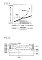
- FIG. 9 is a diagram for showing the relationship between load and loss obtained when the high-breakdown voltage semiconductor switching device of Embodiment 1 is used in the switched mode power supply apparatus;
- FIG. 10 is a cross-sectional view of a high-breakdown voltage semiconductor switching device according to Embodiment 2 of the invention.
- FIG. 11 is a cross-sectional view of a high-breakdown voltage semiconductor switching device according to Embodiment 3 of the invention.
- FIG. 12 is a plan view of a high-breakdown voltage semiconductor switching device according to Embodiment 4 of the invention.
- FIG. 13 is a plan view of a high-breakdown voltage semiconductor switching device according to Embodiment 5 of the invention.
- FIGS. 14A , 14 B and 14 C are cross-sectional views of the high-breakdown voltage semiconductor switching device according to Embodiment 5 of the invention.
- FIG. 15 is a diagram for showing the correlation between a collector voltage Vch for changing to an IGBT operation and a fall time tf in the high-breakdown voltage semiconductor switching device of Embodiment 5;
- FIG. 16 is a schematic diagram for showing comparison between a collector/drain region structure of the high-breakdown voltage semiconductor switching device of Embodiment 5 and other collector/drain region structures;
- FIG. 17 is a table of measured characteristics of the high-breakdown voltage semiconductor switching device of Embodiment 5 compared with measured characteristics of another high-breakdown voltage semiconductor switching device;
- FIG. 18 is a plan view of a high-breakdown voltage semiconductor switching device according to Embodiment 6 of the invention.
- FIGS. 19A , 19 B and 19 C are cross-sectional views of the high-breakdown voltage semiconductor switching device of Embodiment 6;
- FIG. 20 is a plan view of a high-breakdown voltage semiconductor switching device according to Embodiment 7 of the invention.
- FIGS. 21A , 21 B, 21 C, 21 D and 21 E are cross-sectional views of the high-breakdown voltage semiconductor switching device of Embodiment 7;
- FIG. 22 is a diagram for showing an exemplified circuit configuration of a conventional switched mode power supply apparatus.
- FIG. 23 is a diagram for showing the comparison, in the relationship between load and loss, between a MOSFET (of a lateral type having a drift region with a resurf structure) and an IGBT (of a lateral type) used in a switched mode power supply apparatus.
- FIG. 24 is a cross-sectional view for showing one example of a conventional shorted-anode lateral IGBT.
- FIGS. 1 through 3 are diagrams for showing an exemplified architecture of the high-breakdown voltage semiconductor switching device of this embodiment, and specifically, FIG. 2 is a plan view thereof, FIG. 1 is a cross-sectional view thereof taken on line A-A′ of FIG. 2 and FIG. 3 is a cross-sectional view thereof taken on line B-B′ of FIG. 2 . It is noted that part of composing elements is omitted in FIG. 2 .
- an N-type resurf region 202 with a concentration of, for example, approximately 1 ⁇ 10 16 /cm 3 and a depth of approximately 7 ⁇ m is formed in a surface portion of a P ⁇ type semiconductor substrate 201 with a concentration of, for example, approximately 1 ⁇ 10 14 /cm 3 .
- a p-type base region 204 with a concentration of, for example, approximately 1 ⁇ 10 17 /cm 3 is formed in the semiconductor substrate 201 to be adjacent to the resurf region 202 .
- a P + type contact region 205 with a concentration of, for example, approximately 1 ⁇ 10 19 /cm 3 and an N + type emitter/source region 206 with a concentration of, for example, approximately 1 ⁇ 10 20 /cm 3 are formed to be adjacent to each other and spaced from the resurf region 202 .
- the contact region 205 is farther from the resurf region 202 than the emitter/source region 206 .
- a gate insulating film 209 is formed over the base region 204 so as to cover a portion of the emitter/source region 206 and at least an end portion of the resurf region 202 .
- a gate electrode 210 is formed on the gate insulating film 209 .
- a p + type collector region 203 with a concentration of, for example, approximately 1 ⁇ 10 19 /cm 3 is formed in the resurf region 202 to be spaced from the base region 204
- an N + type drain region 213 with a concentration of, for example, approximately 1 ⁇ 10 20 /cm 3 is formed in the resurf region 202 to be spaced from the base region 204 .
- each of the collector region 203 and the drain region 213 includes a plurality of sections separated from one another, and the respective sections of the collector region 203 and the respective sections of the drain region 213 are alternately arranged to be in contact with one another along a vertical direction to a direction extending from the collector region 203 toward the emitter/source region 206 .
- the length X is, for example, approximately 40 ⁇ m
- the length Y is, for example, approximately 10 ⁇ m.
- a collector/drain electrode 211 electrically connected to both of the collector region 203 and the drain region 213 is formed on the semiconductor substrate 201
- an emitter/source electrode 212 electrically connected to both of the base region 204 and the emitter/source region 206 is formed on the semiconductor substrate 201 .
- the emitter/source electrode 212 is electrically connected to the base region 204 through the contact region 205 .
- an interlayer film 208 is formed above the resurf region 202 with a field insulating film 207 sandwiched therebetween, and the collector/drain electrode 211 and the emitter/source electrode 212 are drawn onto the interlayer film 208 .
- a positive bias voltage hereinafter sometimes referred to as a collector voltage
- a positive voltage hereinafter sometimes referred to as a collector current
- a collector current starts to flow from the drain region 213 to the emitter/source electrode 212 through the resurf region 202 , the base region 204 (a portion thereof corresponding to a channel region) and the emitter/source region 206 (which operation is a MOSFET operation).
- FIG. 6 shows the correlation between the collector voltage and the collector current obtained in the high-breakdown voltage semiconductor switching device of this embodiment.
- the voltage Vch can be controlled in accordance with the collector region length X shown in FIG. 2 (i.e., the length of each section of the collector region 203 along the vertical direction to the direction extending from the collector region 203 toward the emitter/source region 206 ).
- the length Y is the drain region length (i.e., the length of each section of the drain region 213 along the vertical direction to the direction extending from the collector region 203 toward the emitter/source region 206 ).
- FIG. 7 shows the correlation among the collector region length X, a fall time tf caused in turn off (i.e., a time required after turn off for the collector current to reduce (change) from 90% of its peak value to 10%) and the voltage Vch obtained in the high-breakdown voltage semiconductor switching device of this embodiment.
- a fall time tf caused in turn off i.e., a time required after turn off for the collector current to reduce (change) from 90% of its peak value to 10%
- the voltage Vch obtained in the high-breakdown voltage semiconductor switching device of this embodiment.
- the collector region length X is shorter, the fall time tf is shorter and the switching loss is smaller. It is noted that the voltage Vch should be approximately 2 V or more for realizing a practical light-loaded MOSFET operation. Accordingly, in the high-breakdown voltage semiconductor switching device of this embodiment, the collector region length X is preferably designed to be 48 ⁇ m or less.
- the high-breakdown voltage semiconductor switching device of this embodiment can be made to perform the MOSFET operation when the collector current passing therethrough is comparatively small and to perform the IGBT operation when the collector current is large. Therefore, two kinds of transistors, namely, the MOSFET and the IGBT, can be properly used in one device. Accordingly, the MOSFET operation can be performed in a standby mode or when load is light and the IGBT operation can be performed when the load is heavy. Thus, a high-breakdown voltage semiconductor switching device whose loss can be reduced in the whole region ranging from light load to heavy load can be realized.
- the high-breakdown voltage semiconductor switching device of this embodiment uses the N-type resurf region 202 , the conducting resistance obtained in the MOSFET operation can be lowered by the resurf region 202 with a high impurity concentration. Therefore, as shown in FIG. 6 , a larger collector (drain) current can be allowed to pass in the MOSFET operation than in a conventional lateral device.
- each of the collector region 203 and the drain region 213 includes a plurality of separated sections, and the respective sections of the collector region 203 and the respective sections of the drain region 213 are alternately arranged to be in contact with one another along the vertical direction to the direction extending from the collector region 203 toward the emitter/source region 206 . Accordingly, the MOSFET operation is changed to the IGBT operation easily without inviting an increase in element area.
- the MOSFET operation is hardly changed to the IGBT operation unless the length of the collector region 203 in the direction extending toward the emitter/source region 206 is made large.
- the MOSFET operation is performed in the load range where the IGBT operation is preferable primarily, thereby increasing the loss.
- the length X of the collector region 203 is changed, enabling easy change from the MOSFET operation to the IGBT operation without inviting an increase in element area.
- the high-breakdown voltage semiconductor switching device of this embodiment is a lateral device in which the collector/drain electrode 211 and the emitter/source electrode 212 are provided on the same principal face of the semiconductor substrate 201 , it can be built on one chip together with a gate signal control circuit or the like.
- each of the collector region 203 and the drain region 213 includes a plurality of separated sections and the respective sections of the collector region 203 and the respective sections of the drain region 213 are alternately disposed to be in contact with one another along the vertical direction to the direction extending from the collector region 203 toward the emitter/source region 206 .
- both or one of the collector region 203 and the drain region 213 may be formed as a single region.
- the arrangement of the sections of the collector region 203 and the drain region 213 is not particularly specified excluding the arrangement in which the MOSFET operation can be easily changed to the IGBT operation as described above.
- FIG. 4 is a plan view of the high-breakdown voltage semiconductor switching device of this embodiment for showing a region not shown in the plan view of FIG. 2
- FIG. 5 is a cross-sectional view thereof taken on line C-C′ of FIG. 4 .
- the arrangement of the respective sections of the collector region 203 and the respective sections of the drain region 213 is terminated by an N + type drain region (terminating drain region) 218 with a concentration of, for example, approximately 1 ⁇ 10 20 /cm 3 corresponding to a part of the drain region 213 .
- an N + type second drain region 219 with a concentration of, for example, approximately 1 ⁇ 10 20 /cm 3 is formed in the resurf region 202 to be spaced from the base region 204 .
- a second drain electrode 220 electrically connected to the second drain region 219 is formed on the semiconductor substrate 201 .
- the second drain electrode 220 is drawn onto the interlayer film 208 .
- the second drain region 219 and the terminating drain region 218 are electrically connected to each other through the resurf region 202 .
- a portion 51 of the resurf region 202 disposed between the second drain region 219 and the terminating drain region 218 (hereinafter referred to as a JFET junction field effect transistor) portion) has a smaller width than other portions. Therefore, in the case where a voltage exceeding a given value is applied to the collector/drain electrode 211 , the current path extending from the terminating drain region 218 to the second drain region 219 is pinched off through the electric field effect.
- the second drain electrode 220 can be pinched off (lowered) by a depletion layer extending from the semiconductor substrate 201 to the resurf region 202 . Accordingly, when the voltage of the second drain electrode 220 is pinched off to, for example, approximately 10 V, the second drain electrode 220 can be connected to a device of a low voltage circuit for supplying power to the device.
- FIG. 8 shows an exemplified circuit configuration of a switched mode power supply apparatus using the high-breakdown voltage semiconductor switching device of this embodiment shown in FIGS. 1 through 5 .
- the switched mode power supply apparatus of this embodiment employs the ringing choke converter (RCC) system, and includes a primary rectifying/smoothing circuit 11 , a main circuit 12 , a transformer 4 and a secondary rectifying/smoothing circuit 21 .
- RRC ringing choke converter
- the primary rectifying/smoothing circuit 11 includes a diode bridge 31 and an input capacitor 32 , and input terminals 16 and 17 of the primary rectifying/smoothing circuit 11 are connected to a commercial power supply.
- An AC voltage applied between the input terminals 16 and 17 is full-wave rectified by the diode bridge 31 and the rectified voltage is input to the input capacitor 32 to be smoothed, thereby generating an input DC voltage (to be supplied to the main circuit 12 ).
- the main circuit 12 includes a high-breakdown voltage semiconductor switching device 13 of this embodiment and a voltage control circuit 14 .
- the switching device 13 of this embodiment, the voltage control circuit 14 , a starting circuit 15 described below, the high-breakdown voltage JFET portion 51 and the second drain electrode 220 extending from the JFET portion 51 to the starting circuit 15 are all integrated on one chip.
- the transformer 4 includes a primary winding 41 , one end of the primary winding 41 is connected to the collector/drain electrode 211 of the switching device 13 of this embodiment, and the other end of the primary winding 41 is connected to a high-side terminal of the input capacitor 32 of the primary rectifying/smoothing circuit 11 .
- the emitter/source electrode 212 of the switching device 13 is connected to a ground-side terminal of the input capacitor 32 , so that the input DC voltage input from the primary rectifying/smoothing circuit 11 can be applied to a serially connected circuit composed of the primary winding 41 and the switching device 13 .
- the transformer 4 further includes a secondary winding 42 magnetically coupled to the primary winding 41 and a bias winding 43 magnetically coupled to the primary winding 41 and the secondary winding 42 .
- the transformer 4 has a structure in which a voltage is induced in the secondary winding 42 and the bias winding 43 when a current intermittently passes through the primary winding 41 .
- the voltage induced in the bias winding 43 is input to the gate electrode 210 of the switching device 13 through the voltage control circuit 14 .
- the switched mode power supply apparatus of FIG. 8 is constructed to cause self-oscillation by the voltage induced in the bias winding 43 .
- a current intermittently passes through the primary winding 41 so as to induce a voltage in the secondary winding 42 and the bias winding 43 .
- the secondary rectifying/smoothing circuit 21 includes a rectifier diode 22 , a choke coil 23 and first and second output capacitors 24 and 25 .
- One end of the secondary winding 42 is connected to the anode terminal of the rectifier diode 22 , and the cathode terminal of the rectifier diode 22 is connected to a high-side terminal of the first output capacitor 24 .
- the cathode terminal of the rectifier diode 22 is also connected to one end of the choke coil 23 , and the other end of the choke coil 23 is connected to a high-side output terminal 26 .
- the other end of the secondary winding 42 is connected to a low-side output terminal 27 , which is also connected to a low-side output terminal of the first output capacitor 24 and a low-side output terminal of the second output capacitor 25 .
- the polarity of the voltage induced in the secondary winding 42 is set to polarity for applying a positive voltage to the anode terminal of the rectifier diode 22 when the switching device 13 is turned off, and at this point, the rectifier diode 22 is forward biased to allow a current to pass.
- the current passing through the rectifier diode 22 charges the first output capacitor 24 , and passes through the choke coil 23 to charge the second output capacitor 25 .
- the current passing through the choke coil 23 is also supplied to the load. In this condition, the voltage induced in the secondary winding 42 is smoothed by the first and second output capacitors 24 and 25 and the choke coil 23 .
- the voltage between the output terminals 26 and 27 is fed back to the voltage control circuit 14 through a photo coupler 29 .
- the voltage control circuit 14 controls an on period of the switching device 13 in accordance with the amplitude of the voltage input from the photo coupler 29 . Specifically, when the voltage between the output terminals 26 and 27 is lowered, the voltage control circuit 14 increases an on period of the switching device 13 , and when the voltage between the output terminals 26 and 27 is increased, it forcedly reduces an on period of the switching device 13 . In this manner, the voltage appearing between the output terminals 26 and 27 is kept at a given value.
- a voltage is also induced in the bias winding 43 .
- an auxiliary DC voltage is generated by using the voltage induced in the bias winding 43 , and the voltage control circuit 14 is operated by the auxiliary DC voltage except for the starting time of the switched mode power supply apparatus.
- the switching device 13 Since the switching device 13 is not in a switching operation in the starting time of the switched mode power supply apparatus, however, no voltage is induced in the bias winding 43 and hence no power is supplied to the voltage control circuit 14 . In this condition, when a voltage is supplied from an AC power supply to the input terminals 16 and 17 , part of a DC current having been generated in the primary rectifying/smoothing circuit 11 and having passed through the primary winding 41 of the transformer 4 reaches the voltage control circuit 14 through the high-breakdown voltage JFET portion 51 , the second drain electrode 220 and the starting circuit 15 , so as to activate the voltage control circuit 14 . Thus, since the switching device 13 repeats the switching operation, a voltage is induced in the secondary winding 42 of the transformer 4 , and hence, the voltage control circuit 14 is placed in a steady operation state.
- the switching frequency of the switching device 13 is lowered and the on period of the switching device 13 is increased, so as to allow a large current to pass through the primary winding 41 .
- the voltage between the output terminals 26 and 27 is kept at a given value.
- the switching frequency of the switching device 13 is increased and the on period of the switching device 13 is reduced, so as to reduce the current passing through the primary winding 41 .
- the voltage between the output terminals 26 and 27 is kept at a given value.
- the switched mode power supply apparatus of this embodiment uses the high-breakdown voltage semiconductor switching device of this embodiment as the switching device 13 . Therefore, as shown in FIG. 9 (with a thick line), when the load is light, the switching loss can be reduced by performing the MOSFET operation, and when the load is heavy, the conducting loss can be reduced by performing the IGBT operation. Accordingly, the effect to reduce the loss in the whole region ranging from light load to heavy load can be achieved. It is noted that the losses of the MOSFET and the IGBT shown in FIG. 23 are also shown in FIG. 9 for comparison.
- the switched mode power supply apparatus of this embodiment employs the RCC system, the switching frequency is increased when the load is light and is reduced when the load is heavy. Therefore, the high-breakdown voltage semiconductor switching device of this embodiment that performs the MOSFET operation when the load is light and performs the IGBT operation when the load is heavy can be more effectively used.
- FIG. 10 is a cross-sectional view for showing an exemplified architecture of the high-breakdown voltage semiconductor switching device of this embodiment.
- a difference of the high-breakdown voltage semiconductor switching device of this embodiment from that of Embodiment 1 shown in FIG. 1 is that the resurf region 202 of Embodiment 1 is replaced with an N-type resurf region 217 including a p-type semiconductor layer 216 with a concentration of, for example, approximately 1 ⁇ 10 6 /cm 3 .
- the p-type semiconductor layer 216 is formed in the resurf region 217 directly below the field insulating film 207 (i.e., in a surface portion of the resurf region 217 ), and is electrically connected to the base region 204 (namely, the emitter/source region 206 ) in a portion not shown.
- the following effects can be attained in addition to the effects of Embodiment 1: Since a depletion layer is easily expanded in the resurf region 217 under application of reverse bias, the resurf region 217 can be formed to have a higher impurity concentration than, for example, the resurf region 202 of Embodiment 1 shown in FIG. 1 .
- the concentration of the resurf region 217 is thus increased, the conducting resistance obtained in the MOSFET operation can be reduced, and hence, a larger collector (drain) current can be allowed to pass.
- the high-breakdown voltage semiconductor switching device of this embodiment is used in a switched mode power supply apparatus, a practical light-loaded MOSFET operation can be realized.
- the fall time tf can be shortened. Furthermore, when the impurity concentration of the resurf region 217 is high, the lifetime of the hole is shortened in the resurf region 217 , so as to further shorten the fall time tf.
- the p-type semiconductor layer 216 is singly provided in the resurf region 217 in this embodiment, a plurality of p-type semiconductor layers may be provided instead.
- FIG. 11 is a cross-sectional view for showing an exemplified architecture of the high-breakdown voltage semiconductor switching device of this embodiment.
- a difference of the high-breakdown voltage semiconductor switching device of this embodiment from that of Embodiment 2 shown in FIG. 10 is that the resurf region 217 of Embodiment 2 is replaced with an N-type resurf region 222 including a p-type semiconductor layer 221 with a concentration of, for example, approximately 1 ⁇ 10 16 /cm 3 and formed in a deeper portion.
- the p-type semiconductor layer 221 is formed in a position deeper than that of the p-type semiconductor layer 216 in the resurf region 217 of Embodiment 2, and is electrically connected to the base region 204 (namely, the emitter/source region 206 ) in a portion not shown in the same manner as in Embodiment 2.
- a depletion layer is further easily expanded in the resurf region 222 under application of reverse bias than in Embodiment 2 shown in FIG. 10 , and therefore, the resurf region 222 can be formed to have a further higher impurity concentration than the resurf region 217 of Embodiment 2.
- the same effects as those of Embodiment 2 can be more remarkably attained.
- the p-type semiconductor layer 221 is singly provided in the resurf region 222 in this embodiment, a plurality of p-type semiconductor layers may be provided instead.
- FIG. 12 is a plan view for showing an exemplified architecture of the high-breakdown voltage semiconductor switching device of this embodiment. As shown in FIG. 12 , differences of the high-breakdown voltage semiconductor switching device of this embodiment from that of Embodiment 1 shown in FIGS.
- Embodiment 1 is replaced with a p + type collector region 215 with a concentration of, for example, approximately 1 ⁇ 10 19 /cm 3 having a smaller width than the p + type collector region 203 and that an N-type buffer layer 214 with an impurity concentration of, for example, approximately 1 ⁇ 10 17 /cm 3 higher than that in the resurf region 202 is provided between the p + type collector region 215 and the resurf region 202 .
- the N-type buffer layer 214 is formed around the collector region 215 of this embodiment.
- the fall time tf can be improved to be shorter.
- the semiconductor switching device of this invention is provided on the P-type semiconductor substrate 201 including the N-type resurf region 202 , 217 or 222 in each of Embodiments 1 through 4, the semiconductor switching device of this invention may be provided on an N-type semiconductor substrate including a P-type resurf region instead.
- this embodiment aims to realize a high-breakdown voltage semiconductor switching device capable of (1) changing the MOSFET operation to the IGBT operation when the collector voltage Vch reaches a desired small value; and (2) further reducing a loss caused in heavy load by shortening the fall time tf caused in turn off in the IGBT operation, namely, capable of improving the trade-off relationship between the collector voltage Vch and the fall time tf.
- FIGS. 13 and 14A through 14 C are diagrams for showing an exemplified architecture of the high-breakdown voltage semiconductor switching device of this embodiment, and specifically, FIG. 13 is a plan view thereof, FIG. 14A is a cross-sectional view thereof taken on line A-A′ of FIG. 13 , FIG. 14B is a cross-sectional view thereof taken on line B-B′ of FIG. 13 and FIG. 14C is a cross-sectional view thereof taken on line C-C′ of FIG. 13 . It is noted that part of composing elements is omitted in FIG. 13 .
- an N-type resurf region 302 with a concentration of, for example, approximately 1 ⁇ 10 16 /cm 3 and a depth of approximately 7 ⁇ m is formed in a surface portion of a P ⁇ type semiconductor substrate 301 with a concentration of, for example, approximately 1 ⁇ 10 14 /cm 3 .
- a p-type base region 304 with a concentration of, for example, approximately 1 ⁇ 10 17 /cm 3 is formed in the semiconductor substrate 301 to be adjacent to the resurf region 302 .
- a P + type contact region 305 with a concentration of, for example, 1 ⁇ 10 19 /cm 3 and an N + type emitter/source region 306 with a concentration of, for example, approximately 1 ⁇ 10 20 /cm 3 are formed to be adjacent to each other and spaced from the resurf region 302 .
- a gate insulating film 309 is formed over the base region 304 so as to cover a portion of the emitter/source region 306 and at least an end portion of the resurf region 302 .
- a gate electrode 310 is formed on the gate insulating film 309 .
- a p + type first collector region 303 with a concentration of, for example, approximately 1 ⁇ 10 19 /cm 3 and a p + type second collector region 314 with a concentration of, for example, approximately 1 ⁇ 10 19 /cm 3 are formed in the resurf region 302 to be spaced from the base region 304
- an N + type drain region 313 with a concentration of, for example, approximately 1 ⁇ 10 20 /cm 3 is formed in the resurf region 302 to be spaced from the base region 304 .
- each of the first collector region 303 , the second collector region 314 and the drain region 313 includes a plurality of sections separated from one another as shown in FIG. 13 .
- the respective sections of the first collector region 303 , the respective sections of the second collector region 314 and the respective sections of the drain region 313 are arranged in a vertical direction to a direction extending from the drain region 313 toward the emitter/source region 306 (hereinafter simply referred to as the vertical direction), so that each section of the drain region 313 is sandwiched between and in contact with one section of the first collector region 303 and one section of the second collector region 314 .
- the number of sections of the first collector region 303 and the number of sections of the second collector region 314 can be arbitrarily designed, and in the case where the number of sections of the first collector region 303 is smaller than the number of sections of the second collector region 314 , the total area of the whole collector region can be further suppressed, so as to further shorten the fall time tf caused in turn off. Also, when the length of each section of the first collector region 303 along the vertical direction is indicated by X 1 , the length X 1 is, for example, approximately 40 ⁇ m.
- the length X 2 is shorter than the length X 1 and is, for example, approximately 20 ⁇ m.
- the length Y is, for example, approximately 20 ⁇ m.
- a collector/drain electrode 311 electrically connected to the first collector region 303 , the second collector region 314 and the drain region 313 is formed on the semiconductor substrate 301
- an emitter/source electrode 312 electrically connected to the base region 304 and the emitter/source region 306 is formed on the semiconductor substrate 301 .
- the emitter/source electrode 312 is electrically connected to the base region 304 through the contact region 305 .
- an interlayer film 308 is formed above the resurf region 302 with a field insulating film 307 sandwiched therebetween, and the collector/drain electrode 311 and the emitter/source electrode 312 are drawn onto the interlayer film 308 .
- a positive bias voltage hereinafter sometimes referred to as a collector voltage
- a positive voltage hereinafter sometimes referred to as a collector current
- a collector current starts to flow from the drain region 313 to the emitter/source electrode 312 through the resurf region 302 , the base region 304 (a portion thereof corresponding to a channel region) and the emitter/source region 306 (which operation is a MOSFET operation).
- the collector current is increased to some extent, and when potential of a portion of the resurf region 302 disposed around the first collector region 303 becomes lower than that of the first collector region 303 by, for example, approximately 0.6 V, holes start to be injected from the first collector region 303 into the resurf region 302 , so as to change the MOSFET operation to an IGBT operation.
- the collector voltage at which the MOSFET operation is changed to the IGBT operation is indicated by Vch, the voltage Vch can be controlled not in accordance with the collector region length X as in the high-breakdown voltage semiconductor switching device of Embodiment 1 shown in FIGS.
- current driving power (namely, on resistance Ron) equivalent to that of the high-breakdown voltage semiconductor switching device of Embodiment 1 shown in FIGS. 1 through 3 can be attained by adjusting the length X 2 of each section of the second collector region 314 smaller than the length X 1 of each section of the first collector region 303 .
- the second collector region 314 including the sections each having the length X 2 shorter than the length X 1 of each section of the first collector region 303 , the total area of the whole collector region can be suppressed, so as to shorten the fall time tf caused in turn off.
- FIG. 15 is a diagram for showing the correlation between the collector voltage Vch and the fall time tf for evaluating actually fabricated prototypes of the high-breakdown voltage semiconductor switching device of this embodiment and the high-breakdown voltage semiconductor switching device of Embodiment 1 as a comparative example.
- the fall time tf measured under condition of the collector voltage Vch of, for example, 4 V is 350 nsec.
- the fall time tf measured under condition of the collector voltage Vch of, for example, 3.6 V is 130 nsec.
- the collector voltage Vch and the fall time tf can be both suppressed in this embodiment than in the comparative example as shown in FIG. 15 , and thus, the trade-off relationship between the collector voltage Vch and the fall time tf is improved in this embodiment.
- the collector voltage Vch can be determined in accordance with the length X 1 of each section of the first collector region 303 longer than the length X 2 of each section of the second collector region 314 . Also, owing to the second collector region 314 including the sections each having the length X 2 shorter than the length X 1 of each section of the first collector region 303 , the total area of the whole collector region can be suppressed, so as to shorten the fall time tf caused in turn off. Accordingly, both the collector voltage Vch and the fall time tf can be suppressed, resulting in improving the trade-off relationship between the collector voltage Vch and the fall time tf.
- the MOSFET operation can be performed in a standby mode or when load is light and the IGBT operation can be performed when the load is heavy, so that the loss can be reduced in the whole region ranging from light load to heavy load.
- loss caused when the load is heavy can be further reduced.
- FIG. 16 schematically shows comparison between a collector/drain region structure of this embodiment (hereinafter referred to as a structure A) in which a collector region (P + region) includes sections respectively having a relatively large length (of 40 ⁇ m) and a relatively small length (of 20 ⁇ m) and each section of a drain region (N + region) sandwiched between the sections of the collector region has a relatively small length (of 20 ⁇ m) and other collector/drain region structures.
- a collector region (P + region) includes sections respectively having a relatively large length (of 40 ⁇ m) and a relatively small length (of 20 ⁇ m) and each section of a drain region (N + region) sandwiched between the sections of the collector region has a relatively small length (of 20 ⁇ m) and other collector/drain region structures.
- the other collector/drain region structures are a structure B in which a collector region (P + region) includes sections having a relatively large length (of 40 ⁇ m) alone and each section of a drain region (N + region) sandwiched between the sections of the collector region has a relatively small length (of 20 ⁇ m); a structure C in which a collector region (P + region) includes sections having a relatively large length (of 40 ⁇ m) alone and each section of a drain region (N + region) sandwiched between the sections of the collector region has a relatively large length (of 40 ⁇ m); and a structure D in which a collector region (P + region) includes sections having a relatively small length (of 20 ⁇ m) alone and each section of a drain region (N + region) sandwiched between the sections of the collector region has a relatively small length (of 20 ⁇ m).
- FIG. 17 shows the characteristics of high-breakdown voltage semiconductor switching devices having the structures A through D, and specifically, shows an area ratio between the P + region and the N + region, a collector voltage Vch, a fall time tf and on resistance Ron (current driving power) measured under given conditions in each switching device.
- the fall time tf is varied depending upon the measurement conditions, which are a drain current Id and on time (time from turn on to turn off of a gate voltage).
- the drain current Id is increased, the fall time tf is increased (becomes worse).
- the on time is increased, the fall time tf is increased (becomes worse).
- the on resistance Ron is also varied depending upon the measurement condition, which is the drain current Id (whereas the drain current Id of an active region before reaching a saturation region). In the IGBT operation, the on resistance Ron measured when the drain current Id is large is smaller.
- the structure A of this embodiment is obviously advantageous in the collector voltage Vch, the fall time tf and the on resistance Ron (the current driving power).
- the fall time tf and the on resistance Ron are both improved in the structure A of this embodiment than in the structure C probably for the following reasons:
- each section of the N + region is shorter in the structure A, the current density obtained by overlooking the structure is larger, and hence, the on resistance Ron can be smaller. Specifically, a large current flows from the P + region in the IGBT operation, and when a distance between the sections of the P + region is smaller as in the structure A, the current density per unit area obtained by overlooking the structure can be larger than when the distance between the sections of the P + region is larger. Therefore, the on resistance Ron can be made small to increase the current driving power.
- the area ratio between the P + region and the N + region is substantially the same but the number of sections of the N + region is larger in the structure A in which these sections are shorter than in the structure C. Therefore, the fall time tf is shorter in the structure A. Specifically, electrons are withdrawn from the N + region as the collector/drain voltage increases at the time of turn off, and since the number of sections of the N + region is larger in the structure A than in the structure C, the electrons are more efficiently withdrawn from the N + region, and hence, the fall time tf in the structure A is shorter.
- the switching device is operable.
- the length of each shorter section of the P + region and the length of each section of the N + region are reduced to 10 ⁇ m with the length of each longer section of the P + region kept to 40 ⁇ m.
- the IGBT operation is turned on in the longer sections of the P + region but is not turned on in the shorter sections of the P + region. Therefore, there is a lower limit in the length of the shorter section of the P + region, whereas the lower limit is determined depending upon the concentration of the resurf region 302 .
- the length of each section of the N + region when the length of each section of the N + region is further reduced, the area ratio between the P + region and the N + region (the area of the P + region/the area of the N + region) is larger than 1, and the fall time tf is increased.
- the on resistance Ron is increased as is understood from the comparison between the characteristics of the structure B and the characteristics of the structure C shown in FIG. 17 . Accordingly, the length of each section of the N + region and the length of each shorter section of the P + region are preferably equivalent to each other.
- the measured characteristics of the high-breakdown voltage semiconductor switching device of Embodiment 1 shown in FIG. 7 and the measured characteristics of the structures B and C shown in FIG. 17 are obtained under different conditions, and therefore, for example, although the collector voltage Vch obtained when the collector region length X is approximately 40 ⁇ m is approximately 2 V in FIG. 7 , the collector voltage Vch obtained when the length of each section of the collector region is approximately 40 ⁇ m is approximately 4 V in the structures B and C in FIG. 17 .
- a principal difference between the device structure of Embodiment 1 and the device structure of the structures B and C is that the length of each section of the drain region (N + region) is 10 ⁇ m in Embodiment 1 while the length of each section of the N + region is 20 ⁇ m or 40 ⁇ m in the structure B or C.
- FIGS. 18 and 19A through 19 C are diagrams for showing an exemplified architecture of the high-breakdown voltage semiconductor switching device of this embodiment, and specifically, FIG. 18 is a plan view thereof, FIG. 19A is a cross-sectional view thereof taken on line A 1 -A 1 ′ of FIG. 18 , FIG. 19B is a cross-sectional view thereof taken on line A 2 -A 2 ′ of FIG. 18 and FIG. 19C is a cross-sectional view thereof taken on line A 3 -A 3 ′ of FIG. 18 . It is noted that part of composing elements is omitted in FIG. 18 . Also, a cross-sectional view taken on line B-B′ of FIG. 18 is the same as that of Embodiment 5 shown in FIG. 14B and a cross-sectional view taken on line C-C′ of FIG. 18 is the same as that of Embodiment 5 shown in FIG. 14C .
- the first collector region 330 is composed of a third collector region 315 including a plurality of sections each having a given length Z along a vertical direction to a direction extending from the drain region 313 toward the emitter/source region 306 (hereinafter simply referred to as the vertical direction); and a fourth collector region 325 including a plurality of sections each having a given length X 1 -Z along the vertical direction.
- a portion of the resurf region 302 not connected to the collector/drain electrode 311 (hereinafter referred to as an N-type second resurf region 316 ) is sandwiched between and in contact with one section of the third collector region 315 and one section of the fourth collector region 325 .
- the field insulating film 307 is formed on the second resurf region 316 .
- each of the first collector region 330 including the second resurf region 316 , the second collector region 314 and the drain region 313 includes a plurality of sections separated from one another.
- each section of the first collector region 330 is composed of one section of the third collector region 315 and one section of the fourth collector region 325 sandwiching the second resurf region 316 .
- the respective sections of the first collector region 330 , the respective sections of the second collector region 314 and the respective sections of the drain region 313 are arranged along the vertical direction, so that each section of the drain region 313 can be sandwiched between and in contact with one section of the first collector region 330 and one section of the second collector region 314 .
- the number of sections of the first collector region 330 and the number of sections of the second collector region 314 can be arbitrarily designed, and when the number of sections of the first collector region 330 is smaller than the number of sections of the second collector region 314 , the total area of the whole collector region can be further suppressed, and hence, the fall time tf caused in turn off can be further reduced.
- the length X 1 is, for example, approximately 40 ⁇ m.
- the length X 2 is shorter than the length X 1 and is, for example, approximately 20 ⁇ m.
- the length Y is, for example, approximately 20 ⁇ m.
- the operation of the high-breakdown voltage semiconductor switching device of this embodiment is the same as that of Embodiment 5.
- a positive vias voltage hereinafter sometimes referred to as a collector voltage
- a positive voltage is applied to the gate electrode 310
- a current (hereinafter sometimes referred to as a collector current) starts to flow from the drain region 313 to the emitter/source electrode 312 through the resurf region 302 , the base region 304 (a portion thereof corresponding to a channel region) and the emitter/source region 306 (which operation is a MOSFET operation).
- the collector current is increased to some extent, and when potential of a portion of the resurf region 302 disposed around the third collector region 315 or the fourth collector region 325 becomes lower than that of the third collector region 315 or the fourth collector region 325 by, for example, approximately 0.6 V, holes start to be injected from the third collector region 315 or the fourth collector region 325 into the resurf region 302 , so as to change the MOSFET operation to the IGBT operation.
- the collector voltage Vch can be controlled not in accordance with the length X 1 of the first collector region 303 as in the high-breakdown voltage semiconductor switching device of Embodiment 5 shown in FIG. 13 but in accordance with a sum of the length Z of each section of the third collector region 315 and the length X 1 -Z of each section of the fourth collector region 325 shown in FIG. 18 , namely, in accordance with the length X 1 , in this embodiment.
- the collector voltage Vch can be controlled in accordance with the sum of the length Z of each section of the third collector region 315 and the length X 1 -Z of each section of the fourth collector region 325 , namely, the length X 1 , in this embodiment.
- the following effects can be attained in addition to the effects the same as those attained in Embodiment 5: Since the second resurf region 316 not connected to the collector/drain electrode 311 is disposed between one section of the third collector region 315 and one section of the fourth collector region 325 , a wiring made of, for example, polysilicon can be formed above the second resurf region 316 . In other words, the design freedom for the circuit pattern can be improved without degrading the device performance.
- the length Z of each section of the third collector region 315 is preferably equivalent to the length X 1 -Z of each section of the fourth collector region 325 , namely, the length Z is preferably approximately X 1 /2, for making uniform a current distribution obtained by overlooking the collector/drain region structure.
- the length Z is preferably approximately X 1 /2.
- the length Z is preferably approximately 20 ⁇ m.
- the device performance equivalent to that of the high-breakdown voltage semiconductor switching device of Embodiment 5 can be attained.
- the length Z of each section of the third collector region 315 and the length X 1 -Z of each section of the fourth collector region 325 can be reduced to approximately 10 ⁇ m.
- the length of the second resurf region 316 along the vertical direction needs to be set to at least approximately 10 ⁇ m in consideration of wiring above the second resurf region 316 . Also, when the length of the second resurf region 316 is longer, namely, when the area of the N-type second resurf region 316 is larger, the on resistance Ron (the current driving power) is degraded, and therefore, the length of the second resurf region 316 is preferably approximately 20 ⁇ m or less.
- FIGS. 20 and 21A through 21 E are diagrams for showing an exemplified architecture of the high-breakdown voltage semiconductor switching device of this embodiment, and specifically, FIG. 20 is a plan view thereof, FIG. 21A is a cross-sectional view thereof taken on line A 1 -A 1 ′ of FIG. 20 , FIG. 21B is a cross-sectional view thereof taken on line A 2 -A 2 ′ of FIG. 20 , FIG. 21C is a cross-sectional view thereof taken on line A 3 -A 3 ′ of FIG. 20 , FIG. 21D is a cross-sectional view thereof taken on line B-B′ of FIG. 20 and FIG. 21E is a cross-sectional view thereof taken on line C-C′ of FIG. 20 .
- FIG. 20 part of composing elements is omitted in FIG. 20 . Also, for the convenience of description, two cell structures obtained by folding one cell structure shown in, for example, FIGS. 13 and 14A through 14 C by line D-D′ are shown in FIGS. 20 and 21A through 21 E.
- a drain electric field reducing layer 320 made of, for example, polysilicon is formed between the interlayer film 308 and the resurf region 302 as shown in FIGS. 20 and 21A through 21 E.
- the drain electric field reducing layer 320 is disposed below a portion of the collector/drain electrode 311 drawn onto the interlayer film 308 with the interlayer film 308 sandwiched therebetween and is disposed, with the field insulating film 307 sandwiched therebetween, above the second resurf region 316 sandwiched between one section of the third collector region 315 and one section of the fourth collector region 325 .
- the drain electric field reducing layer 320 is connected to the collector/drain electrode 311 above the second resurf region 316 . It is noted that the gate insulating film 309 is disposed between the drain electric field reducing layer 320 and a portion of the resurf region 302 not covered with the field insulating film 307 .
- each of the first collector region 330 including the second resurf region 316 , the second collector region 314 and the drain region 313 includes a plurality of sections separated from one another.
- Each section of the first collector region 330 is composed of one section of the third collector region 315 and one section of the fourth collector region 325 sandwiching the second resurf region 316 .
- the respective sections of the first collector region 330 , the respective sections of the second collector region 314 and the respective sections of the drain region 313 are arranged along a vertical direction to a direction extending from the drain region 313 toward the emitter/source region 306 (hereinafter simply referred to as the vertical direction), so that each section of the drain region 313 can be sandwiched between and in contact with one section of the first collector region 330 and one section of the second collector region 314 .
- the operation of the high-breakdown voltage semiconductor switching device of this embodiment is also the same as that of Embodiment 6.
- the following effects can be attained in addition to the same effects as those attained in Embodiment 6: Since the drain electric field reducing layer 320 is provided between the interlayer film 308 and the resurf region 302 , the collector breakdown voltage can be further increased than in Embodiment 6. Also, since a part of the drain electric field reducing layer 320 is disposed above the second resurf region 316 so that it can be connected to the collector/drain electrode 311 in this position, the design freedom for the circuit pattern can be improved, and the area occupied by the drain electric field reducing layer and the contact area between the drain electric field reducing layer and the collector/drain electrode can be reduced.
- the semiconductor switching device of this invention is provided on the P-type semiconductor substrate 301 including the N-type resurf region 302 in each of Embodiments 5 through 7, the semiconductor switching device of this invention may be provided on an N-type semiconductor substrate including a P-type resurf region instead.
Landscapes
- Insulated Gate Type Field-Effect Transistor (AREA)
Abstract
Description
Claims (14)
Applications Claiming Priority (4)
| Application Number | Priority Date | Filing Date | Title |
|---|---|---|---|
| JP2005305335A JP4695961B2 (en) | 2005-10-20 | 2005-10-20 | High voltage semiconductor switching element and switching power supply device using the same |
| JP2005-305335 | 2005-10-20 | ||
| JP2006124080 | 2006-04-27 | ||
| JP2006-124080 | 2006-04-27 |
Publications (2)
| Publication Number | Publication Date |
|---|---|
| US20070090482A1 US20070090482A1 (en) | 2007-04-26 |
| US7759696B2 true US7759696B2 (en) | 2010-07-20 |
Family
ID=37984564
Family Applications (1)
| Application Number | Title | Priority Date | Filing Date |
|---|---|---|---|
| US11/582,441 Active 2028-06-23 US7759696B2 (en) | 2005-10-20 | 2006-10-18 | High-breakdown voltage semiconductor switching device and switched mode power supply apparatus using the same |
Country Status (1)
| Country | Link |
|---|---|
| US (1) | US7759696B2 (en) |
Cited By (2)
| Publication number | Priority date | Publication date | Assignee | Title |
|---|---|---|---|---|
| US20110006340A1 (en) * | 2007-09-27 | 2011-01-13 | Panasonic Corporation | Semiconductor device |
| US20170077221A1 (en) * | 2015-09-14 | 2017-03-16 | Maxpower Semiconductor, Inc. | Lateral power mosfet with non-horizontal resurf structure |
Families Citing this family (9)
| Publication number | Priority date | Publication date | Assignee | Title |
|---|---|---|---|---|
| JP2008124421A (en) * | 2006-10-17 | 2008-05-29 | Matsushita Electric Ind Co Ltd | Semiconductor device and manufacturing method thereof |
| US8031496B2 (en) * | 2007-11-07 | 2011-10-04 | Panasonic Corporation | Driving circuit for power switching device, driving method thereof, and switching power supply apparatus |
| JP2009194197A (en) * | 2008-02-15 | 2009-08-27 | Panasonic Corp | Semiconductor device and manufacturing method thereof |
| US8350293B2 (en) * | 2008-06-11 | 2013-01-08 | Furukawa Electric Co., Ltd. | Field effect transistor and method of manufacturing the same |
| JP2010016180A (en) * | 2008-07-03 | 2010-01-21 | Panasonic Corp | Semiconductor device |
| JP2010278258A (en) * | 2009-05-28 | 2010-12-09 | Panasonic Corp | High voltage semiconductor device and current control device using the same |
| JP2011018809A (en) * | 2009-07-09 | 2011-01-27 | Panasonic Corp | Semiconductor device and method of manufacturing the same |
| CN104347691B (en) * | 2013-07-24 | 2017-05-24 | 旺宏电子股份有限公司 | Semiconductor device and method of operating the same |
| JP2024068459A (en) * | 2022-11-08 | 2024-05-20 | ローム株式会社 | Semiconductor Device |
Citations (14)
| Publication number | Priority date | Publication date | Assignee | Title |
|---|---|---|---|---|
| US4989058A (en) * | 1985-11-27 | 1991-01-29 | North American Philips Corp. | Fast switching lateral insulated gate transistors |
| US5072268A (en) * | 1991-03-12 | 1991-12-10 | Power Integrations, Inc. | MOS gated bipolar transistor |
| US5105243A (en) * | 1987-02-26 | 1992-04-14 | Kabushiki Kaisha Toshiba | Conductivity-modulation metal oxide field effect transistor with single gate structure |
| JPH04174561A (en) | 1990-07-16 | 1992-06-22 | Fuji Electric Co Ltd | Lateral insulated-gate bipolar transistor |
| JPH0652791A (en) | 1992-07-30 | 1994-02-25 | Nippon Steel Corp | Electron gun manufacturing method |
| JPH07153951A (en) | 1993-12-01 | 1995-06-16 | Matsushita Electron Corp | Composite semiconductor device and manufacturing method thereof |
| US5828101A (en) * | 1995-03-30 | 1998-10-27 | Kabushiki Kaisha Toshiba | Three-terminal semiconductor device and related semiconductor devices |
| JP2001015741A (en) | 1999-06-30 | 2001-01-19 | Toshiba Corp | Field effect transistor |
| JP2002345242A (en) | 2001-05-14 | 2002-11-29 | Shindengen Electric Mfg Co Ltd | World wide power supply |
| JP2003218348A (en) | 2002-01-18 | 2003-07-31 | Rohm Co Ltd | Double diffused MOSFET and semiconductor device using the same |
| US6614077B2 (en) * | 2000-03-03 | 2003-09-02 | Kabushiki Kaisha Toshiba | Semiconductor device improved in ESD reliability |
| JP2005093809A (en) | 2003-09-18 | 2005-04-07 | Toyota Central Res & Dev Lab Inc | Semiconductor device |
| JP2005183499A (en) | 2003-12-17 | 2005-07-07 | Fuji Electric Device Technology Co Ltd | Semiconductor device |
| JP4174561B2 (en) | 2004-03-19 | 2008-11-05 | 白 智 淑 | buckle |
-
2006
- 2006-10-18 US US11/582,441 patent/US7759696B2/en active Active
Patent Citations (16)
| Publication number | Priority date | Publication date | Assignee | Title |
|---|---|---|---|---|
| US4989058A (en) * | 1985-11-27 | 1991-01-29 | North American Philips Corp. | Fast switching lateral insulated gate transistors |
| US5105243A (en) * | 1987-02-26 | 1992-04-14 | Kabushiki Kaisha Toshiba | Conductivity-modulation metal oxide field effect transistor with single gate structure |
| JPH04174561A (en) | 1990-07-16 | 1992-06-22 | Fuji Electric Co Ltd | Lateral insulated-gate bipolar transistor |
| JP2629437B2 (en) | 1990-07-16 | 1997-07-09 | 富士電機株式会社 | Lateral insulated gate bipolar transistor |
| US5072268A (en) * | 1991-03-12 | 1991-12-10 | Power Integrations, Inc. | MOS gated bipolar transistor |
| JPH0652791A (en) | 1992-07-30 | 1994-02-25 | Nippon Steel Corp | Electron gun manufacturing method |
| JPH07153951A (en) | 1993-12-01 | 1995-06-16 | Matsushita Electron Corp | Composite semiconductor device and manufacturing method thereof |
| US5828101A (en) * | 1995-03-30 | 1998-10-27 | Kabushiki Kaisha Toshiba | Three-terminal semiconductor device and related semiconductor devices |
| JP2001015741A (en) | 1999-06-30 | 2001-01-19 | Toshiba Corp | Field effect transistor |
| US6614077B2 (en) * | 2000-03-03 | 2003-09-02 | Kabushiki Kaisha Toshiba | Semiconductor device improved in ESD reliability |
| JP2002345242A (en) | 2001-05-14 | 2002-11-29 | Shindengen Electric Mfg Co Ltd | World wide power supply |
| JP2003218348A (en) | 2002-01-18 | 2003-07-31 | Rohm Co Ltd | Double diffused MOSFET and semiconductor device using the same |
| US6914298B1 (en) | 2002-01-18 | 2005-07-05 | Rohm Co., Ltd. | Double diffusion MOSFET with N+ and P+ type regions at an equal potential |
| JP2005093809A (en) | 2003-09-18 | 2005-04-07 | Toyota Central Res & Dev Lab Inc | Semiconductor device |
| JP2005183499A (en) | 2003-12-17 | 2005-07-07 | Fuji Electric Device Technology Co Ltd | Semiconductor device |
| JP4174561B2 (en) | 2004-03-19 | 2008-11-05 | 白 智 淑 | buckle |
Non-Patent Citations (3)
| Title |
|---|
| D.S. Byeon et al., "The separated shorted-anode insulated gate bipolar transistor with the suppressed negative differential resistance regime," Microelectronics Journal 30 (1999), pp. 571-575. |
| Japanese Notice of Reasons for Rejection, w/ English translation thereof, issued in Japanese Patent Application No. JP 2005-305336 dated Feb. 2, 2010. |
| Japanese Notice of Reasons for Rejections, w/ English translation thereof, issued in Japanese Patent Application No. JP 2005-305335 dated Jul. 14, 2009. |
Cited By (4)
| Publication number | Priority date | Publication date | Assignee | Title |
|---|---|---|---|---|
| US20110006340A1 (en) * | 2007-09-27 | 2011-01-13 | Panasonic Corporation | Semiconductor device |
| US8063418B2 (en) | 2007-09-27 | 2011-11-22 | Panasonic Corporation | Semiconductor device |
| US20170077221A1 (en) * | 2015-09-14 | 2017-03-16 | Maxpower Semiconductor, Inc. | Lateral power mosfet with non-horizontal resurf structure |
| US10186573B2 (en) * | 2015-09-14 | 2019-01-22 | Maxpower Semiconductor, Inc. | Lateral power MOSFET with non-horizontal RESURF structure |
Also Published As
| Publication number | Publication date |
|---|---|
| US20070090482A1 (en) | 2007-04-26 |
Similar Documents
| Publication | Publication Date | Title |
|---|---|---|
| CN111418071B (en) | Semiconductor device and power conversion device | |
| EP0339963B1 (en) | Synchronous rectifier | |
| US7719053B2 (en) | Semiconductor device having increased gate-source capacity provided by protruding electrode disposed between gate electrodes formed in a trench | |
| US9337827B2 (en) | Electronic circuit with a reverse-conducting IGBT and gate driver circuit | |
| US6664590B2 (en) | Circuit configuration for load-relieved switching | |
| EP2003694A2 (en) | Semiconductor device | |
| TWI878669B (en) | Semiconductor device, power conversion device using the same, and method for manufacturing semiconductor device | |
| US7759696B2 (en) | High-breakdown voltage semiconductor switching device and switched mode power supply apparatus using the same | |
| CN110176488A (en) | Ldmos transistor with breakdown voltage clamper | |
| EP0339962A2 (en) | Field effect semiconductor device | |
| CN111668216A (en) | Method for operating a superjunction transistor device | |
| US20080087912A1 (en) | Semiconductor device and method for fabricating the same | |
| JP2572210B2 (en) | Vertical power MOS field effect semiconductor device | |
| JP4695961B2 (en) | High voltage semiconductor switching element and switching power supply device using the same | |
| US20070279119A1 (en) | Gate driving device for driving insulated gate bipolar transistor and method of driving the same | |
| JP7161582B2 (en) | switching element | |
| JP5264869B2 (en) | High voltage semiconductor switching element and switching power supply device using the same | |
| CN101165916A (en) | Semiconductor device and method for fabricating the same | |
| JP3246093B2 (en) | Power supply | |
| CN110767751B (en) | Power semiconductor device | |
| JP2007318062A (en) | High voltage semiconductor switching element | |
| CN110767651A (en) | Power Semiconductor Devices | |
| Udrea | Advanced 3D RESURF devices for power integrated circuits | |
| JP2019092388A (en) | Switching power supply circuit and switching element | |
| Kaneko et al. | A 800 V hybrid IGBT having a high-speed internal diode for power-supply applications |
Legal Events
| Date | Code | Title | Description |
|---|---|---|---|
| AS | Assignment |
Owner name: MATSUSHITA ELECTRIC INDUSTRIAL CO., LTD., JAPAN Free format text: ASSIGNMENT OF ASSIGNORS INTEREST;ASSIGNORS:KANEKO, SAICHIROU;YAMASHITA, TETSUJI;UNO, TOSHIHIKO;REEL/FRAME:018931/0057 Effective date: 20060601 |
|
| AS | Assignment |
Owner name: PANASONIC CORPORATION, JAPAN Free format text: CHANGE OF NAME;ASSIGNOR:MATSUSHITA ELECTRIC INDUSTRIAL CO., LTD.;REEL/FRAME:021897/0671 Effective date: 20081001 |
|
| STCF | Information on status: patent grant |
Free format text: PATENTED CASE |
|
| FEPP | Fee payment procedure |
Free format text: PAYOR NUMBER ASSIGNED (ORIGINAL EVENT CODE: ASPN); ENTITY STATUS OF PATENT OWNER: LARGE ENTITY |
|
| FPAY | Fee payment |
Year of fee payment: 4 |
|
| MAFP | Maintenance fee payment |
Free format text: PAYMENT OF MAINTENANCE FEE, 8TH YEAR, LARGE ENTITY (ORIGINAL EVENT CODE: M1552) Year of fee payment: 8 |
|
| AS | Assignment |
Owner name: PANASONIC SEMICONDUCTOR SOLUTIONS CO., LTD., JAPAN Free format text: ASSIGNMENT OF ASSIGNORS INTEREST;ASSIGNOR:PANASONIC CORPORATION;REEL/FRAME:052755/0917 Effective date: 20200521 |
|
| MAFP | Maintenance fee payment |
Free format text: PAYMENT OF MAINTENANCE FEE, 12TH YEAR, LARGE ENTITY (ORIGINAL EVENT CODE: M1553); ENTITY STATUS OF PATENT OWNER: LARGE ENTITY Year of fee payment: 12 |
|
| AS | Assignment |
Owner name: NUVOTON TECHNOLOGY CORPORATION JAPAN, JAPAN Free format text: CHANGE OF NAME;ASSIGNOR:PANASONIC SEMICONDUCTOR SOLUTIONS CO., LTD.;REEL/FRAME:067711/0965 Effective date: 20240319 |
|
| AS | Assignment |
Owner name: ADVANCED INTEGRATED CIRCUIT PROCESS LLC, TEXAS Free format text: ASSIGNMENT OF ASSIGNORS INTEREST;ASSIGNOR:NUVOTON TECHNOLOGY CORPORATION JAPAN;REEL/FRAME:068118/0344 Effective date: 20240730 |