US7754609B1 - Cleaning processes for silicon carbide materials - Google Patents
Cleaning processes for silicon carbide materials Download PDFInfo
- Publication number
- US7754609B1 US7754609B1 US10/696,394 US69639403A US7754609B1 US 7754609 B1 US7754609 B1 US 7754609B1 US 69639403 A US69639403 A US 69639403A US 7754609 B1 US7754609 B1 US 7754609B1
- Authority
- US
- United States
- Prior art keywords
- silicon carbide
- act
- aqueous solution
- carbide materials
- wafer
- Prior art date
- Legal status (The legal status is an assumption and is not a legal conclusion. Google has not performed a legal analysis and makes no representation as to the accuracy of the status listed.)
- Expired - Lifetime, expires
Links
Images


Classifications
-
- B—PERFORMING OPERATIONS; TRANSPORTING
- B08—CLEANING
- B08B—CLEANING IN GENERAL; PREVENTION OF FOULING IN GENERAL
- B08B3/00—Cleaning by methods involving the use or presence of liquid or steam
- B08B3/04—Cleaning involving contact with liquid
- B08B3/10—Cleaning involving contact with liquid with additional treatment of the liquid or of the object being cleaned, e.g. by heat, by electricity or by vibration
- B08B3/12—Cleaning involving contact with liquid with additional treatment of the liquid or of the object being cleaned, e.g. by heat, by electricity or by vibration by sonic or ultrasonic vibrations
-
- B—PERFORMING OPERATIONS; TRANSPORTING
- B08—CLEANING
- B08B—CLEANING IN GENERAL; PREVENTION OF FOULING IN GENERAL
- B08B11/00—Cleaning flexible or delicate articles by methods or apparatus specially adapted thereto
- B08B11/02—Devices for holding articles during cleaning
-
- B—PERFORMING OPERATIONS; TRANSPORTING
- B08—CLEANING
- B08B—CLEANING IN GENERAL; PREVENTION OF FOULING IN GENERAL
- B08B3/00—Cleaning by methods involving the use or presence of liquid or steam
- B08B3/04—Cleaning involving contact with liquid
- B08B3/08—Cleaning involving contact with liquid the liquid having chemical or dissolving effect
-
- B—PERFORMING OPERATIONS; TRANSPORTING
- B08—CLEANING
- B08B—CLEANING IN GENERAL; PREVENTION OF FOULING IN GENERAL
- B08B9/00—Cleaning hollow articles by methods or apparatus specially adapted thereto
-
- C—CHEMISTRY; METALLURGY
- C04—CEMENTS; CONCRETE; ARTIFICIAL STONE; CERAMICS; REFRACTORIES
- C04B—LIME, MAGNESIA; SLAG; CEMENTS; COMPOSITIONS THEREOF, e.g. MORTARS, CONCRETE OR LIKE BUILDING MATERIALS; ARTIFICIAL STONE; CERAMICS; REFRACTORIES; TREATMENT OF NATURAL STONE
- C04B41/00—After-treatment of mortars, concrete, artificial stone or ceramics; Treatment of natural stone
- C04B41/009—After-treatment of mortars, concrete, artificial stone or ceramics; Treatment of natural stone characterised by the material treated
-
- C—CHEMISTRY; METALLURGY
- C04—CEMENTS; CONCRETE; ARTIFICIAL STONE; CERAMICS; REFRACTORIES
- C04B—LIME, MAGNESIA; SLAG; CEMENTS; COMPOSITIONS THEREOF, e.g. MORTARS, CONCRETE OR LIKE BUILDING MATERIALS; ARTIFICIAL STONE; CERAMICS; REFRACTORIES; TREATMENT OF NATURAL STONE
- C04B41/00—After-treatment of mortars, concrete, artificial stone or ceramics; Treatment of natural stone
- C04B41/53—After-treatment of mortars, concrete, artificial stone or ceramics; Treatment of natural stone involving the removal of at least part of the materials of the treated article, e.g. etching, drying of hardened concrete
- C04B41/5338—Etching
- C04B41/5353—Wet etching, e.g. with etchants dissolved in organic solvents
-
- C—CHEMISTRY; METALLURGY
- C04—CEMENTS; CONCRETE; ARTIFICIAL STONE; CERAMICS; REFRACTORIES
- C04B—LIME, MAGNESIA; SLAG; CEMENTS; COMPOSITIONS THEREOF, e.g. MORTARS, CONCRETE OR LIKE BUILDING MATERIALS; ARTIFICIAL STONE; CERAMICS; REFRACTORIES; TREATMENT OF NATURAL STONE
- C04B41/00—After-treatment of mortars, concrete, artificial stone or ceramics; Treatment of natural stone
- C04B41/80—After-treatment of mortars, concrete, artificial stone or ceramics; Treatment of natural stone of only ceramics
- C04B41/91—After-treatment of mortars, concrete, artificial stone or ceramics; Treatment of natural stone of only ceramics involving the removal of part of the materials of the treated articles, e.g. etching
-
- C—CHEMISTRY; METALLURGY
- C11—ANIMAL OR VEGETABLE OILS, FATS, FATTY SUBSTANCES OR WAXES; FATTY ACIDS THEREFROM; DETERGENTS; CANDLES
- C11D—DETERGENT COMPOSITIONS; USE OF SINGLE SUBSTANCES AS DETERGENTS; SOAP OR SOAP-MAKING; RESIN SOAPS; RECOVERY OF GLYCEROL
- C11D2111/00—Cleaning compositions characterised by the objects to be cleaned; Cleaning compositions characterised by non-standard cleaning or washing processes
- C11D2111/40—Specific cleaning or washing processes
- C11D2111/46—Specific cleaning or washing processes applying energy, e.g. irradiation
-
- Y—GENERAL TAGGING OF NEW TECHNOLOGICAL DEVELOPMENTS; GENERAL TAGGING OF CROSS-SECTIONAL TECHNOLOGIES SPANNING OVER SEVERAL SECTIONS OF THE IPC; TECHNICAL SUBJECTS COVERED BY FORMER USPC CROSS-REFERENCE ART COLLECTIONS [XRACs] AND DIGESTS
- Y10—TECHNICAL SUBJECTS COVERED BY FORMER USPC
- Y10S—TECHNICAL SUBJECTS COVERED BY FORMER USPC CROSS-REFERENCE ART COLLECTIONS [XRACs] AND DIGESTS
- Y10S438/00—Semiconductor device manufacturing: process
- Y10S438/905—Cleaning of reaction chamber
-
- Y—GENERAL TAGGING OF NEW TECHNOLOGICAL DEVELOPMENTS; GENERAL TAGGING OF CROSS-SECTIONAL TECHNOLOGIES SPANNING OVER SEVERAL SECTIONS OF THE IPC; TECHNICAL SUBJECTS COVERED BY FORMER USPC CROSS-REFERENCE ART COLLECTIONS [XRACs] AND DIGESTS
- Y10—TECHNICAL SUBJECTS COVERED BY FORMER USPC
- Y10S—TECHNICAL SUBJECTS COVERED BY FORMER USPC CROSS-REFERENCE ART COLLECTIONS [XRACs] AND DIGESTS
- Y10S438/00—Semiconductor device manufacturing: process
- Y10S438/906—Cleaning of wafer as interim step
Definitions
- This invention relates to cleaning processes and, more specifically, to cleaning processes for silicon carbide materials.
- silicon carbide materials are used in the manufacture of semi-conductor wafers.
- hollow silicon carbide pins are used as wafer-lift pins.
- Silicon carbide rings are used as wafer-rings for holding e-chucks.
- Silicon carbide wafer-showerheads are used in cleaning semi-conductor wafers.
- the silicon carbide wafer-lift pins, wafer-rings and wafer-showerheads can be made either by a sintering process or by chemical vapor deposition (CVD). While sintered silicon carbide materials are less expensive, they possess more impurities, and thus require more cleaning than CVD silicon carbide materials.
- FIG. 1A is a simplified longitudinal cross-sectional view of a hollow silicon carbide wafer-lift pin 100 with plenum 104 .
- Both the exterior surface of the silicon carbide wafer-lift pin as well as the interior surface of the silicon carbide wafer-lift pin needs to be cleaned before such pins are used in the manufacture of semi-conductor wafers.
- exterior surface 105 and interior surface 106 of silicon carbide wafer-lift pin 100 need to be cleaned to a high degree of purity.
- FIG. 1B is a simplified drawing illustrating a plan view 110 of a silicon carbide wafer-ring 112 .
- Arrows A-A indicate the direction of the cross-sectional view of wafer-ring 112 as illustrated in FIG. 1C .
- the recessed portion 114 represents a lowered lip 114 at the inner diameter of the wafer-ring. Lip 114 aids in holding an e-chuck as described with reference to FIG. 1C .
- FIG. 1C a simplified drawing illustrating a cross-sectional view 120 of the wafer-ring of FIG. 1B taken in the direction A-A as shown in FIG. 1B .
- wafer-ring 124 fits over e-chuck 122 .
- Lip 126 of wafer-ring 124 helps hold the e-chuck in place.
- FIG. 1D is a simplified longitudinal cross-sectional view 150 of a wafer-showerhead 154 .
- wafer-showerhead 154 is bonded to an anodized aluminum base 155 .
- the wafer-showerhead 154 is perforated allowing any fluid that is present in the plenum region to pass to the exterior of the wafer-showerhead.
- FIG. 1A is a simplified longitudinal cross-sectional view of a hollow silicon carbide wafer-lift pin 100 ;
- FIG. 1B is a simplified drawing illustrating a plan view 110 of a silicon carbide wafer-ring
- FIG. 1C is a simplified drawing illustrating a cross-sectional view 120 of the wafer-ring of FIG. 1B ;
- FIG. 1D is a simplified longitudinal cross-sectional view 150 of a wafer-showerhead
- FIG. 2 is a flowchart illustrating some steps in a method for cleaning silicon carbide materials
- FIG. 3 is a simplified drawing illustrating a wafer boat 300 adapted for cleaning a multiplicity of silicon carbide wafer-rings
- FIG. 4A is a simplified schematic illustrating a pin rack 400 for holding a multiplicity of silicon carbide wafer-lift pins, according to certain embodiments of the invention.
- FIG. 4B is a plan view of top portion of the pin rack of FIG. 4A ;
- FIG. 5 is a simplified schematic illustrating a set-up for cleaning silicon carbide wafer-lift pins, according to certain embodiments of the invention.
- FIG. 6 is a simplified schematic illustrating a set-up adapted for cleaning a fixtured silicon carbide wafer-showerhead, according to certain embodiments of the invention.
- FIG. 2 is a flowchart that illustrates some steps in a method 200 for cleaning of silicon carbide materials, according to certain embodiments of the invention.
- Method 200 starts at operation 202 and proceeds to operation 204 .
- Silicon carbide materials such as silicon carbide wafer-lift pins, wafer-rings and wafer-showerheads are obtained at operation 204 .
- UAE ultrasonic assisted etching
- Various techniques may be used to perform UAE on the silicon carbide material. The techniques may vary from implementation to implementation. One such technique is described in U.S. patent application Ser. No. 10/627,416 entitled “ULTRASONIC ASSISTED ETCH USING CORROSIVE LIQUIDS” filed by Samantha S. H. Tan on Jul. 24, 2003, the content of which is incorporated herein by reference.
- the silicon carbide material undergoes UAE by ultrasonication in an aqueous acid solution that includes water (H 2 O) and acids such as hydrofluoric acid (HF) and nitric acid (HNO 3 ).
- an aqueous acid solution may be made up of 5%-20% wt. HF, 20%-95% wt. HNO 3 , and 0%-80% wt. H 2 O.
- the UAE operation is performed for about 10 to 15 minutes at about room temperature to about 50° C.
- the ultrasonication is performed at a frequency of about 25 kHz to about 40 kHz and at a power of about 30 watts/gal to about 50 watts/gal.
- a multiplicity of wafer-lift pins may be cleaned simultaneously by using a pin rack. The pin rack is described in further detail herein with reference to FIGS. 4A and 4B .
- Operation 212 is described in greater detail herein with reference to FIG. 5 .
- a multiplicity of silicon carbide wafer-rings can be cleaned simultaneously by placing multiple silicon carbide wafer-rings in a wafer boat. Such a wafer boat is described in further detail herein with reference to FIG. 3 .
- the silicon carbide material is ultrasonicated in a bath of deionized water.
- Various techniques may be used to perform the ultrasonication in deionized water of the silicon carbide material. The techniques may vary from implementation to implementation. One such technique is described in U.S. patent application Ser. No. 10/627,185 entitled “CLEANING PROCESS AND APPARATUS FOR SILICATE MATERIALS” filed by Samantha S. H. Tan and Ning Chen on Jul. 24, 2003, the content of which is incorporated herein by reference.
- the silicon carbide material undergoes ultrasonication in a bath of deionized water for about 30 minutes to about 60 minutes.
- the temperature may range from about room temperature to about 50° C.
- the ultrasonication is performed at a frequency of about 25 kHz to about 40 kHz and at a power of about 30 watts/gal to about 50 watts/gal at about 80-90% power intensity.
- the method 200 then proceeds to operation 216 where the silicon carbide material makes contact with a dilute solution that includes hydrofluoric acid, hydrogen peroxide (H 2 O 2 ) and nitric acid.
- a dilute solution may be made up of 0.5%-1.5% wt. HF, 1%-10% wt. H 2 O 2 , and 0.1%-0.5% wt. HNO 3 , according to certain embodiments.
- such a dilute solution may be made up of 0.1%-5.0% wt. HF, 0.1%-20.0% wt. H 2 O 2 , and 0.1%-5.0% wt. HNO 3
- the silicon carbide material makes contact with the dilute solution of HF:H 2 O 2 :HNO 3 for about 5 minutes to about 15 minutes at about room temperature.
- the method 200 proceeds to operation 218 where the silicon carbide material is baked at a temperature of about 200° C. to about 300° C. Silicon carbide wafer-rings and wafer-lift pins are baked for about 2 hours to about 3 hours. Silicon carbide wafer-showerheads with fixtures are baked for about 6 hours to about 24 hours.
- the baking in operation 218 may be performed in either a convection over, a nitrogen-purge oven, or a vacuum oven located in a class 1000 clean room. Further, according to certain embodiments, heat lamps may be used if moisture content is not a critical consideration. Method 200 then terminates at operation 220 .
- method 200 proceeds to operation 222 .
- operation 222 a decision is made as to whether the sintered silicon carbide material is bonded to another material.
- the silicon carbide material is oxidized at a high temperature in operation 226 .
- the sintered silicon carbide material is oxidized at a temperature of about 1000° C. to about 1200° C.
- the sintered silicon carbide material is oxidized at a temperature of about 800° C. to about 1500° C.
- the oxidation converts the impurities in the silicon carbide material to oxides. Such oxides may then be removed by UAE at operation 228 .
- the UAE operation is similar to the one described herein with reference to operation 208 .
- Method 200 then proceeds to operation 230 where the sintered silicon carbide material is scrubbed to remove impurities.
- the sintered silicon carbide material may be scrubbed using a nylon brush.
- the sintered silicon carbide material may be wiped using an acetone isopropyl alcohol wipe. The acetone isopropyl alcohol wipe is then visually inspected for residue. If an unacceptable amount of residue is present, then operations 228 and 230 are repeated until the amount of residue is acceptable. According to certain other embodiments, the amount of residue may be determined using an appropriate analyzer. If at operation 232 , it is decided that the amount of residue is acceptable, then method 200 proceeds to operation 214 , which is previously described herein.
- the bonded/sintered silicon carbide material is fixtured at operation 234 .
- a silicon carbide wafer-showerhead may be bonded to an anodized aluminum base.
- a chemically resistant fixture may be attached to the anodized aluminum base by means of screws in order to prevent the anodized aluminum base from chemically reacting with any of the chemicals used during the cleaning processes as outlined by method 200 .
- the fixture and screws are made of a chemically resistant material such as polyethylene, according to certain embodiments of the invention.
- the type of chemically resistant material may vary from implementation to implementation.
- the fixtured silicon carbide material is purged with nitrogen gas at about 10 psi to about 20 psi pressure.
- the nitrogen gas purge continues until the final cleaning operation of the bonded and sintered silicon carbide material is complete.
- the nitrogen gas purge prevents migration of chemicals, due to capillary action, from the various chemical baths in method 200 to the anodized aluminum base of the wafer-showerhead, for example.
- the cleaning process of a fixtured wafer-showerhead is explained in further detail with reference to FIG. 6 herein.
- the UAE operation is similar to the one described herein with reference to operation 208 . From operation 242 , the method 200 proceeds to operation 214 , which is previously described herein.
- the method 200 proceeds to operation 240 where the fixtured silicon carbide material is soaked in an aqueous solution of HF:HNO 3 :H 2 O.
- aqueous solution may be made up of 5%-20% wt. HF, 20%-95% wt. HNO 3 , and 0%-80% wt. H 2 O.
- the fixtured silicon carbide material is soaked in the HF:HNO 3 :H 2 O aqueous solution at about room temperature.
- method 200 proceeds to operation 214 , which is previously described herein.
- FIG. 3 is a simplified drawing illustrating a wafer boat 300 adapted for cleaning a multiplicity of silicon carbide wafer-rings.
- Wafer boat 300 includes several slots, with each slot adapted to hold a wafer-ring.
- wafer boat 300 can hold several wafer-rings 304 such that several wafer-rings can be cleaned simultaneously.
- Wafer boat 300 includes handles 308 a and 308 b for convenient handling.
- FIG. 4A is a simplified schematic illustrating a pin rack 400 for holding a multiplicity of silicon carbide wafer-lift pins, according to certain embodiments of the invention.
- Pin rack 400 includes a top portion 450 and a bottom portion 408 .
- Wafer-lift pins 406 are inserted through the top portion 450 and extend to the bottom portion 408 with the pin heads 402 at the bottom.
- Top portion 450 is further described with reference to FIG. 4B .
- FIG. 4B is a plan view of top portion 450 of pin rack of FIG. 4A .
- Top portion 450 is a perforated plate with perforations 452 .
- a wafer-lift pin may be inserted in each perforation to extend to the bottom portion of the pin rack.
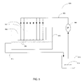
- FIG. 5 is a simplified schematic illustrating a set-up for cleaning silicon carbide wafer-lift pins, according to certain embodiments of the invention.
- the set-up 500 includes the following, according to certain embodiments:
- a reservoir 510 that contains an aqueous solution 512 of HF, HNO 3 , and H 2 O;
- a pump 508 which can be a peristaltic pump
- wafer-lift pins 502 are oriented on pin rack 504 such that pin heads 503 are at the bottom of the pin rack.
- Pump 508 pumps aqueous solution 512 from reservoir 510 through the manifold such that aqueous solution 512 fills the plenum of each wafer-lift pin to overflowing capacity.
- the overflow of aqueous solution 512 is collected at tank 516 and returned by return hose 514 to reservoir 510 .
- reservoir 510 , pump 508 , manifold 506 , pin rack 504 , tank 516 , and return hose 514 are all made of chemically resistant materials.
- a chemically resistant material is polyethylene.
- FIG. 6 is a simplified schematic illustrating a set-up adapted for cleaning a fixtured silicon carbide wafer-showerhead, according to certain embodiments of the invention.
- Set-up 600 of FIG. 6 includes the following, according to certain embodiments:
- fixture 604 that is secured to anodized aluminum base 602 via screws 606 a and 606 b;
- fixture 604 is needed to cover the anodized aluminum base 602 to prevent a chemical reaction between the anodized aluminum base 602 and aqueous solution 616 .
- O-ring 608 provides a seal between fixture 604 and the anodized aluminum base 602 .
- Fixture 604 and screws 606 a and 606 b are made of a chemically resistant material.
- the type of chemically resistant material may vary from implementation to implementation. According to certain embodiments, polyethylene may be used.
- Nitrogen gas stream 612 is used as a purge in order to prevent migration of aqueous solution 616 up to anodized aluminum base 602 through capillary action.
Landscapes
- Chemical & Material Sciences (AREA)
- Engineering & Computer Science (AREA)
- Ceramic Engineering (AREA)
- Materials Engineering (AREA)
- Structural Engineering (AREA)
- Organic Chemistry (AREA)
- Chemical Kinetics & Catalysis (AREA)
- General Chemical & Material Sciences (AREA)
- Mechanical Engineering (AREA)
- Cleaning Or Drying Semiconductors (AREA)
Abstract
Description
Claims (41)
Priority Applications (1)
| Application Number | Priority Date | Filing Date | Title |
|---|---|---|---|
| US10/696,394 US7754609B1 (en) | 2003-10-28 | 2003-10-28 | Cleaning processes for silicon carbide materials |
Applications Claiming Priority (1)
| Application Number | Priority Date | Filing Date | Title |
|---|---|---|---|
| US10/696,394 US7754609B1 (en) | 2003-10-28 | 2003-10-28 | Cleaning processes for silicon carbide materials |
Publications (1)
| Publication Number | Publication Date |
|---|---|
| US7754609B1 true US7754609B1 (en) | 2010-07-13 |
Family
ID=42314084
Family Applications (1)
| Application Number | Title | Priority Date | Filing Date |
|---|---|---|---|
| US10/696,394 Expired - Lifetime US7754609B1 (en) | 2003-10-28 | 2003-10-28 | Cleaning processes for silicon carbide materials |
Country Status (1)
| Country | Link |
|---|---|
| US (1) | US7754609B1 (en) |
Cited By (7)
| Publication number | Priority date | Publication date | Assignee | Title |
|---|---|---|---|---|
| US20130104942A1 (en) * | 2011-10-31 | 2013-05-02 | Lam Research Corporation | Mixed Acid Cleaning Assemblies |
| JP2013216525A (en) * | 2012-04-06 | 2013-10-24 | Bridgestone Corp | Method for manufacturing silicon carbide member |
| US20210249280A1 (en) * | 2018-05-29 | 2021-08-12 | Applied Materials, Inc. | Wet cleaning of electrostatic chuck |
| US20210283722A1 (en) * | 2020-06-11 | 2021-09-16 | Chongqing Institute Of East China Normal University | Device and method for precessing micro-channel on microfluidic chip using multi-focus ultrafast laser |
| US11264265B2 (en) * | 2017-02-02 | 2022-03-01 | Sumco Corporation | Lift pin, and epitaxial growth apparatus and method of producing silicon epitaxial wafer using the lift pin |
| US20240293850A1 (en) * | 2023-03-01 | 2024-09-05 | Lpe S.P.A. | Method for removing layers of silicon carbide, as well as process and apparatus for cleaning epitaxial reactor components |
| US12564871B2 (en) | 2020-12-02 | 2026-03-03 | Asm Ip Holding B.V. | Cleaning fixture for showerhead assemblies |
Citations (80)
| Publication number | Priority date | Publication date | Assignee | Title |
|---|---|---|---|---|
| US3775202A (en) | 1972-03-13 | 1973-11-27 | Dea Prod Inc | Etching control system |
| JPS5087974A (en) | 1973-12-09 | 1975-07-15 | ||
| US3969195A (en) | 1971-05-07 | 1976-07-13 | Siemens Aktiengesellschaft | Methods of coating and surface finishing articles made of metals and their alloys |
| US3986653A (en) | 1974-09-03 | 1976-10-19 | Tribotech | Method for coating bonding tools and product |
| US3992454A (en) | 1971-04-26 | 1976-11-16 | Joseph W. Aidlin | Protective coating for articles |
| US4023936A (en) | 1976-06-14 | 1977-05-17 | Lukens Steel Company | Titanium clad steel and process for making |
| US4078963A (en) | 1973-12-10 | 1978-03-14 | U.S. Philips Corporation | Method of manufacturing a semiconductor device, having a pattern of conductors on a supporting body |
| US4101386A (en) | 1971-05-07 | 1978-07-18 | Siemens Aktiengesellschaft | Methods of coating and surface finishing articles made of metals and their alloys |
| US4139348A (en) | 1975-11-28 | 1979-02-13 | Massachusetts Institute Of Technology | Electrochemical process and apparatus to control the chemical state of a material |
| US4197631A (en) | 1976-12-10 | 1980-04-15 | Bbc Brown Boveri & Company, Limited | Method of manufacturing semiconductor components |
| US4214952A (en) | 1978-02-28 | 1980-07-29 | Ngk Insulators, Ltd. | Electrochemical treatment process |
| US4232060A (en) | 1979-01-22 | 1980-11-04 | Richardson Chemical Company | Method of preparing substrate surface for electroless plating and products produced thereby |
| US4272612A (en) | 1979-05-09 | 1981-06-09 | The United States Of America As Represented By The Secretary Of The Army | Erosion lithography to abrade a pattern onto a substrate |
| US4327134A (en) | 1979-11-29 | 1982-04-27 | Alloy Surfaces Company, Inc. | Stripping of diffusion treated metals |
| US4367119A (en) | 1980-08-18 | 1983-01-04 | International Business Machines Corporation | Planar multi-level metal process with built-in etch stop |
| US4447824A (en) | 1980-08-18 | 1984-05-08 | International Business Machines Corporation | Planar multi-level metal process with built-in etch stop |
| US4448800A (en) | 1981-08-10 | 1984-05-15 | Nippon Telegraph And Telephone Public Corporation | Method for the manufacture of semiconductor device using refractory metal in a lift-off step |
| US4459155A (en) | 1981-01-10 | 1984-07-10 | The British Petroleum Company Limited | Method of producing corrosion inhibitors |
| US4519914A (en) | 1975-06-30 | 1985-05-28 | Kenji Etani | Method for treating swimming pool water |
| US4530120A (en) | 1975-06-30 | 1985-07-23 | Kenji Etani | Methods and apparatus for bathing |
| US4579569A (en) | 1982-10-14 | 1986-04-01 | Fume-Klean | Apparatus for neutralizing and removing fumes |
| US4638553A (en) | 1982-12-08 | 1987-01-27 | International Rectifier Corporation | Method of manufacture of semiconductor device |
| US4699082A (en) | 1983-02-25 | 1987-10-13 | Liburdi Engineering Limited | Apparatus for chemical vapor deposition |
| US4863561A (en) | 1986-12-09 | 1989-09-05 | Texas Instruments Incorporated | Method and apparatus for cleaning integrated circuit wafers |
| US4957583A (en) | 1989-04-28 | 1990-09-18 | Analog Devices, Inc. | Apparatus for etching patterned substrates |
| US4971590A (en) | 1987-12-02 | 1990-11-20 | Zenith Electronics Corporation | Process for improving the emissivity of a non-based tension shadow mask |
| US4980017A (en) | 1988-10-01 | 1990-12-25 | Nisso Engineering Company, Ltd. | Method for recirculating high-temperature etching solution |
| US5104501A (en) | 1989-06-13 | 1992-04-14 | Daicel Chemical Industries, Ltd. | Electrolytic cleaning method and electrolytic cleaning solution for stamper |
| US5152878A (en) | 1991-12-31 | 1992-10-06 | International Business Machines Corporation | Method for electrochemical cleaning of metal residue on molybdenum masks |
| US5221421A (en) | 1992-03-25 | 1993-06-22 | Hewlett-Packard Company | Controlled etching process for forming fine-geometry circuit lines on a substrate |
| US5365112A (en) | 1991-10-14 | 1994-11-15 | Kabushiki Kaisha Toshiba | Semiconductor integrated circuit device having an improved bonding pad structure |
| US5516399A (en) | 1994-06-30 | 1996-05-14 | International Business Machines Corporation | Contactless real-time in-situ monitoring of a chemical etching |
| US5593339A (en) | 1993-08-12 | 1997-01-14 | Church & Dwight Co., Inc. | Slurry cleaning process |
| US5614027A (en) | 1994-09-23 | 1997-03-25 | Church & Dwight Co., Inc. | Metal cleaner with novel anti-corrosion system |
| US5660640A (en) * | 1995-06-16 | 1997-08-26 | Joray Corporation | Method of removing sputter deposition from components of vacuum deposition equipment |
| US5665473A (en) | 1994-09-16 | 1997-09-09 | Tokuyama Corporation | Package for mounting a semiconductor device |
| US5712198A (en) | 1994-08-26 | 1998-01-27 | Memc Electronic Materials, Inc. | Pre-thermal treatment cleaning process |
| US5744214A (en) | 1997-01-30 | 1998-04-28 | International Business Machines Corporation | Corrosion resistant molybdenum mask |
| US5749467A (en) * | 1992-05-26 | 1998-05-12 | Empak, Inc. | Wafer suspension box |
| US5766979A (en) | 1996-11-08 | 1998-06-16 | W. L. Gore & Associates, Inc. | Wafer level contact sheet and method of assembly |
| US5840402A (en) | 1994-06-24 | 1998-11-24 | Sheldahl, Inc. | Metallized laminate material having ordered distribution of conductive through holes |
| US5863801A (en) * | 1996-06-14 | 1999-01-26 | Sarnoff Corporation | Automated nucleic acid isolation |
| US5882598A (en) * | 1995-06-09 | 1999-03-16 | Scp Global Technologies | Wafer gap conductivity cell for characterizing process vessels and semiconductor fabrication processes and method of use |
| US5888308A (en) | 1997-02-28 | 1999-03-30 | International Business Machines Corporation | Process for removing residue from screening masks with alkaline solution |
| US5891354A (en) | 1996-07-26 | 1999-04-06 | Fujitsu Limited | Methods of etching through wafers and substrates with a composite etch stop layer |
| US5908819A (en) | 1997-05-06 | 1999-06-01 | Church & Dwight Co., Inc. | Aqueous cleaning composition for cleaning substrates and method of using same |
| US5929521A (en) | 1997-03-26 | 1999-07-27 | Micron Technology, Inc. | Projected contact structure for bumped semiconductor device and resulting articles and assemblies |
| US5966593A (en) | 1996-11-08 | 1999-10-12 | W. L. Gore & Associates, Inc. | Method of forming a wafer level contact sheet having a permanent z-axis material |
| JPH11290805A (en) | 1998-04-15 | 1999-10-26 | Tietech Co Ltd | Metal mask cleaning equipment |
| US6012966A (en) | 1996-05-10 | 2000-01-11 | Canon Kabushiki Kaisha | Precision polishing apparatus with detecting means |
| US6083320A (en) * | 1997-02-28 | 2000-07-04 | Samsung Electronics Co., Ltd. | Robot for and method of transporting semiconductor wafers |
| US6147003A (en) * | 1997-05-06 | 2000-11-14 | Yamaha Corporation | Method of manufacturing semiconductor device |
| US6187216B1 (en) | 1997-08-27 | 2001-02-13 | Motorola, Inc. | Method for etching a dielectric layer over a semiconductor substrate |
| US6199563B1 (en) * | 1997-02-21 | 2001-03-13 | Canon Kabushiki Kaisha | Wafer processing apparatus, wafer processing method, and semiconductor substrate fabrication method |
| US6273950B1 (en) * | 1996-04-18 | 2001-08-14 | Matsushita Electric Industrial Co., Ltd. | SiC device and method for manufacturing the same |
| TW460611B (en) | 1999-05-26 | 2001-10-21 | Winbond Electronics Corp | Process for cleaning showerhead for a chemical vapor deposition chamber |
| WO2002015255A1 (en) * | 2000-08-11 | 2002-02-21 | Chem Trace Corporation | System and method for cleaning semiconductor fabrication equipment parts |
| US6352081B1 (en) * | 1999-07-09 | 2002-03-05 | Applied Materials, Inc. | Method of cleaning a semiconductor device processing chamber after a copper etch process |
| US6368410B1 (en) | 1999-06-28 | 2002-04-09 | General Electric Company | Semiconductor processing article |
| US6375752B1 (en) * | 1999-06-29 | 2002-04-23 | Bridgestone Corporation | Method of wet-cleaning sintered silicon carbide |
| US6394023B1 (en) | 2000-03-27 | 2002-05-28 | Applied Materials, Inc. | Process kit parts and method for using same |
| US6419757B2 (en) * | 1998-12-08 | 2002-07-16 | Bridgestone, Corporation | Method for cleaning sintered silicon carbide in wet condition |
| US6475444B1 (en) | 1999-07-19 | 2002-11-05 | Cybio Instruments Gmbh | Rinsing tray system |
| US6488037B1 (en) * | 1999-08-31 | 2002-12-03 | Texas Instruments Incorporated | Programmable physical action during integrated circuit wafer cleanup |
| US20030000458A1 (en) | 2000-02-07 | 2003-01-02 | Yoshinori Marumo | Quartz member for semiconductor manufacturing equipment and method for metal analysis in quartz member |
| US6506254B1 (en) | 2000-06-30 | 2003-01-14 | Lam Research Corporation | Semiconductor processing equipment having improved particle performance |
| US20030096562A1 (en) | 2001-04-11 | 2003-05-22 | Olympus Optical Co., Ltd. | Polishing apparatus, polishing method, control program for causing computer to execute polishing, and recording medium |
| US6569252B1 (en) | 2000-06-30 | 2003-05-27 | International Business Machines Corporation | Semi-aqueous solvent cleaning of paste processing residue from substrates |
| US6579153B2 (en) | 2000-01-12 | 2003-06-17 | Jsr Corporation | Aqueous dispersion for chemical mechanical polishing and chemical mechanical polishing process |
| US20030136428A1 (en) | 2002-01-23 | 2003-07-24 | Applied Materials, Inc. | Cleaning process residues on a process chamber component |
| US6607605B2 (en) | 2000-08-31 | 2003-08-19 | Chemtrace Corporation | Cleaning of semiconductor process equipment chamber parts using organic solvents |
| US20030183244A1 (en) | 2002-04-02 | 2003-10-02 | Applied Materials, Inc. | Method of cleaning a semiconductor processing chamber |
| US20040060579A1 (en) | 2002-06-24 | 2004-04-01 | Jaung-Joo Kim | Cleaning solution and method for cleaning ceramic parts using the same |
| US6767840B1 (en) | 1997-02-21 | 2004-07-27 | Canon Kabushiki Kaisha | Wafer processing apparatus, wafer processing method, and semiconductor substrate fabrication method |
| US20050016565A1 (en) | 2003-07-24 | 2005-01-27 | Tan Samantha S.H. | Cleaning masks |
| US20050050708A1 (en) | 2003-09-04 | 2005-03-10 | Taiwan Semiconductor Manufacturing Co., Ltd. | Embedded fastener apparatus and method for preventing particle contamination |
| US20050173569A1 (en) | 2004-02-05 | 2005-08-11 | Applied Materials, Inc. | Gas distribution showerhead for semiconductor processing |
| US7045072B2 (en) | 2003-07-24 | 2006-05-16 | Tan Samantha S H | Cleaning process and apparatus for silicate materials |
| US20080099054A1 (en) | 2006-11-01 | 2008-05-01 | Felix Rabinovich | Methods and apparatus for cleaning chamber components |
| US20090197004A1 (en) | 2007-12-19 | 2009-08-06 | Applied Materials, Inc. | Methods for cleaning process kits and chambers, and for ruthenium recovery |
-
2003
- 2003-10-28 US US10/696,394 patent/US7754609B1/en not_active Expired - Lifetime
Patent Citations (82)
| Publication number | Priority date | Publication date | Assignee | Title |
|---|---|---|---|---|
| US3992454A (en) | 1971-04-26 | 1976-11-16 | Joseph W. Aidlin | Protective coating for articles |
| US3969195A (en) | 1971-05-07 | 1976-07-13 | Siemens Aktiengesellschaft | Methods of coating and surface finishing articles made of metals and their alloys |
| US4101386A (en) | 1971-05-07 | 1978-07-18 | Siemens Aktiengesellschaft | Methods of coating and surface finishing articles made of metals and their alloys |
| US3775202A (en) | 1972-03-13 | 1973-11-27 | Dea Prod Inc | Etching control system |
| JPS5087974A (en) | 1973-12-09 | 1975-07-15 | ||
| US4078963A (en) | 1973-12-10 | 1978-03-14 | U.S. Philips Corporation | Method of manufacturing a semiconductor device, having a pattern of conductors on a supporting body |
| US3986653A (en) | 1974-09-03 | 1976-10-19 | Tribotech | Method for coating bonding tools and product |
| US4519914A (en) | 1975-06-30 | 1985-05-28 | Kenji Etani | Method for treating swimming pool water |
| US4530120A (en) | 1975-06-30 | 1985-07-23 | Kenji Etani | Methods and apparatus for bathing |
| US4139348A (en) | 1975-11-28 | 1979-02-13 | Massachusetts Institute Of Technology | Electrochemical process and apparatus to control the chemical state of a material |
| US4023936A (en) | 1976-06-14 | 1977-05-17 | Lukens Steel Company | Titanium clad steel and process for making |
| US4197631A (en) | 1976-12-10 | 1980-04-15 | Bbc Brown Boveri & Company, Limited | Method of manufacturing semiconductor components |
| US4214952A (en) | 1978-02-28 | 1980-07-29 | Ngk Insulators, Ltd. | Electrochemical treatment process |
| US4232060A (en) | 1979-01-22 | 1980-11-04 | Richardson Chemical Company | Method of preparing substrate surface for electroless plating and products produced thereby |
| US4272612A (en) | 1979-05-09 | 1981-06-09 | The United States Of America As Represented By The Secretary Of The Army | Erosion lithography to abrade a pattern onto a substrate |
| US4327134A (en) | 1979-11-29 | 1982-04-27 | Alloy Surfaces Company, Inc. | Stripping of diffusion treated metals |
| US4367119A (en) | 1980-08-18 | 1983-01-04 | International Business Machines Corporation | Planar multi-level metal process with built-in etch stop |
| US4447824A (en) | 1980-08-18 | 1984-05-08 | International Business Machines Corporation | Planar multi-level metal process with built-in etch stop |
| US4459155A (en) | 1981-01-10 | 1984-07-10 | The British Petroleum Company Limited | Method of producing corrosion inhibitors |
| US4448800A (en) | 1981-08-10 | 1984-05-15 | Nippon Telegraph And Telephone Public Corporation | Method for the manufacture of semiconductor device using refractory metal in a lift-off step |
| US4579569A (en) | 1982-10-14 | 1986-04-01 | Fume-Klean | Apparatus for neutralizing and removing fumes |
| US4638553A (en) | 1982-12-08 | 1987-01-27 | International Rectifier Corporation | Method of manufacture of semiconductor device |
| US4699082A (en) | 1983-02-25 | 1987-10-13 | Liburdi Engineering Limited | Apparatus for chemical vapor deposition |
| US4863561A (en) | 1986-12-09 | 1989-09-05 | Texas Instruments Incorporated | Method and apparatus for cleaning integrated circuit wafers |
| US4971590A (en) | 1987-12-02 | 1990-11-20 | Zenith Electronics Corporation | Process for improving the emissivity of a non-based tension shadow mask |
| US4980017A (en) | 1988-10-01 | 1990-12-25 | Nisso Engineering Company, Ltd. | Method for recirculating high-temperature etching solution |
| US4957583A (en) | 1989-04-28 | 1990-09-18 | Analog Devices, Inc. | Apparatus for etching patterned substrates |
| US5104501A (en) | 1989-06-13 | 1992-04-14 | Daicel Chemical Industries, Ltd. | Electrolytic cleaning method and electrolytic cleaning solution for stamper |
| US5365112A (en) | 1991-10-14 | 1994-11-15 | Kabushiki Kaisha Toshiba | Semiconductor integrated circuit device having an improved bonding pad structure |
| US5152878A (en) | 1991-12-31 | 1992-10-06 | International Business Machines Corporation | Method for electrochemical cleaning of metal residue on molybdenum masks |
| US5221421A (en) | 1992-03-25 | 1993-06-22 | Hewlett-Packard Company | Controlled etching process for forming fine-geometry circuit lines on a substrate |
| US5749467A (en) * | 1992-05-26 | 1998-05-12 | Empak, Inc. | Wafer suspension box |
| US5593339A (en) | 1993-08-12 | 1997-01-14 | Church & Dwight Co., Inc. | Slurry cleaning process |
| US5840402A (en) | 1994-06-24 | 1998-11-24 | Sheldahl, Inc. | Metallized laminate material having ordered distribution of conductive through holes |
| US5516399A (en) | 1994-06-30 | 1996-05-14 | International Business Machines Corporation | Contactless real-time in-situ monitoring of a chemical etching |
| US5712198A (en) | 1994-08-26 | 1998-01-27 | Memc Electronic Materials, Inc. | Pre-thermal treatment cleaning process |
| US5665473A (en) | 1994-09-16 | 1997-09-09 | Tokuyama Corporation | Package for mounting a semiconductor device |
| US5614027A (en) | 1994-09-23 | 1997-03-25 | Church & Dwight Co., Inc. | Metal cleaner with novel anti-corrosion system |
| US5882598A (en) * | 1995-06-09 | 1999-03-16 | Scp Global Technologies | Wafer gap conductivity cell for characterizing process vessels and semiconductor fabrication processes and method of use |
| US5660640A (en) * | 1995-06-16 | 1997-08-26 | Joray Corporation | Method of removing sputter deposition from components of vacuum deposition equipment |
| US6273950B1 (en) * | 1996-04-18 | 2001-08-14 | Matsushita Electric Industrial Co., Ltd. | SiC device and method for manufacturing the same |
| US6012966A (en) | 1996-05-10 | 2000-01-11 | Canon Kabushiki Kaisha | Precision polishing apparatus with detecting means |
| US5863801A (en) * | 1996-06-14 | 1999-01-26 | Sarnoff Corporation | Automated nucleic acid isolation |
| US5891354A (en) | 1996-07-26 | 1999-04-06 | Fujitsu Limited | Methods of etching through wafers and substrates with a composite etch stop layer |
| US5966593A (en) | 1996-11-08 | 1999-10-12 | W. L. Gore & Associates, Inc. | Method of forming a wafer level contact sheet having a permanent z-axis material |
| US5766979A (en) | 1996-11-08 | 1998-06-16 | W. L. Gore & Associates, Inc. | Wafer level contact sheet and method of assembly |
| US5744214A (en) | 1997-01-30 | 1998-04-28 | International Business Machines Corporation | Corrosion resistant molybdenum mask |
| US6199563B1 (en) * | 1997-02-21 | 2001-03-13 | Canon Kabushiki Kaisha | Wafer processing apparatus, wafer processing method, and semiconductor substrate fabrication method |
| US6767840B1 (en) | 1997-02-21 | 2004-07-27 | Canon Kabushiki Kaisha | Wafer processing apparatus, wafer processing method, and semiconductor substrate fabrication method |
| US5888308A (en) | 1997-02-28 | 1999-03-30 | International Business Machines Corporation | Process for removing residue from screening masks with alkaline solution |
| US6083320A (en) * | 1997-02-28 | 2000-07-04 | Samsung Electronics Co., Ltd. | Robot for and method of transporting semiconductor wafers |
| US5929521A (en) | 1997-03-26 | 1999-07-27 | Micron Technology, Inc. | Projected contact structure for bumped semiconductor device and resulting articles and assemblies |
| US6147003A (en) * | 1997-05-06 | 2000-11-14 | Yamaha Corporation | Method of manufacturing semiconductor device |
| US5908819A (en) | 1997-05-06 | 1999-06-01 | Church & Dwight Co., Inc. | Aqueous cleaning composition for cleaning substrates and method of using same |
| US6187216B1 (en) | 1997-08-27 | 2001-02-13 | Motorola, Inc. | Method for etching a dielectric layer over a semiconductor substrate |
| JPH11290805A (en) | 1998-04-15 | 1999-10-26 | Tietech Co Ltd | Metal mask cleaning equipment |
| US6419757B2 (en) * | 1998-12-08 | 2002-07-16 | Bridgestone, Corporation | Method for cleaning sintered silicon carbide in wet condition |
| TW460611B (en) | 1999-05-26 | 2001-10-21 | Winbond Electronics Corp | Process for cleaning showerhead for a chemical vapor deposition chamber |
| US6368410B1 (en) | 1999-06-28 | 2002-04-09 | General Electric Company | Semiconductor processing article |
| US6375752B1 (en) * | 1999-06-29 | 2002-04-23 | Bridgestone Corporation | Method of wet-cleaning sintered silicon carbide |
| US6352081B1 (en) * | 1999-07-09 | 2002-03-05 | Applied Materials, Inc. | Method of cleaning a semiconductor device processing chamber after a copper etch process |
| US6475444B1 (en) | 1999-07-19 | 2002-11-05 | Cybio Instruments Gmbh | Rinsing tray system |
| US6488037B1 (en) * | 1999-08-31 | 2002-12-03 | Texas Instruments Incorporated | Programmable physical action during integrated circuit wafer cleanup |
| US6579153B2 (en) | 2000-01-12 | 2003-06-17 | Jsr Corporation | Aqueous dispersion for chemical mechanical polishing and chemical mechanical polishing process |
| US20030000458A1 (en) | 2000-02-07 | 2003-01-02 | Yoshinori Marumo | Quartz member for semiconductor manufacturing equipment and method for metal analysis in quartz member |
| US6394023B1 (en) | 2000-03-27 | 2002-05-28 | Applied Materials, Inc. | Process kit parts and method for using same |
| US6569252B1 (en) | 2000-06-30 | 2003-05-27 | International Business Machines Corporation | Semi-aqueous solvent cleaning of paste processing residue from substrates |
| US6506254B1 (en) | 2000-06-30 | 2003-01-14 | Lam Research Corporation | Semiconductor processing equipment having improved particle performance |
| WO2002015255A1 (en) * | 2000-08-11 | 2002-02-21 | Chem Trace Corporation | System and method for cleaning semiconductor fabrication equipment parts |
| US6810887B2 (en) | 2000-08-11 | 2004-11-02 | Chemtrace Corporation | Method for cleaning semiconductor fabrication equipment parts |
| US6607605B2 (en) | 2000-08-31 | 2003-08-19 | Chemtrace Corporation | Cleaning of semiconductor process equipment chamber parts using organic solvents |
| US20030096562A1 (en) | 2001-04-11 | 2003-05-22 | Olympus Optical Co., Ltd. | Polishing apparatus, polishing method, control program for causing computer to execute polishing, and recording medium |
| US20030136428A1 (en) | 2002-01-23 | 2003-07-24 | Applied Materials, Inc. | Cleaning process residues on a process chamber component |
| US20030183244A1 (en) | 2002-04-02 | 2003-10-02 | Applied Materials, Inc. | Method of cleaning a semiconductor processing chamber |
| US20040060579A1 (en) | 2002-06-24 | 2004-04-01 | Jaung-Joo Kim | Cleaning solution and method for cleaning ceramic parts using the same |
| US20050016565A1 (en) | 2003-07-24 | 2005-01-27 | Tan Samantha S.H. | Cleaning masks |
| US7045072B2 (en) | 2003-07-24 | 2006-05-16 | Tan Samantha S H | Cleaning process and apparatus for silicate materials |
| US7091132B2 (en) | 2003-07-24 | 2006-08-15 | Applied Materials, Inc. | Ultrasonic assisted etch using corrosive liquids |
| US20050050708A1 (en) | 2003-09-04 | 2005-03-10 | Taiwan Semiconductor Manufacturing Co., Ltd. | Embedded fastener apparatus and method for preventing particle contamination |
| US20050173569A1 (en) | 2004-02-05 | 2005-08-11 | Applied Materials, Inc. | Gas distribution showerhead for semiconductor processing |
| US20080099054A1 (en) | 2006-11-01 | 2008-05-01 | Felix Rabinovich | Methods and apparatus for cleaning chamber components |
| US20090197004A1 (en) | 2007-12-19 | 2009-08-06 | Applied Materials, Inc. | Methods for cleaning process kits and chambers, and for ruthenium recovery |
Non-Patent Citations (5)
| Title |
|---|
| Dewent. Englsih Abstract of TW 460611 A (2001). * |
| Hoffman, H.S., Molybdenum Cleaning Solution, IBM Technical Disclosure Bulletin, 3(5):36, (1960). |
| Metrology for Manufacturing: Surface Measurement. [online] Michigan Technological University, undated [retrieved on Aug. 9, 2005]. Retrieved from the Internet: . |
| Metrology for Manufacturing: Surface Measurement. [online] Michigan Technological University, undated [retrieved on Aug. 9, 2005]. Retrieved from the Internet: <URL: http://www.mfg.mtu.edu/cyberman/quality/metrology/surface.html>. |
| Spring, S., Metal Cleaning, Reinhold Publishing Corporation, New York, pp. 85-89, (1963). |
Cited By (11)
| Publication number | Priority date | Publication date | Assignee | Title |
|---|---|---|---|---|
| US20130104942A1 (en) * | 2011-10-31 | 2013-05-02 | Lam Research Corporation | Mixed Acid Cleaning Assemblies |
| US9293305B2 (en) * | 2011-10-31 | 2016-03-22 | Lam Research Corporation | Mixed acid cleaning assemblies |
| JP2013216525A (en) * | 2012-04-06 | 2013-10-24 | Bridgestone Corp | Method for manufacturing silicon carbide member |
| US11264265B2 (en) * | 2017-02-02 | 2022-03-01 | Sumco Corporation | Lift pin, and epitaxial growth apparatus and method of producing silicon epitaxial wafer using the lift pin |
| US20210249280A1 (en) * | 2018-05-29 | 2021-08-12 | Applied Materials, Inc. | Wet cleaning of electrostatic chuck |
| US11776822B2 (en) * | 2018-05-29 | 2023-10-03 | Applied Materials, Inc. | Wet cleaning of electrostatic chuck |
| US20210283722A1 (en) * | 2020-06-11 | 2021-09-16 | Chongqing Institute Of East China Normal University | Device and method for precessing micro-channel on microfluidic chip using multi-focus ultrafast laser |
| US12090576B2 (en) * | 2020-06-11 | 2024-09-17 | Chongqing Institute Of East China Normal University | Device and method for processing micro-channel on microfluidic chip using multi-focus ultrafast laser |
| US12564871B2 (en) | 2020-12-02 | 2026-03-03 | Asm Ip Holding B.V. | Cleaning fixture for showerhead assemblies |
| US20240293850A1 (en) * | 2023-03-01 | 2024-09-05 | Lpe S.P.A. | Method for removing layers of silicon carbide, as well as process and apparatus for cleaning epitaxial reactor components |
| US12485458B2 (en) * | 2023-03-01 | 2025-12-02 | Lpe S.P.A. | Method for removing layers of silicon carbide, as well as process and apparatus for cleaning epitaxial reactor components |
Similar Documents
| Publication | Publication Date | Title |
|---|---|---|
| TWI266811B (en) | Cleaning method for thin film formation system | |
| KR100385255B1 (en) | Method of cleaning porous body, and process for producing porous body, non-porous film or bonded substrate | |
| CN107946163B (en) | Chemical conversion of yttrium oxide to yttrium fluoride and yttrium oxyfluoride to develop anticorrosion coatings for pretreatment of plasma components | |
| JP5324160B2 (en) | Wet clean process for regenerating anodizing chamber parts | |
| US6899767B2 (en) | Method of cleaning processing chamber of semiconductor processing apparatus | |
| CN1179394C (en) | Wafer cleaning and vapor drying systems and methods | |
| US5723019A (en) | Drip chemical delivery method and apparatus | |
| KR102059692B1 (en) | Method of cleaning aluminum plasma chamber parts | |
| TWI752475B (en) | Etching apparatus and etching method thereof | |
| US10777405B2 (en) | Drying process for high aspect ratio features | |
| JPH10275798A (en) | Anodizing apparatus and related apparatus and method | |
| CN1622281A (en) | Method for producing semiconductor device and cleaning device for resist stripping | |
| US6825123B2 (en) | Method for treating semiconductor processing components and components formed thereby | |
| US7754609B1 (en) | Cleaning processes for silicon carbide materials | |
| US12094732B2 (en) | Substrate processing method and substrate processing apparatus | |
| KR20120102707A (en) | Methodology for cleaning of surface metal contamination from an upper electrode used in a plasma chamber | |
| KR20090091153A (en) | Method and apparatus for cleaning chamber parts | |
| WO2005054543A1 (en) | Cleaning method | |
| TWI878006B (en) | Substrate processing method and substrate processing apparatus | |
| TWI385720B (en) | Etching composition and etching treatment method | |
| JP2007142335A (en) | High pressure processing method | |
| TW453904B (en) | Method for cleaning semiconductor wafer surface | |
| JP4748581B2 (en) | Vacuum processing apparatus and vacuum processing method | |
| US20020023663A1 (en) | Apparatus and method for preventing the re-adherence of particles in wafer-cleaning process | |
| KR20060002807A (en) | How to clean the heat treatment device |
Legal Events
| Date | Code | Title | Description |
|---|---|---|---|
| AS | Assignment |
Owner name: CHEMTRACE CORPORATION, CALIFORNIA Free format text: ASSIGNMENT OF ASSIGNORS INTEREST;ASSIGNOR:TAN, SAMANTHA S.H.;REEL/FRAME:015157/0518 Effective date: 20040308 |
|
| AS | Assignment |
Owner name: CHEMTRACE PRECISION CLEANING, INC., CALIFORNIA Free format text: ASSIGNMENT OF ASSIGNORS INTEREST;ASSIGNOR:CHEMTRACE CORPORATION;REEL/FRAME:015260/0197 Effective date: 20041008 |
|
| AS | Assignment |
Owner name: METRON TECHNOLOGY DISTRIBUTION CORPORATION, CALIFO Free format text: MERGER;ASSIGNOR:CHEMTRACE PRECISION CLEANING, INC.;REEL/FRAME:024389/0976 Effective date: 20071025 Owner name: METRON TECHNOLOGY CORPORATION, CALIFORNIA Free format text: MERGER;ASSIGNOR:METRON TECHNOLOGY DISTRIBUTION CORPORATION;REEL/FRAME:024389/0982 Effective date: 20071025 Owner name: APPLIED MATERIALS, INC., CALIFORNIA Free format text: MERGER;ASSIGNOR:METRON TECHNOLOGY CORPORATION;REEL/FRAME:024389/0988 Effective date: 20071025 |
|
| STCF | Information on status: patent grant |
Free format text: PATENTED CASE |
|
| AS | Assignment |
Owner name: FOX CHASE BANK, PENNSYLVANIA Free format text: SECURITY AGREEMENT;ASSIGNOR:QUANTUM GLOBAL TECHNOLOGIES, LLC;REEL/FRAME:026468/0130 Effective date: 20110609 |
|
| AS | Assignment |
Owner name: QUANTUM GLOBAL TECHNOLOGIES LLC, PENNSYLVANIA Free format text: ASSIGNMENT OF ASSIGNORS INTEREST;ASSIGNOR:APPLIED MATERIALS, INC.;REEL/FRAME:026886/0171 Effective date: 20110512 |
|
| FPAY | Fee payment |
Year of fee payment: 4 |
|
| MAFP | Maintenance fee payment |
Free format text: PAYMENT OF MAINTENANCE FEE, 8TH YEAR, LARGE ENTITY (ORIGINAL EVENT CODE: M1552) Year of fee payment: 8 |
|
| AS | Assignment |
Owner name: BARCLAYS BANK PLC, AS ADMINISTRATIVE AGENT, NEW YO Free format text: SECURITY INTEREST;ASSIGNORS:ULTRA CLEAN HOLDINGS, INC.;UCT THERMAL SOLUTIONS, INC.;ULTRA CLEAN TECHNOLOGY SYSTEMS AND SERVICE, INC.;AND OTHERS;REEL/FRAME:048175/0960 Effective date: 20180827 |
|
| AS | Assignment |
Owner name: QUANTUM GLOBAL TECHNOLOGIES, LLC, PENNSYLVANIA Free format text: RELEASE BY SECURED PARTY;ASSIGNOR:UNIVEST BANK AND TRUST CO., SUCCESSOR BY MERGER TO FOX CHASE BANK;REEL/FRAME:046962/0614 Effective date: 20180827 |
|
| MAFP | Maintenance fee payment |
Free format text: PAYMENT OF MAINTENANCE FEE, 12TH YEAR, LARGE ENTITY (ORIGINAL EVENT CODE: M1553); ENTITY STATUS OF PATENT OWNER: LARGE ENTITY Year of fee payment: 12 |