US7732239B2 - Method for manufacturing solid-state image sensor - Google Patents
Method for manufacturing solid-state image sensor Download PDFInfo
- Publication number
- US7732239B2 US7732239B2 US12/050,930 US5093008A US7732239B2 US 7732239 B2 US7732239 B2 US 7732239B2 US 5093008 A US5093008 A US 5093008A US 7732239 B2 US7732239 B2 US 7732239B2
- Authority
- US
- United States
- Prior art keywords
- region
- photoresist
- over
- dividing line
- regions
- Prior art date
- Legal status (The legal status is an assumption and is not a legal conclusion. Google has not performed a legal analysis and makes no representation as to the accuracy of the status listed.)
- Active, expires
Links
Images


Classifications
-
- H—ELECTRICITY
- H10—SEMICONDUCTOR DEVICES; ELECTRIC SOLID-STATE DEVICES NOT OTHERWISE PROVIDED FOR
- H10F—INORGANIC SEMICONDUCTOR DEVICES SENSITIVE TO INFRARED RADIATION, LIGHT, ELECTROMAGNETIC RADIATION OF SHORTER WAVELENGTH OR CORPUSCULAR RADIATION
- H10F39/00—Integrated devices, or assemblies of multiple devices, comprising at least one element covered by group H10F30/00, e.g. radiation detectors comprising photodiode arrays
- H10F39/80—Constructional details of image sensors
- H10F39/802—Geometry or disposition of elements in pixels, e.g. address-lines or gate electrodes
-
- H—ELECTRICITY
- H10—SEMICONDUCTOR DEVICES; ELECTRIC SOLID-STATE DEVICES NOT OTHERWISE PROVIDED FOR
- H10F—INORGANIC SEMICONDUCTOR DEVICES SENSITIVE TO INFRARED RADIATION, LIGHT, ELECTROMAGNETIC RADIATION OF SHORTER WAVELENGTH OR CORPUSCULAR RADIATION
- H10F39/00—Integrated devices, or assemblies of multiple devices, comprising at least one element covered by group H10F30/00, e.g. radiation detectors comprising photodiode arrays
- H10F39/011—Manufacture or treatment of image sensors covered by group H10F39/12
- H10F39/014—Manufacture or treatment of image sensors covered by group H10F39/12 of CMOS image sensors
Definitions
- the present invention relates to a solid-state image sensor and a manufacturing method thereof.
- the plural pixels are placed as densely as possible for the miniaturization of the device so that the above-described misalignment of resist patterns has a serious influence on the properties of the pixels and it is very important how to set the position of the dividing line for divided exposure.
- a first object of the invention is to provide a divided exposure technology capable of preventing deterioration in the performance of a solid-stage image sensor.
- a second object is to provide a technology facilitating grasping of the position of an exposure dividing line for divided exposure treatment.
- a semiconductor substrate is provided first.
- a photoresist is then formed over a semiconductor substrate via a protective film.
- the photoresist is then exposed using a photomask.
- the photoresist is subjected to divided exposure. Described specifically, the photoresist is divided into a plurality of exposure regions and exposure treatment is given to each of the plural exposure regions.
- the dividing line therefor is positioned at least over a region of the semiconductor substrate in which active regions in which pixels are to be formed are defined.
- the photoresist thus exposed is then developed and patterned.
- the protective film exposed from the patterned photoresist is removed and then, the photoresist is removed.
- the semiconductor substrate exposed from the protective film is then oxidized and an element isolation structure is formed in the semiconductor substrate, whereby in the semiconductor substrate, active regions in which pixel regions are to be formed are defined by the element isolation structure.
- the solid-state image sensor according to the one aspect of the present invention is equipped with a semiconductor substrate in which active regions are defined by an element isolation structure and pixels formed in the active regions.
- the active regions have a plurality of partial active regions in which impurity regions have been formed, respectively.
- the plural partial active regions include a partial active region having a shape displaced in one direction, in a top view, so as to cause a step difference at the periphery, in a top view.
- the dividing line therefor is located at least over a region of the semiconductor substrate in which the active regions are defined. Compared with a case where the dividing line is located only over a region of the semiconductor substrate in which an element isolation structure is to be formed, a portion of the element isolation structure which undergoes a dimensional change can be made smaller.
- a dimensional change in the element isolation structure may lead to deterioration of electrical insulation properties between devices so that deterioration of the performance of the solid-state image sensor can be suppressed by minimizing a portion of the element isolation structure which undergoes a dimensional change.
- the active regions in which pixels are to be formed include partial active regions having a shape displaced in one direction, in a top view, so as to cause a step difference at the periphery, in a top view.
- the active regions are defined in the semiconductor substrate and the photoresist is subjected to divided exposure with the position of the step difference of the partial active region as a boundary, it is possible to grasp the position of the dividing line for divided exposure readily by detecting the step difference.
- FIG. 1 illustrates the construction of a solid-state image sensor according to an embodiment of the present invention
- FIG. 2 illustrates the circuit construction of a pixel according to the embodiment of the present invention
- FIG. 3 is a top view illustrating the structure of the pixel according to the embodiment of the present invention.
- FIG. 4 is a top view illustrating the structure of the pixel according to the embodiment of the present invention.
- FIG. 5 is a cross-sectional view illustrating the structure of the pixel according to the embodiment of the present invention.
- FIG. 6 is a flow chart showing a manufacturing method of the solid-state image sensor according to the embodiment of the present invention.
- FIG. 7 illustrates divided exposure treatment in the embodiment of the present invention
- FIG. 8 is a flow chart showing a manufacturing method of an element isolation structure according to the embodiment of the present invention.
- FIG. 9 is a top view illustrating a manufacturing step of the element isolation structure according to the embodiment of the present invention.
- FIG. 10 is a top view illustrating a manufacturing step of the element isolation structure according to the embodiment of the present invention.
- FIG. 11 is a top view illustrating a manufacturing step of the element isolation structure according to the embodiment of the present invention.
- FIG. 12 is a flow chart showing a manufacturing method of a gate structure according to the embodiment of the present invention.
- FIG. 13 is a top view illustrating a manufacturing step of the gate structure according to the embodiment of the present invention.
- FIG. 14 is a top view illustrating a manufacturing step of the gate structure according to the embodiment of the present invention.
- FIG. 15 is a top view illustrating a manufacturing step of the gate structure according to the embodiment of the present invention.
- FIG. 16 is a top view illustrating a manufacturing step of the gate structure according to the embodiment of the present invention.
- FIG. 17 is a flow chart showing a manufacturing method of an impurity region according to the embodiment of the present invention.
- FIG. 18 is a top view illustrating a manufacturing step of the impurity region according to the embodiment of the present invention.
- FIG. 19 is a top view illustrating a manufacturing step of the impurity region according to the embodiment of the present invention.
- FIG. 20 is a top view illustrating a manufacturing step of the impurity region according to the embodiment of the present invention.
- FIG. 21 is a flow chart showing a manufacturing method of a contact plug and via plug according to the embodiment of the present invention.
- FIG. 22 is a top view illustrating a manufacturing step of the contact plug according to the embodiment of the present invention.
- FIG. 23 is a flow chart showing a manufacturing method of an interconnect according to the embodiment of the present invention.
- FIG. 24 is a top view illustrating a manufacturing step of the interconnect according to the embodiment of the present invention.
- FIG. 25 is a top view illustrating a manufacturing step of the interconnect according to the embodiment of the present invention.
- FIG. 26 is a top view illustrating a manufacturing step of the interconnect according to the embodiment of the present invention.
- FIG. 27 is a top view showing how a variation amount of the surface area of a partial active region differs, depending on the position of a dividing line for divided exposure;
- FIG. 28 is a top view for describing a reduction in the yield due to a positional change of a dividing line for divided exposure.
- FIG. 29 is a top view illustrating a modification example of the manufacturing step of the impurity region according to the embodiment of the present invention.
- FIG. 1 illustrates the construction of the solid-state image sensor according to one embodiment of the present invention.
- the solid-state image sensor according to this embodiment is a CMOS image sensor. As illustrated in FIG. 1 , is has a pixel array portion 1 , readout circuits 2 , 3 , output circuit 4 , row select circuit 5 , and control circuit 6 .
- a plurality of pixels 10 are arranged in a matrix.
- the X axis direction in FIG. 1 is a direction of a row in which pixels 10 are arranged, while the Y axis direction vertical to the X axis direction is a direction of a column in which pixels 10 are arranged.
- the plural pixels 10 each produces a signal according to the intensity of light irradiated.
- the row select circuit 5 selects a plurality of pixels 10 by the row.
- the pixels 10 selected by the row select circuit 5 output the produced signal to an output line OL which will be described later.
- the readout circuits 2 and 3 are placed opposite to each other in the Y axis direction while sandwiching the pixel array portion 1 between them.
- the readout circuits 2 and 3 each reads the signal output to the output line OL from the pixel 10 and then, outputs it to the output circuit 4 .
- the readout circuit 2 reads the signals of half of the pixels 10 which are on the side of the readout circuit 2
- the readout circuit 3 reads the signals of the other half of the pixels 10 which are on the side of the readout circuit 3 .
- the output circuit 4 outputs the signals of the pixels 10 read by the readout circuits 2 and 3 to the outside of the solid-state image sensor.
- the control circuit 6 totally manages the operation of the whole solid-state image sensor and controls the operation of the other constituents of the solid-state image sensor.
- FIG. 2 illustrates the circuit construction of each pixel 10 .
- the pixel 10 is equipped with a photodiode PD for performing photoelectric conversion, a transfer transistor TX for transferring charges generated at the photodiode PD, a floating diffusion FD for accumulating therein charges transferred from the transfer transistor TX, an amplified MOS imager transistor AMI for amplifying the potential of the floating diffusion FD, a select transistor SEL for selecting whether the potential amplified by the amplified MOS imager transistor AMI is output to the output line OL coupled to one of the readout circuits 2 and 3 or not, and a reset transistor RST for initializing the potential of the cathode of the photodiode PD and floating diffusion FD to a predetermined potential.
- the transfer transistor TX, reset transistor RST, amplified MOS imager transistor AMI and select transistor SEL are each, for example, an NMOS transistor.
- a ground potential GND that is, a negative-side power supply potential
- the floating diffusion FD is coupled to the drain of the transfer transistor TX, source of the reset transistor RST, and gate of the amplified MOS imager transistor AMI.
- a positive-side power supply potential VCC is applied to the drain of the reset transistor RST and the drain of the amplified MOS imager transistor AMI.
- the source of the amplified MOS imager transistor AMI is coupled to the drain of the select transistor SEL.
- the source of the select transistor SEL is coupled to the output line OL coupled to either one of the readout circuits 2 and 3 .
- a predetermined potential is applied to the gate of the transfer transistor TX and reset transistor RST and both the transfer transistor TX and reset transistor RST are turned ON. Then, charges remaining in the photodiode PD and charges accumulated in the floating diffusion FD flow towards the positive-side power supply potential VCC, whereby the charges of the photodiode PD and floating diffusion FD are initialized.
- the reset transistor RST is then turned OFF.
- the select transistor SEL When the select transistor SEL is then turned ON, the potential of the floating diffusion FD after the change is amplified by the amplified MOS imager transistor AMI and is then output to the output line OL.
- One of the readout circuits 2 and 3 reads the potential of the output line OL.
- FIGS. 3 and 4 are top views illustrating the structure of the pixel 10 .
- FIG. 5 illustrates the cross-sectional structure taken along an arrow A-A in FIG. 3 .
- FIG. 3 only a gate electrode 20 and contact plug 40 are illustrated as the structure above the active regions AR.
- a p ⁇ well region 2 is formed in the upper surface of an N type semiconductor substrate 1 .
- an element isolation structure 3 for defining active regions AR in the semiconductor substrate 1 is formed.
- a plurality of pixels 10 are formed in these active regions AR.
- the element isolation structure 3 is comprised of, for example, a silicon oxide film.
- a P + type impurity region 17 to which a ground potential GND is to be applied, N ⁇ type impurity region 11 , N + type impurity region 12 , and source/drain regions 13 to 16 are formed while being separated from each other.
- the source/drain regions 13 to 16 are each an N + type impurity region.
- the N ⁇ type impurity region 11 functions as a cathode of the photodiode PD and a source of the transfer transistor TX.
- the well region 2 forming a PN junction with the N ⁇ type impurity region 11 functions as an anode of the photodiode PD.
- the N + type impurity region 12 functions as a drain of the floating diffusion FD and transfer transistor TX.
- the source/drain region 13 functions as a source of the reset transistor RST.
- the source/drain region 14 functions as a drain of the reset transistor RST and a drain of the amplified MOS imager transistor AMI.
- the source/drain region 15 functions as a source of the amplified MOS imager transistor AMI and drain of the select transistor SEL.
- the source/drain region 16 functions as a source of the select transistor SEL.
- a gate electrode 20 of the transfer transistor TX is formed via a gate insulating film 21 .
- a gate electrode 20 of the reset transistor RST is formed via the gate insulating film 21 .
- a gate electrode 20 of the amplified MOS imager transistor AMI is formed via the gate insulating film 21 .
- a gate electrode 20 of the select transistor SEL is formed via the gate insulating film 21 .
- the gate electrode is comprised of, for example, polysilicon and the gate insulating film 21 is comprised of, for example, a silicon oxide film.
- the active regions AR having the pixels 10 formed therein have partial active region AR 1 having the N ⁇ type impurity region 11 formed therein, partial active region AR 2 having the N + type impurity region 12 formed therein, partial active regions AR 3 to AR 6 having the source/drain regions 13 to 16 formed therein, respectively, and partial active region AR 7 having the P + type impurity region 17 formed therein.
- a region comprised of the partial active regions AR 1 and AR 2 is isolated from the partial active region AR 7 by the element isolation structure 3 ; a region comprised of the partial active regions AR 1 and AR 2 is isolated from a region comprised of the partial active regions AR 3 to AR 6 by the element isolation structure 3 ; and the partial active region AR 7 is isolated from the region comprised of the partial active regions AR 3 to AR 6 by the element isolation structure 3 .
- the partial active region AR 7 , the partial active region AR 1 and partial active region AR 2 are placed in the order of mention along the X axis direction.
- the partial active regions AR 3 to AR 6 are placed in the order of mention along the X axis direction.
- the partial active region AR 1 and a region comprised of the partial active regions AR 4 to AR 6 are placed along the Y axis direction.
- the partial active region AR 2 and the partial active region AR 3 are arranged along the Y axis direction.
- the partial active region AR 1 in a top view has a substantially rectangular shape and it extends along the X axis direction.
- Some partial active regions AR 1 , of the plural partial active regions AR 1 , which stand in the Y axis direction, that is, the partial active regions AR 1 in a certain column have, in a top view, a shape slightly displaced in the Y axis arrow direction in a substantially half of each of two long sides which are opposite to each other in the Y axis direction and are on the side of the partial active region AR 2 .
- the two long sides therefore each has a step difference 90 .
- the partial active regions AR 5 which stand, in the Y axis direction, adjacent to the partial active regions AR 1 having the step difference 90 that is, the partial active regions AR 5 belonging to the same column with the partial active regions AR 1 having the step difference 90 have, in a top view, a square shape with two sides opposite to each other in the X axis direction and the other two sides opposite to each other in the Y axis direction. They have a shape slightly displaced in the Y axis arrow direction in a substantial half of two sides which are opposite to each other in the Y axis direction and are on the side of the partial active regions AR 4 . The two sides opposite to each other in the Y axis direction therefore each has a step difference 91 .
- the partial active regions AR 1 belonging to a certain column have a shape, in a top view, displaced in the Y axis direction so that a step difference 90 appears at the periphery in a top view
- the partial active region AR 5 adjacent to the partial active regions AR 1 in the Y axis direction have a shape, in a top view, displaced in the Y axis direction so that the step difference 91 appears at the periphery in a top view.
- step differences 90 and 91 are formed because, as will be described later, in divided exposure treatment for defining the active regions AR in the semiconductor substrate 1 , the exposure dividing line is placed over a region of the semiconductor substrate 1 in which the partial active regions AR 1 and AR 5 are to be formed.
- the partial active regions AR 5 other than the partial active regions AR 5 having the step difference 91 have a substantially square shape in a top view.
- the partial active regions AR 3 , AR 4 and AR 6 also have a substantially square shape in a top view, while the partial active regions AR 7 have, in a top view, a substantially rectangular shape extending along the Y axis direction.
- an interlayer dielectric film 30 is formed over the semiconductor substrate 1 to cover therewith the gate insulating film 21 and gate electrode 20 .
- a plurality of contact plugs 40 penetrating the film in the thickness direction thereof are formed.
- the plural contact plugs 40 are, at one end thereof, brought into contact with the partial active regions AR 2 to AR 4 , AR 6 and AR 7 , respectively.
- a plurality of lower interconnects 50 are formed in contact with the plural contact plugs 40 .
- an interlayer dielectric film 60 is formed so as to cover the plural interconnects 50 therewith.
- interlayer dielectric film 60 In the interlayer dielectric film 60 , unillustrated via plugs which penetrate the film in the thickness direction thereof are formed. These via plugs are contiguous to some of the interconnects 50 . Over the interlayer dielectric film 60 , upper interconnects 80 contiguous to the via plugs are formed.
- the interlayer dielectric films 30 and 60 are each, for example, a silicon oxide film.
- the contact plugs 40 , via plugs and interconnects 50 and 80 are each made of, for example, a metal.
- the upper interconnect 80 has a lattice shape in a top view.
- the interconnect 80 has a shape, in a top view, displaced in the Y axis direction so as to cause a step difference 92 on the side surface.
- partial regions 80 a which stand, in the Y axis direction, adjacent to the partial regions 60 a over the partial active region AR 1 having the step difference 90 are slightly displaced in the Y axis direction in a substantial half of both side surfaces opposite to each other in the Y axis direction.
- the partial regions 80 a have therefore, on both side surfaces thereof, step differences 92 , respectively. These step differences 92 are also produced so that the exposure dividing line is located over the partial active regions AR 1 and AR 5 in the divided exposure treatment during the formation of the interconnects 80 , which will be described later.
- FIG. 6 is a flow chart showing the manufacturing method of a solid-state sensor relating to the present embodiment. The description will next be made mainly on the manufacturing method of the pixel 10 .
- a semiconductor substrate 1 which is a semiconductor chip is provided in Step s 1 and a well region 2 is formed within the upper surface of the semiconductor substrate 1 in Step s 2 .
- Step s 3 an element isolation structure 3 is then formed on the well region 2 to define, in the semiconductor substrate 1 , active regions AR in which a plurality of pixels 10 are to be formed. Simultaneously, active regions in which readout circuits 2 and 3 , and output circuit 4 are to be formed are to be formed are defined in the semiconductor substrate 1 .
- Step s 4 gate structures having a gate insulating film 21 and a gate electrode 20 are formed for each of various MOS transistors including transfer transistor TX, reset transistor RST, amplified MOS imager transistor AMI and select transistor SEL.
- Step s 5 various impurity regions such as N ⁇ type impurity region 11 , N + type impurity region 12 , source/drain regions 13 to 16 , and P + type impurity region are formed in the upper surface of the well region 2 in the active region AR.
- Step s 6 an interlayer dielectric film 30 is formed over the semiconductor substrate 1 .
- Step s 7 a contact plug 40 is formed in the interlayer dielectric film 30 .
- Step s 8 a lower interconnect 50 is formed over the interlayer dielectric film 30 .
- Step s 9 an interlayer dielectric film 60 is formed over the interlayer dielectric film 30 and in step s 10 , a via plug is formed in the interlayer dielectric film 60 .
- Step s 11 an upper interconnect 80 is formed over the interlayer dielectric film 60 .
- a photoresist is formed over the semiconductor substrate 1 and is subjected to exposure treatment.
- the area exposed by single exposure with an exposure apparatus used in the manufacturing method of this Embodiment is smaller than the surface area of the solid-state sensor formed over the semiconductor substrate 1 .
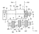
- the photoresist 95 formed over the semiconductor substrate 1 is divided into a plurality of exposure regions ER, for example, three exposure regions ER and exposure treatment is given to each of these three exposure regions ER. Accordingly, in this Embodiment, there exist two dividing lines DL for three exposure regions ER.
- a broken line 96 in FIG. 7 shows a region of the semiconductor substrate 1 in which a pixel array portion 1 is to be formed.
- FIG. 8 is a flow chart showing formation steps of the element isolation structure 3 in Step s 3 in detail.
- FIG. 8 shows a flow when the element isolation structure 3 made of a silicon oxide film is formed by an LOCOS (local oxidation of silicon) system.
- the element isolation structure 3 may be formed by an STI (shallow trench isolation) system.
- a protective film 99 having a stack structure of a silicon oxide film and a silicon nitride film is formed over the semiconductor substrate 1 in Step s 301 .
- Step s 302 a photoresist 100 is then formed over the protective film 99 .
- Step s 303 the photoresist 100 is exposed through a photomask having a predetermined mask pattern formed therein. In this step, the photoresist 100 is subjected to divided exposure.
- FIG. 9 shows the way how the divided exposure is performed in Step s 303 . As illustrated in FIG. 9 , the dividing line DL for divided exposure in the photoresist 100 is located at least over the region PAR of the semiconductor substrate 1 in which the active regions AR are to be formed.
- the dividing line DL linearly extends along the Y axis direction over a portion, of the region PAR of the semiconductor substrate 1 in which the active regions AR are to be formed, in which an N ⁇ type impurity region 11 and a source/drain region 15 of a plurality of pixels 10 belonging to a certain column are to be formed.
- the photoresist 100 is divided into three exposure regions ER. These three exposure regions ER are subjected to exposure treatment, respectively. Mask patterns corresponding to these three exposure regions ER are provided for this exposure. In other words, three mask patterns are therefore used in the exposure treatment in Step s 303 .
- FIG. 10 is a top view illustrating the photoresist 100 after patterning.
- the resist pattern of the patterned photoresist 100 is displaced in the Y axis direction between two adjacent exposure regions ER with the dividing line DL as a boundary. This occurs because misalignment occurs in the Y axis direction between two mask patterns used respectively for exposure of two adjacent exposure regions ER of the photoresist 100 .
- a step difference 101 appears on the side surface of the photoresist 100 with the dividing line DL for divided exposure as a boundary.
- Step s 305 with the photoresist 100 as a mask, the protective film 99 exposed from the photoresist 100 is etched off.
- step s 306 the photoresist 100 used as the mask is then removed.
- Step s 307 the structure thus obtained is subjected to oxidation treatment. The portion of the semiconductor substrate 1 on which the protective film 99 has been formed is not oxidized and only the portion exposed from the protective film 99 is oxidized. By this treatment, the element isolation structure 3 for defining the active regions AR is formed in the semiconductor substrate 1 . Then, the protective film 99 used as a mask is removed in Step s 308 .
- FIG. 11 is a top view illustrating the structure obtained after Step s 308 .
- a step difference 90 is formed at the periphery, in a top view, according to the step difference 101 formed on the side surface of the photoresist 100 .
- a step difference 91 is formed at the periphery, in a top view, according to the step difference 101 formed on the side surface of the photoresist 100 .
- FIG. 12 shows a flow chart illustrating a step of forming a gate structure in Step s 4 in detail.
- step s 401 as illustrated in FIG. 12 , an insulating film which will be a gate insulating film 21 is formed over the semiconductor substrate 1 .
- Step s 402 a conductive film 210 which will be as a gate electrode 20 is formed over the insulating film.
- Step s 403 a photoresist 200 is formed over the conductive film 210 .
- Step s 404 the photoresist 200 is exposed using a photomask having a predetermined mask pattern formed therein. During this exposure, the photoresist 200 is subjected to divided exposure treatment.
- FIG. 13 illustrates the way how the divided exposure treatment is performed in Step s 404 . As illustrated in FIG. 13 , a dividing line DL of the photoresist 200 for divided exposure is set at the same position as that of the dividing line DL for the divided exposure in the above-described step s 303 .
- Step s 404 the dividing line DL is located over a portion of the active regions AR in which the N ⁇ type impurity region 11 and source/drain region 15 of each of a plurality of pixels 10 of a certain column are to be formed.
- Step s 404 similar to Step s 303 , the photoresist 200 is divided into three exposure regions ER and these three exposure regions ER are subjected to exposure treatment, respectively.
- FIG. 14 is a top view illustrating the patterned photoresist 200 .
- the photoresist 200 having a shape corresponding to the shape of the gate insulating film 21 and gate electrode 20 is formed over the conductive film 210 .
- FIG. 15 is a diagram for explaining the size inspection.
- the photoresist is subjected to divided exposure treatment. Exposure treatment for a certain exposure region ER and exposure treatment for another exposure region ER are not performed simultaneously so that two or more mask patterns are used. Owing to errors upon setting exposure conditions, designing mask patterns and the like, resist patterns of the patterned photoresist which must essentially be equal sometimes are not the same between the two adjacent exposure regions ER. As a result, in the semiconductor substrate 1 , the device size sometimes differs between two regions having the dividing line DL therebetween.
- a difference in the size of the gate electrode 20 between these two regions may lead to a difference in a charge transfer ability of a transfer transistor TX or a readout speed of data from the pixel 10 between these two regions. Further, it causes a difference in the coupling capacitance between the gate electrode 20 and floating diffusion FD, resulting in difference in pixel properties and causing deterioration in image quality. Accordingly, in the photoresist subjected to divided exposure, it is very important to manage the size of the resist patterns of each of two adjacent exposure regions ER.
- Step s 406 as illustrated in FIG. 15 , the size of a resist pattern at a predetermined position 251 of one of two exposure regions ER having a dividing line DL therebetween and the size of a resist pattern at a predetermined position 252 of the other one of the two exposure regions ER are measured and these two sizes are compared.
- Step s 406 the size of the resist pattern corresponding to the shape of the gate electrode 20 in each of the two adjacent exposure regions ER is measured.
- there are two dividing lines DL so that two exposure regions ER having one of these dividing lines DL sandwiched therebetween and two exposure regions ER having the other one of these two dividing lines DL sandwiched therebetween are subjected to size inspection, respectively.
- the predetermined positions 250 and 251 are positions set as near as possible to the boundary line DL.
- Step s 406 in each of exposure regions ER of the patterned photoresist 200 , the size of the resist pattern at the predetermined position 250 at the center of the ER and the size of the resist pattern at the predetermined position 251 near the dividing line DL are measured and two sizes thus measured are compared.
- the photoresist 200 is divided into three exposure regions ER so that the size of a resist pattern is inspected in the above-described manner for each of the three exposure regions ER.
- the size measurement of the resist pattern in Step s 406 is performed using, for example, a scanning electron microscope (SEM).
- SEM scanning electron microscope
- the position of the dividing line DL is found by detecting the step differences 90 and 91 formed in the active regions AR via a scanning electron microscope.
- the step differences 90 and 91 are formed according to the positions of the dividing lines DL for divided exposure so that detection of the step differences 90 and 91 facilitate finding of the position of the dividing line DL.
- an insulating film which will be the gate insulating film 21 and a conductive film 210 which will be the gate electrode 20 are formed. These films are relatively thin so that the step differences 90 and 91 in the active regions AR can be detected using a scanning electron microscope.
- the height of the step differences 90 and 91 is preferably 0.03 ⁇ m or greater in order to detect the step differences 90 and 91 via a scanning electron microscope.
- the performance of the solid-state sensor may deteriorate when the step differences 90 and 91 are excessively high so that the height of the step differences 90 and 91 is desirably 0.3 ⁇ m or less.
- Step s 407 based on the comparison results of the size of the resist pattern in Step s 406 , the resist pattern formed in the photoresist 200 is judged whether it passes or fails the size inspection. In other words, the patterned photoresist 200 is judged whether it is as designed or not.
- Step s 407 When the resist pattern is determined to pass the size inspection in Step s 407 , the conductive film 210 and then, the insulating film therebelow exposed from the photoresist 200 are etched off successively by using the photoresist 200 as a mask in Step s 408 .
- Step s 409 the photoresist 200 used as the mask is removed, whereby, as illustrated in FIG. 16 , the gate electrodes 20 and gate insulating film 21 of the transfer transistor TX, reset transistor RST, amplified MOS imager transistor AMI, and select transistor SEL are formed.
- Step s 410 the size inspection of the gate electrode 20 which has been completed is performed.
- gate electrodes 20 of two regions having a dividing line DL therebetween which must essentially be equal in size are sometimes different on the semiconductor substrate 1 .
- Step s 410 in a region, over the semiconductor substrate 1 , in which the gate electrode 20 is formed, the gate electrode 20 of one of two partial regions corresponding to two exposure regions having a dividing line DL therebetween and the gate electrode 20 of the other partial region are measured for their sizes and two sizes thus measured are compared.
- the gate electrode 20 which must essentially be uniform in size may also differ in size between a center portion and a portion near the dividing line DL in a partial region corresponding to one of exposure regions ER in the region, over the semiconductor substrate 1 , in which the gate electrode 20 is formed.
- Step s 410 in the partial region corresponding to one of exposure regions ER in the region, over the semiconductor substrate 1 , in which the gate electrode 20 is formed, the size of the gate electrode 20 at the center portion and the size of the gate electrode 20 at a position near the dividing line DL are measured and these two sizes thus measured are compared.
- the photoresist 200 is divided into three exposure regions ER, such size inspection of the gate electrode 20 is performed in each of three partial regions corresponding to three exposure regions ER in the region, over the semiconductor substrate 1 , in which the gate electrode 20 is formed.
- Step s 410 are taken into consideration when exposure conditions in manufacturing a solid-state sensor of the next lot are determined. In other words, when the solid-state sensor of the next lot is manufactured, exposure conditions are adjusted so as to minimize the difference in the size of the gate electrode 20 .
- Step s 407 When it is determined in Step s 407 that the resist pattern fails the size inspection, the patterned photoresist 200 is removed in Step s 411 and a new photoresist 200 is formed over the conductive film 210 in step s 412 .
- Step s 413 based on the comparison results of the size of the resist pattern in Step s 406 , exposure conditions for the new photoresist 200 are adjusted.
- Step s 413 the difference in the size of the resist pattern is minimized, for example, by adjusting the exposure energy. Then, the step s 404 is performed again under thus adjusted exposure conditions, followed by similar treatment.
- FIG. 17 is a flow chart showing, in detail, the step of forming various impurity regions in Step s 5 .
- a step of forming the N ⁇ type impurity region 11 will next be described as a typical example.
- a photoresist 300 is formed over the semiconductor substrate 1 in Step s 501 .
- the photoresist 300 is exposed using a photomask having a predetermined mask pattern formed therein.
- the photoresist 300 is subjected to divided exposure treatment.
- FIG. 18 illustrates the way how the divided exposure treatment is performed in Step s 502 .
- a dividing line DL for divided exposure in the photoresist 300 is set at the same position as that of the dividing line DL for divided exposure in the above-described Steps s 303 and s 304 .
- Step s 502 the dividing line DL is located over regions, of active regions AR, in which an N ⁇ type impurity region 11 and source/drain region 15 of a plurality of pixels 10 of a certain column are to be formed.
- the photoresist 300 is divided into three exposure regions ER as in Steps s 303 and s 404 , and each of these three exposure regions is subjected to exposure treatment.
- FIG. 19 is a top view illustrating the patterned photoresist 300 .
- the photoresist 300 having an opening portion 300 a for exposing therefrom some partial active regions AR 1 is formed over the semiconductor substrate 1 .
- Step s 504 the size inspection of the resist pattern formed in Step s 503 is performed as in the above-described Step s 406 .
- the size of the opening portion 300 a formed in the photoresist 300 is measured.
- the position of a dividing line DL is confirmed by detecting step differences 90 and 91 formed in the active regions AR as in Step s 406 .
- Step s 505 based on the comparison results of the size of the resist pattern in Step s 504 , it is determined whether the size of the resist pattern formed in the photoresist 300 passes or fails the size inspection.
- an N type impurity is introduced, with the photoresist 300 as a mask, into the partial active region AR 1 exposed from the photoresist 300 by using, for example, ion implantation.
- Step s 507 the photoresist 300 used as the mask is removed.
- the N ⁇ type impurity region 11 is formed in the partial active region AR 1 of the active regions AR.
- Step s 505 When the resist pattern does not pass the size inspection in Step s 505 , on the other hand, the patterned photoresist 300 is removed in Step s 508 and a new photoresist 300 is formed over the semiconductor substrate 1 in Step s 509 .
- Step s 510 based on the comparison results of the size of the resist pattern in step s 505 , exposure conditions are adjusted for the new photoresist 300 .
- Step s 510 for example exposure energy is adjusted.
- Step s 502 is performed again under the thus adjusted exposure conditions, followed by similar treatments as described above.
- the N + type impurity region 12 , source/drain regions 13 to 16 , and P + type impurity region 17 are formed by similar treatments.
- FIG. 21 is a flow chart showing a formation step of a contact plug 40 in Step s 7 and formation step of a via plug in Step s 10 in detail.
- the contact plug and via plug are formed in a similar manner so that the formation step of the contact plug 40 will next be described as a typical example.
- Step s 701 a photoresist 400 is formed over the interlayer dielectric film 30 formed in Step s 6 .
- the photoresist 400 is exposed using a photomask having a predetermined mask pattern formed therein.
- the photoresist 400 is subjected to divided exposure treatment.
- FIG. 22 illustrates the way how the divided exposure treatment is performed in Step s 702 .
- a dividing line DL for divided exposure in the photoresist 400 is set at the same position as that of the dividing line DL for divided exposure in the above-described Steps s 303 , s 404 and s 502 .
- Step s 702 the photoresist 400 is divided into three exposure regions ER as in Steps s 303 , s 404 and s 502 , and each of the three exposure regions ER is subjected to exposure treatment.
- Step s 703 the photoresist 400 after exposure is developed and the resulting photoresist 400 is then, patterned.
- step s 704 the interlayer dielectric film 30 exposed from the photoresist 400 is etched off with the photoresist 400 as a mask. Then, the photoresist 400 used as the mask is removed in Step s 705 . As a result, a plurality of contact holes from which the N + type impurity region 12 and the like are exposed are formed in the interlayer dielectric film 30 .
- the via plug is formed in the interlayer dielectric film 60 , a via hole from which the interconnect 50 is exposed is formed in the interlayer dielectric film 60 .
- a conductive film to be filled in the contact holes in the interlayer dielectric film 30 is formed.
- a plurality of the contact plugs 40 are thus formed in the interlayer dielectric film 30 .
- a conductive film is filled in the via hole formed in the interlayer dielectric film 60 .
- FIG. 23 is a flow chart specifically showing the formation step of the lower interconnect 50 in Step s 8 and the formation step of the upper interconnect 80 in Step s 11 .
- the interconnects 50 and 80 are formed similarly so that the formation step of the interconnect 80 will next be described as a typical example.
- Step s 801 as illustrated in FIG. 23 , a conductive film 510 which will be the interconnect 80 is formed over the interlayer dielectric film 60 .
- Step s 802 a photoresist 500 is then formed over the conductive film 510 .
- Step s 803 the photoresist 500 is exposed using a photomask having a predetermined mask pattern formed therein. During exposure, the photoresist 500 is subjected to divided exposure treatment.
- FIG. 24 shows the way how the divided exposure treatment is performed in Step s 803 . As illustrated in FIG. 24 , a dividing line DL for divided exposure in the photoresist 500 is set at the same position as that of the dividing line DL in the above-described steps s 303 , s 404 , s 502 and s 702 .
- Step s 803 similar to Steps s 303 , s 404 , s 502 and s 702 , the photoresist 500 is divided into three exposure regions ER and exposure treatment is given to each of these three exposure regions ER.
- FIG. 25 is a top view illustrating the patterned photoresist 500 .
- the photoresist 500 from which an upper portion of the N ⁇ type impurity region 11 in the conductive film 410 is exposed is formed over the conductive film 510 .
- the resist patterns are displaced in the Y axis direction between two adjacent exposure regions ER with the dividing line DL as a boundary. This occurs because when two adjacent exposure regions ER in the photoresist 500 are exposed, there occurs a misalignment in the Y axis direction between two mask patterns to be used. As a result, there appears a step difference 501 on the inner side surface of the photoresist 500 with the dividing line DL for divided exposure as a boundary.
- Step s 805 with the photoresist as a mask, the conductive film 510 exposed from the photoresist 500 is etched off.
- Step s 806 the photoresist 500 used as the mask is then removed.
- the interconnect 80 is formed over the interlayer dielectric film 60 .
- a step difference 92 is formed on the inner side surface of the lattice-shaped interconnect 80 according to the step difference 501 formed in the photoresist 500
- the dividing line DL for divided exposure of the photoresist 100 to be used for defining the active regions AR in the semiconductor substrate 1 is located at least over the region PAR of the semiconductor substrate 1 in which the active regions AR are defined.
- the size of the element isolation structure 3 formed below the dividing line DL may become smaller than the original size of it owing to misalignment of two mask patterns to be used for exposure of two exposure regions ER having the dividing line DL therebetween, respectively.
- Such an element isolation structure 3 cannot fully ensure the electrical insulation properties between elements, which may cause deterioration in the performance of the solid-state sensor of this Embodiment or malfunction.
- solid-state image sensors have been required to have a large number of pixels so that a plurality of pixels 10 are densely arranged on them. This leads to a reduction in the size of the element isolation structure 3 .
- the deterioration in the performance of the solid-state image sensor due to a size change in the element isolation structure 3 has become a prominent problem.
- the dividing line DL is located only over a region in which the element isolation structure 3 present between two adjacent pixels 10 is to be formed, the original distance between pixels 10 cannot be maintained and crosstalk between the pixels 10 poses a significant problem. This results in drastic deterioration in the imaging performance of the solid-state sensor.
- the dividing line of two adjacent exposure regions ER in the photoresist 100 is located not only over a region of the semiconductor substrate 1 in which the element isolation structure 3 is to be formed but also over a region of the semiconductor substrate 1 in which active regions AR are to be formed.
- misalignment in the two mask patterns used for the exposure of these two exposure regions ER occurs, a portion of the element isolation structure 3 which undergoes a change can be minimized. This results in suppression of deterioration in the performance of the solid-state sensor. From another viewpoint, it is possible to increase a permissible misalignment amount of the mask pattern, leading to an improvement in the throughput or margin in the manufacture.
- the dividing line for divided exposure of the photoresist 100 is located over, in a region PAR of the semiconductor substrate 1 in which active regions AR are to be formed, a region in which the N ⁇ type impurity region 11 serving as a constituent element of a photodiode PD is to be formed, that is, a region in which a partial active region AR 1 is to be formed.
- the surface area of the partial active region AR 1 in which the N ⁇ type impurity region 11 is to be formed can be increased over another partial active region of the active regions AR so that even a change in the size of the partial active region AR 1 due to the misalignment of the mask pattern does not have a significant influence on the performance of the solid-state sensor. It is therefore possible to suppress deterioration in the performance of the present solid-state sensor further.
- the dividing line DL for divided exposure of the photoresist 100 is not located over, in a region PAR of the semiconductor substrate 1 in which the active regions AR are to be formed, a region in which the N + type impurity region 12 functioning as a floating diffusion FD is to be formed, that is, a region in which a partial active region AR 5 is to be formed. Even misalignment in the mask pattern therefore does not lead to a change in the size of the partial active region AR 5 . As a result, a size change of the N + type impurity region 12 can be suppressed.
- a size change of the N + type impurity region 12 occurs, a capacitance of charges accumulated in the floating diffusion FD changes, which may result in a change in the properties of a pixel corresponding to the pixel 10 having the N + type impurity region 12 . This causes deterioration in the image quality.
- a size change of the N + type impurity region 12 due to misalignment of the mask pattern can be suppressed so that deterioration in the image quality can be prevented.
- the step differences 90 and 91 are formed at the periphery, in a top view, of the active regions AR according to the position of the dividing line DL so that the position of the dividing line DL can be grasped easily by detecting the step differences 90 and 91 .
- This facilitates size measurement of the resist pattern or size measurement of the formed device based on the dividing line DL and the results of the size measurement can be fed back to exposure conditions readily.
- the step difference 92 is also formed on the side surface of the interconnect 80 according to the position of the dividing line DL.
- the position of the dividing line DL can easily be found by detecting the step difference 92 .
- the dividing line DL for divided exposure treatment when the active regions AR are defined in the semiconductor substrate 1 extends, as illustrated in FIG. 9 , along the Y axis direction over a region of the semiconductor substrate 1 in which the partial active region AR 1 is to be formed.
- the dividing line DL extends over the region of the semiconductor substrate 1 in which the partial active region AR 1 is to be formed and along the shorter direction of the region.
- FIG. 27 shows it.
- a region 700 in FIG. 27 shows the variation amount of the surface area of the partial active region AR 1 when the dividing line DL extends along the shorter direction of the region of the semiconductor substrate 1 in which the partial active region AR 1 is to be formed.
- a region 701 in FIG. 27 shows the variation amount of the surface area of the partial active region AR 1 when the dividing line DL extends along the longer direction of the region of the semiconductor substrate 1 in which the partial active region AR 1 is to be formed.
- the dividing line DL for divided exposure treatment in defining the active regions AR in the semiconductor substrate 1 extends along the longer direction of the region of the semiconductor substrate 1 in which the partial active region AR 1 is to be formed, a variation amount of the surface area of the partial active region AR 1 due to misalignment of the mask pattern increases. Since the N ⁇ type impurity region 11 of the photodiode PD is formed in the partial active region AR 1 , a variation in the surface area of the partial active region AR 1 leads to a variation in the surface area of the N ⁇ type impurity region 11 and also a variation in the sensitivity of photoelectric conversion in the photodiode PD. As a result, deterioration in the image quality occurs.
- the dividing line DL for the divided exposure treatment in defining the active regions AR in the semiconductor substrate 1 extends along the shorter direction of the region of the semiconductor substrate 1 in which the partial active region AR 1 is to be formed, a variation in the surface area of the partial active region AR 1 can be suppressed, leading to prevention of deterioration in the image quality.
- the dividing line DL for divided exposure treatment in defining the active regions AR in the semiconductor substrate 1 is not located over regions of the semiconductor substrate 1 in which partial active regions AR 2 to AR 4 , AR 6 and AR 7 , among a plurality of partial active regions AR 1 to AR 7 , to be brought into contact with the contact plug 40 are formed.
- a step difference similar to the step difference 91 of the partial active region AR 5 appears at the periphery of the partial active region AR 2 owing to misalignment of the mask pattern upon divided exposure and it reduces the distance between the element isolation structure 3 around the partial active region AR 2 and the contact plug 40 . This may increase the leakage current between the contact plug 40 and the well region 2 .
- the gate electrode 20 used for the latter step is aligned with the active region AR to be formed in the former step so that the mask pattern of a photomask used for the formation of the gate electrode 20 is designed based on a mask pattern of a photomask to be used for defining the active regions AR in the semiconductor substrate 1 .
- the contact plug 40 is aligned with the gate electrode 20 so that a mask pattern of a photomask to be used for the formation of the contact plug 40 is designed based on a mask pattern of a photomask to be used for the formation of the gate electrode 20 .
- the lower interconnect 50 is aligned with the contact plug 40 so that a mask pattern of a photomask to be used for the formation of the interconnect 50 is designed based on a mask pattern of a photomask to be used for the formation of the contact plug 40 .
- the via plug is aligned with the interconnect 50 so that a mask pattern of a photomask to be used for the formation of the via plug is designed based on a mask pattern of a photomask to be used for the formation of the interconnect 50 .
- the upper interconnect 80 is aligned with the via plug so that a mask pattern of a photomask to be used for the formation of the interconnect 80 is designed based on a mask pattern of a photomask to be used for the formation of the via plug.
- dividing lines DL for divided exposure are preferably set at the same position.
- dividing lines DL for divided exposure for defining the active regions AR in the semiconductor substrate 1 and for forming the gate electrode 20 are preferably set at the same position.
- the dividing lines for divided exposure are set at different positions, deterioration in alignment accuracy due to misalignment of the mask pattern may reduce the yield.
- a dividing line DLA which is a dividing line DL for the formation of the gate electrode 20
- a dividing line DLB which is a dividing line DL for the formation of the contact plug 40
- the distance between the gate electrode 20 of the amplified MOS imager transistor AMI and the contact plug 40 over the partial active region AR 4 may become a permissible distance or less and a reduction in the yield may occur when a mask pattern to be used for exposure of an exposure region ER
- the dividing line DL for divided exposure treatment for forming the N ⁇ type impurity region 11 in the semiconductor substrate 1 is preferably located not over the partial active region AR 1 as illustrated in FIG. 29 .
- misalignment of the mask pattern during divided exposure causes a change in the shape of the opening portion 300 a of the photoresist 300 and a change in the shape of the N ⁇ type impurity region 11 , which may result in a drastic change in the sensitivity of photoelectric conversion in the photodiode PD. This deteriorates the image quality.
- the dividing lines DL for forming the N ⁇ type impurity region 11 , N + type impurity region 12 , source/drain regions 13 to 16 and P + type impurity region 17 are located at predetermined positions so that photomasks can be designed more easily.
- the dividing line is located over the partial active region AR 7 so that the shape of the P + type impurity region 17 may change due to misalignment of the mask pattern upon divided exposure. Since the P + type impurity region 17 is an impurity region to which a ground potential GND, a negative-side power supply potential, is applied, even a change in the shape of the P + type impurity region 17 does not lead to a substantial change in the properties of the pixel 10 .
- the active regions AR having the pixels 10 formed therein include partial active regions AR 1 and AR 5 having step differences 90 and 91 , respectively, at the periphery in a top view so that when the photoresist 100 to be used for defining the active regions AR in the semiconductor substrate 1 is subjected to divided exposure with the positions of the step differences 90 and 91 of the partial active regions AR 1 and AR 5 as a boundary, the positions of the dividing lines DL for divided exposure can be found easily by detecting the step differences 90 and 91 .
- the interconnect 80 has, on the side surface thereof, the step difference 92 .
- the interconnect 80 is formed, divided exposure is performed with the position of the difference 92 as a boundary, the dividing line DL for divided exposure can be found readily by detecting the step difference 92 .
- the contact plugs 40 are not contiguous onto the partial active regions AR 1 and AR 5 having at the periphery thereof step differences 90 and 91 , respectively, an increase in the leakage current between the contact plug 40 and well region 2 can be inhibited.
Landscapes
- Solid State Image Pick-Up Elements (AREA)
- Exposure And Positioning Against Photoresist Photosensitive Materials (AREA)
- Exposure Of Semiconductors, Excluding Electron Or Ion Beam Exposure (AREA)
Abstract
Description
Claims (12)
Priority Applications (1)
| Application Number | Priority Date | Filing Date | Title |
|---|---|---|---|
| US12/773,171 US8030693B2 (en) | 2007-04-12 | 2010-05-04 | Solid-state image sensor |
Applications Claiming Priority (2)
| Application Number | Priority Date | Filing Date | Title |
|---|---|---|---|
| JP2007104554A JP5214904B2 (en) | 2007-04-12 | 2007-04-12 | Manufacturing method of solid-state imaging device |
| JP2007-104554 | 2007-04-12 |
Related Child Applications (1)
| Application Number | Title | Priority Date | Filing Date |
|---|---|---|---|
| US12/773,171 Division US8030693B2 (en) | 2007-04-12 | 2010-05-04 | Solid-state image sensor |
Publications (2)
| Publication Number | Publication Date |
|---|---|
| US20080254564A1 US20080254564A1 (en) | 2008-10-16 |
| US7732239B2 true US7732239B2 (en) | 2010-06-08 |
Family
ID=39854080
Family Applications (2)
| Application Number | Title | Priority Date | Filing Date |
|---|---|---|---|
| US12/050,930 Active 2028-04-01 US7732239B2 (en) | 2007-04-12 | 2008-03-18 | Method for manufacturing solid-state image sensor |
| US12/773,171 Active US8030693B2 (en) | 2007-04-12 | 2010-05-04 | Solid-state image sensor |
Family Applications After (1)
| Application Number | Title | Priority Date | Filing Date |
|---|---|---|---|
| US12/773,171 Active US8030693B2 (en) | 2007-04-12 | 2010-05-04 | Solid-state image sensor |
Country Status (2)
| Country | Link |
|---|---|
| US (2) | US7732239B2 (en) |
| JP (1) | JP5214904B2 (en) |
Cited By (3)
| Publication number | Priority date | Publication date | Assignee | Title |
|---|---|---|---|---|
| US20160284759A1 (en) * | 2015-03-27 | 2016-09-29 | Renesas Electronics Corporation | Semiconductor device |
| US9515117B2 (en) | 2014-06-05 | 2016-12-06 | Renesas Electronics Corporation | Method of manufacturing an image sensor using multiple exposures |
| US20170077165A1 (en) * | 2015-09-10 | 2017-03-16 | Renesas Electronics Corporation | Method of manufacturing semiconductor unit and the semiconductor unit |
Families Citing this family (9)
| Publication number | Priority date | Publication date | Assignee | Title |
|---|---|---|---|---|
| JP5487734B2 (en) * | 2009-06-05 | 2014-05-07 | 株式会社ニコン | Solid-state image sensor |
| JP2016178345A (en) * | 2010-11-16 | 2016-10-06 | キヤノン株式会社 | Solid-state imaging device, method for manufacturing solid-state imaging device, and imaging system |
| JP5986399B2 (en) * | 2012-02-29 | 2016-09-06 | キヤノン株式会社 | Manufacturing method of semiconductor device |
| JP2013182943A (en) * | 2012-02-29 | 2013-09-12 | Canon Inc | Method of manufacturing solid state imaging device |
| US8686477B2 (en) * | 2012-07-25 | 2014-04-01 | Omnivision Technologies, Inc. | Ground contact structure for a low dark current CMOS pixel cell |
| JP2014090088A (en) * | 2012-10-30 | 2014-05-15 | Renesas Electronics Corp | Semiconductor device and manufacturing method of the same |
| JP6110154B2 (en) * | 2013-02-13 | 2017-04-05 | 浜松ホトニクス株式会社 | Solid-state imaging device and method for manufacturing solid-state imaging device |
| JP5886793B2 (en) * | 2013-06-11 | 2016-03-16 | 浜松ホトニクス株式会社 | Solid-state imaging device |
| TWI701819B (en) * | 2015-06-09 | 2020-08-11 | 日商索尼半導體解決方案公司 | Imaging element, driving method and electronic equipment |
Citations (10)
| Publication number | Priority date | Publication date | Assignee | Title |
|---|---|---|---|---|
| JPH056849A (en) | 1990-08-24 | 1993-01-14 | Canon Inc | Method for manufacturing semiconductor device |
| JPH0562874A (en) | 1991-09-05 | 1993-03-12 | Fujitsu Ltd | Method for manufacturing semiconductor device |
| JPH06124869A (en) | 1992-10-13 | 1994-05-06 | Sharp Corp | Manufacture of semiconductor device |
| US5561317A (en) | 1990-08-24 | 1996-10-01 | Canon Kabushiki Kaisha | Method of manufacturing semiconductor devices |
| JPH09190962A (en) | 1996-01-10 | 1997-07-22 | Nikon Corp | Semiconductor device, reticle, and projection exposure method |
| JPH09298155A (en) | 1996-05-08 | 1997-11-18 | Nikon Corp | Exposure method, exposure apparatus, and mask |
| JPH11220116A (en) | 1998-01-30 | 1999-08-10 | Nikon Corp | Semiconductor device and manufacturing method thereof |
| US6204912B1 (en) | 1996-05-08 | 2001-03-20 | Nikon Corporation | Exposure method, exposure apparatus, and mask |
| JP2003005346A (en) | 2001-06-21 | 2003-01-08 | Toshiba Corp | Mask manufacturing method and mask manufacturing apparatus |
| US7413921B2 (en) * | 2005-06-10 | 2008-08-19 | Samsung Electronics Co., Ltd. | Method of manufacturing image sensor |
Family Cites Families (4)
| Publication number | Priority date | Publication date | Assignee | Title |
|---|---|---|---|---|
| JP2720441B2 (en) * | 1988-01-21 | 1998-03-04 | ソニー株式会社 | Pattern formation method for charge transfer device |
| JP2004111866A (en) * | 2002-09-20 | 2004-04-08 | Canon Inc | Semiconductor device manufacturing method |
| US7541628B2 (en) * | 2005-07-09 | 2009-06-02 | Samsung Electronics Co., Ltd. | Image sensors including active pixel sensor arrays |
| KR100731120B1 (en) * | 2005-12-28 | 2007-06-22 | 동부일렉트로닉스 주식회사 | CMOS image sensor and its manufacturing method |
-
2007
- 2007-04-12 JP JP2007104554A patent/JP5214904B2/en active Active
-
2008
- 2008-03-18 US US12/050,930 patent/US7732239B2/en active Active
-
2010
- 2010-05-04 US US12/773,171 patent/US8030693B2/en active Active
Patent Citations (12)
| Publication number | Priority date | Publication date | Assignee | Title |
|---|---|---|---|---|
| JPH056849A (en) | 1990-08-24 | 1993-01-14 | Canon Inc | Method for manufacturing semiconductor device |
| US5561317A (en) | 1990-08-24 | 1996-10-01 | Canon Kabushiki Kaisha | Method of manufacturing semiconductor devices |
| JPH0562874A (en) | 1991-09-05 | 1993-03-12 | Fujitsu Ltd | Method for manufacturing semiconductor device |
| JPH06124869A (en) | 1992-10-13 | 1994-05-06 | Sharp Corp | Manufacture of semiconductor device |
| US5451488A (en) | 1992-10-13 | 1995-09-19 | Sharp Kabushiki Kaisha | Reticle having sub-patterns and a method of exposure using the same |
| JPH09190962A (en) | 1996-01-10 | 1997-07-22 | Nikon Corp | Semiconductor device, reticle, and projection exposure method |
| US5888676A (en) | 1996-01-10 | 1999-03-30 | Nikon Corporation | Projection-exposure method for manufacturing semiconductor device and devices made using same |
| JPH09298155A (en) | 1996-05-08 | 1997-11-18 | Nikon Corp | Exposure method, exposure apparatus, and mask |
| US6204912B1 (en) | 1996-05-08 | 2001-03-20 | Nikon Corporation | Exposure method, exposure apparatus, and mask |
| JPH11220116A (en) | 1998-01-30 | 1999-08-10 | Nikon Corp | Semiconductor device and manufacturing method thereof |
| JP2003005346A (en) | 2001-06-21 | 2003-01-08 | Toshiba Corp | Mask manufacturing method and mask manufacturing apparatus |
| US7413921B2 (en) * | 2005-06-10 | 2008-08-19 | Samsung Electronics Co., Ltd. | Method of manufacturing image sensor |
Cited By (10)
| Publication number | Priority date | Publication date | Assignee | Title |
|---|---|---|---|---|
| US9515117B2 (en) | 2014-06-05 | 2016-12-06 | Renesas Electronics Corporation | Method of manufacturing an image sensor using multiple exposures |
| US20170077153A1 (en) * | 2014-06-05 | 2017-03-16 | Renesas Electronics Corporation | Manufacturing method of semiconductor device and semiconductor device |
| US9704906B2 (en) * | 2014-06-05 | 2017-07-11 | Renesas Electronics Corporation | Manufacturing method of semiconductor device and semiconductor device |
| US20160284759A1 (en) * | 2015-03-27 | 2016-09-29 | Renesas Electronics Corporation | Semiconductor device |
| US9761625B2 (en) * | 2015-03-27 | 2017-09-12 | Renesas Electronics Corporation | Image sensor having overlapping exposure regions and pixels with misaligned photodiodes |
| US9893109B2 (en) | 2015-03-27 | 2018-02-13 | Renesas Electronics Corporation | Method for manufacturing a solid state image sensor with pixels having photodiodes patterned through overlapping divided exposure |
| US20170077165A1 (en) * | 2015-09-10 | 2017-03-16 | Renesas Electronics Corporation | Method of manufacturing semiconductor unit and the semiconductor unit |
| US9793311B2 (en) * | 2015-09-10 | 2017-10-17 | Renesas Electronics Corporation | Method of manufacturing semiconductor unit and the semiconductor unit |
| US20170373112A1 (en) * | 2015-09-10 | 2017-12-28 | Renesas Electronics Corporation | Method of manufacturing semiconductor unit and the semiconductor unit |
| US10074686B2 (en) * | 2015-09-10 | 2018-09-11 | Renesas Electronics Corporation | Method of manufacturing semiconductor unit and the semiconductor unit |
Also Published As
| Publication number | Publication date |
|---|---|
| JP2008263050A (en) | 2008-10-30 |
| JP5214904B2 (en) | 2013-06-19 |
| US8030693B2 (en) | 2011-10-04 |
| US20100213567A1 (en) | 2010-08-26 |
| US20080254564A1 (en) | 2008-10-16 |
Similar Documents
| Publication | Publication Date | Title |
|---|---|---|
| US7732239B2 (en) | Method for manufacturing solid-state image sensor | |
| US20210098515A1 (en) | Solid-state image pickup device | |
| US6486521B2 (en) | Optimized floating P+ region photodiode for a CMOS image sensor | |
| US10825849B2 (en) | Solid-state image pickup device | |
| KR101683297B1 (en) | Solid-state imaging device, solid-state imaging device manufacturing method, elelctronic device, and lens array | |
| JP5487798B2 (en) | Solid-state imaging device, electronic apparatus, and manufacturing method of solid-state imaging device | |
| KR100881200B1 (en) | CMOS image sensor and its manufacturing method | |
| US7372491B2 (en) | CMOS image sensor | |
| CN105390445A (en) | Semiconductor device manufacturing method and semiconductor device | |
| US8980540B2 (en) | Method of manufacturing solid-state image sensor | |
| KR100606902B1 (en) | Manufacturing Method of CMOS Image Sensor | |
| US20230245977A1 (en) | Alignment Method for Image Sensor Fabrication and Associated Semiconductor Device | |
| JP5855695B2 (en) | Solid-state image sensor manufacturing method and solid-state image sensor | |
| KR100514110B1 (en) | Solid-state image sensor and manufacturing method therefor | |
| US7135362B2 (en) | Isolation layer for CMOS image sensor and fabrication method thereof | |
| US20050285166A1 (en) | Monitoring patterns for an imaging device and method of monitoring a process using the monitoring patterns | |
| JP5768073B2 (en) | Solid-state image sensor manufacturing method and solid-state image sensor | |
| US20220013562A1 (en) | Image sensing device | |
| KR19990058633A (en) | Photodiode Formation Method of Solid State Imaging Device | |
| JPH04257265A (en) | Manufacture of solid-state image sensing device | |
| JPH05315589A (en) | Solid-state image sensor | |
| KR20080062140A (en) | CMOS image sensor and its manufacturing method |
Legal Events
| Date | Code | Title | Description |
|---|---|---|---|
| AS | Assignment |
Owner name: RENESAS TECHNOLOGY CORP., JAPAN Free format text: ASSIGNMENT OF ASSIGNORS INTEREST;ASSIGNORS:KIMURA, MASATOSHI;HONDA, HIROKI;REEL/FRAME:020674/0096 Effective date: 20080212 Owner name: RENESAS TECHNOLOGY CORP.,JAPAN Free format text: ASSIGNMENT OF ASSIGNORS INTEREST;ASSIGNORS:KIMURA, MASATOSHI;HONDA, HIROKI;REEL/FRAME:020674/0096 Effective date: 20080212 |
|
| STCF | Information on status: patent grant |
Free format text: PATENTED CASE |
|
| AS | Assignment |
Owner name: RENESAS ELECTRONICS CORPORATION, JAPAN Free format text: CHANGE OF NAME;ASSIGNOR:NEC ELECTRONICS CORPORATION;REEL/FRAME:024864/0635 Effective date: 20100401 Owner name: NEC ELECTRONICS CORPORATION, JAPAN Free format text: MERGER;ASSIGNOR:RENESAS TECHNOLOGY CORP.;REEL/FRAME:024879/0190 Effective date: 20100401 |
|
| FEPP | Fee payment procedure |
Free format text: PAYOR NUMBER ASSIGNED (ORIGINAL EVENT CODE: ASPN); ENTITY STATUS OF PATENT OWNER: LARGE ENTITY |
|
| FPAY | Fee payment |
Year of fee payment: 4 |
|
| MAFP | Maintenance fee payment |
Free format text: PAYMENT OF MAINTENANCE FEE, 8TH YEAR, LARGE ENTITY (ORIGINAL EVENT CODE: M1552) Year of fee payment: 8 |
|
| AS | Assignment |
Owner name: RENESAS ELECTRONICS CORPORATION, JAPAN Free format text: CHANGE OF ADDRESS;ASSIGNOR:RENESAS ELECTRONICS CORPORATION;REEL/FRAME:044928/0001 Effective date: 20150806 |
|
| MAFP | Maintenance fee payment |
Free format text: PAYMENT OF MAINTENANCE FEE, 12TH YEAR, LARGE ENTITY (ORIGINAL EVENT CODE: M1553); ENTITY STATUS OF PATENT OWNER: LARGE ENTITY Year of fee payment: 12 |