US7719031B2 - Heterojunction biploar transistor and method for manufacturing same - Google Patents
Heterojunction biploar transistor and method for manufacturing same Download PDFInfo
- Publication number
- US7719031B2 US7719031B2 US10/564,085 US56408504A US7719031B2 US 7719031 B2 US7719031 B2 US 7719031B2 US 56408504 A US56408504 A US 56408504A US 7719031 B2 US7719031 B2 US 7719031B2
- Authority
- US
- United States
- Prior art keywords
- layer
- silicon
- extrinsic base
- sige
- region
- Prior art date
- Legal status (The legal status is an assumption and is not a legal conclusion. Google has not performed a legal analysis and makes no representation as to the accuracy of the status listed.)
- Expired - Fee Related, expires
Links
Images


Classifications
-
- H—ELECTRICITY
- H10—SEMICONDUCTOR DEVICES; ELECTRIC SOLID-STATE DEVICES NOT OTHERWISE PROVIDED FOR
- H10D—INORGANIC ELECTRIC SEMICONDUCTOR DEVICES
- H10D10/00—Bipolar junction transistors [BJT]
- H10D10/01—Manufacture or treatment
- H10D10/021—Manufacture or treatment of heterojunction BJTs [HBT]
-
- H—ELECTRICITY
- H10—SEMICONDUCTOR DEVICES; ELECTRIC SOLID-STATE DEVICES NOT OTHERWISE PROVIDED FOR
- H10D—INORGANIC ELECTRIC SEMICONDUCTOR DEVICES
- H10D10/00—Bipolar junction transistors [BJT]
- H10D10/80—Heterojunction BJTs
- H10D10/821—Vertical heterojunction BJTs
- H10D10/891—Vertical heterojunction BJTs comprising lattice-mismatched active layers, e.g. SiGe strained-layer transistors
Definitions
- the present invention relates to a heterojunction bipolar transistor with base layers formed by epitaxial growth and a method for manufacturing the same.
- HBTs heterojunction bipolar transistors
- materials different in bandwidth are introduced to base layers using epitaxial growth to increase device speed.
- HBT with base layers using family-IV semiconductor materials such as SiGe (silicon-germanium) material and SiGeC (silicon-germanium carbon) material is highly expected as a high-speed device because the device can be formed on a Si substrate and integration with CMOS circuits and large substrate are advantageous in terms of high performance and low cost.
- SiGe HBT A typical configuration example of a conventional HBT using SiGe for heterojunction (hereinafter referred as to SiGe HBT) is explained with reference to FIG. 23 . While the HBT using SiGe material for base layers is exemplified here, a HBT using SiGeC material for the base layers is to have the same configuration.
- the SiGe HBT is generally classified into a double-polysilicon structure and a single-polysilicon structure.
- FIG. 23( a ) is a typical schematic sectional view of the SiGe HBT of the double-polysilicon structure and
- FIG. 23( b ) is that of the SiGe HBT of the single-polysilicon structure.
- a polysilicon layer 103 corresponding to an extrinsic base region is formed in advance on a Si substrate provided with an isolation area 101 and a collector region 102 . And the polysilicon layer 103 is subject to a patterning treatment by etching. An epitaxial SiGe layer 104 corresponding to an intrinsic base region selectively and epitaxially grows on an HBT formation region removed the polysilicon layer 103 .
- the polysilicon layer 103 and the epitaxial SiGe layer 104 can not be formed simultaneously or continuously. Therefore, it is difficult to avoid native oxide film formed on an interface 105 between the epitaxial SiGe layer 104 and the polysilicon layer 103 . Also, there is a possibility of generating void inside the interface 105 .
- the SiGeHBT of the double-polysilicon structure increases contact resistance between the polysilicon layer 103 and the epitaxial SiGe layer 104 and it causes a problem that uneven contact resistance exists among products. And it has further problems that manufacturing process is complicated and process window is small during selective growth. From these viewpoints, the SiGeHBT of the double-polysilicon structure is not suitable for mass production.
- an epitaxial SiGe layer 106 corresponding to the intrinsic base region epitaxially grows on the Si substrate directly above the collector region 102 .
- a polySiGe layer 107 corresponding to an extrinsic base region epitaxially grows on an isolation region 101 .
- a silicide layer 108 is formed on a surface of the polySiGe layer 107 .
- the SiGeHBT of the single-polysilicon structure is suitable for mass production.
- the epitaxial SiGe layer 106 corresponding to the intrinsic base region and the polySiGe layer 107 corresponding to the extrinsic base region are formed by the same manufacturing process simultaneously, thereby a Ge composition profile existing in the extrinsic base region is inevitably coincided with that existing in the intrinsic base region.
- the Ge composition profile optimized in the intrinsic base region is not necessarily suitable as a Ge composition profile of the extrinsic base region. Accordingly, the inventor considers the following defects occur.
- FIG. 24 shows layer structure of the base layers of the conventional SiGeHBT
- FIG. 25 shows change of the Ge composition profile contained in each layer of the base layers.
- a Si buffer layer 109 , a non-dope SiGe spacer layer 110 , a B-dope SiGe graded base layer 111 , and a Si cap layer 112 are formed in order upwardly from the Si substrate.
- These layers, 109 , 110 , 111 , 112 as a whole are represented by “the intrinsic base region 106 ” and correspond to the monocrystal epitaxial SiGe layer 106 shown in FIG. 23( b ).
- a first layer 113 as an extrinsic base formation layer (the layer formed simultaneously with the Si buffer layer 109 ), a second layer 114 formed simultaneously with the non-dope SiGe spacer layer 110 , a third layer 115 formed simultaneously with the B-dope SiGe graded base layer 111 , and a fourth layer 116 formed simultaneously with the Si cap layer 112 are formed in order upwardly from the substrate.
- These layers 113 , 114 , 115 and 116 as a whole are represented by “the extrinsic base region 107 ” and correspond to the polycrystal polySiGe layer 107 shown in FIG. 23( b ).
- the Ge composition profile of the layer structure corresponding to the intrinsic base region 106 is optimized to improve device property.
- the Si graded base layer 111 has the graded composition base structure in which Ge content gradually increases from the emitter to the collector. Thereby, an electric field is formed inside the base layer, which accelerates the carrier (electron) so as to decrease electron transit time for the base layer, and then high frequency property (high speed of the device) is obtained.
- thickness of the Si cap layer 112 of the intrinsic base region 106 is represented by a horizontal axis and the base resistance and the maximum gained frequency fmax is represented by a vertical axis.
- FIG. 26 illustrates the state of variation of measured fmax data and the base resistance for the thickness of Si cap layer 112 .
- Values of the vertical axis are relative values which are normalized and rearranged with each value in 30 nm thickness of the Si cap 112 .
- an unexpected result is that although the Si cap layer 112 is thinned and intended to speed up the device, the base resistance rapidly increases with the thickness of not less than 10 nm and then fmax largely decreases.
- the primary factor of increase of this base resistance may be that because the Si cap layer 112 of the intrinsic base region 106 and the fourth layer 116 comprising silicon of the extrinsic base region 107 are thinned, Ge atom contained in the lower third layer 115 (SiGe layer) inhibits the formation of the silicide layer so as to increase resistance of the silicide layer 108 during the silicidation of the surface of the fourth layer 116 .
- Rim et al. showed a finding that resistance of the silicide layer can be decreased by selective growth of the Si layer referred to as “raised source/drain (RDS)” on the SiGe layer immediately before the silicidation.
- RDS raised source/drain
- Jagannathan et al. have described in “IEEE Electron Device Letters Vol. 23 (2002) P. 258-260” that, in the process of manufacturing SiGe HBTs of the single-poly silicon structure, the intrinsic base region is masked and the layer referred to as “raised extrinsic base” is formed on the extrinsic base region by selective growth after the epitaxial SiGe layer corresponding to the intrinsic base region and the polySiGe layer corresponding to the extrinsic base region are formed simultaneously.
- Jagannathan et al. did not refer to the resistance of the silicide layer, they may imply that this function of “raised extrinsic base” improves inhibition of silicidation resulting from Ge atom.
- An object of the present invention is to provide a SiGe HBT of the single-poly silicon structure and a method of manufacturing the same where the silicide layer can be evenly formed in the extrinsic base region for higher speed of transistor performance, so that high silicide resistance resulting from Ge atom can be prevented securely without complicated processes of manufacturing transistors.
- a bipolar transistor of the present invention comprises a substrate; an intrinsic base region having a silicon buffer layer comprised of silicon which is formed on said substrate, and a composition-ratio graded base layer which is formed on the silicon buffer layer and comprises silicon and at least germanium and where a composition ratio of the germanium to the silicon varies in a thickness direction of the composition-ratio graded base layer; and an extrinsic base region having an extrinsic base formation layer comprised of silicon which is formed on the substrate and adjacent to the silicon buffer layer; wherein each of the extrinsic base formation layer and the silicon buffer layer has a thickness of not less than 40 nm and a surface of the extrinsic base formation layer is silicided.
- a bipolar transistor of the present invention comprises a substrate; an intrinsic base region having a silicon buffer layer comprised of silicon which is formed on said substrate, and a composition-ratio graded base layer which is formed on the silicon buffer layer and comprises silicon and at least germanium and where a composition ratio of the germanium to the silicon varies in a thickness direction of the composition-ratio graded base layer; and an extrinsic base region having an extrinsic base formation layer comprised of silicon which is formed on said substrate and adjacent to the silicon buffer layer; wherein thickness of the extrinsic base formation layer is substantially equal to a thickness of the silicon buffer layer and a surface of the extrinsic base formation layer is silicided.
- the silicide layer can be formed on the extrinsic base formation layer after the extrinsic base formation layer with a predetermined thick film has been formed, thereby the silicide layer can be evenly formed on the extrinsic base formation layer. Further, a layer containing germanium does not exist beneath the extrinsic base formation layer, so that the silicidation is not inhibited by Ge atom during the formation of silicide layer in the extrinsic base formation layer, thereby higher silicide resistance can be securely prevented.
- composition-ratio graded base layer may be a silicon germanium graded base layer which comprises silicon and germanium.
- the silicon buffer layer may be comprised of monocrystal and the extrinsic base formation layer may be comprised of polycrystal.
- a method of manufacturing a bipolar transistor of the present invention comprises a step of forming a masking layer on a substrate so as to enclose a region including an active region; a step of forming an epitaxial base layer such that the epitaxial base layer has a silicon layer and a silicon-germanium layer in the active region; a step of, non-selectively with respect to the epitaxial base layer, forming a poly-base layer such that the poly-base layer has a silicon layer and a silicon-germanium layer in an isolation region of the region including the active region; and a step of thereafter removing the silicon-germanium layer of the poly-base layer by etching process to expose a surface of the silicon layer as an extrinsic base formation layer, and a step of forming a silicide layer on the exposed surface.
- This manufacturing method employs steps where after the silicon-germanium layer has been laminated on the extrinsic base formation layer, the silicon-germanium layer is removed by etching to form the silicide layer on the extrinsic base formation layer. Thereby, silicidation is not inhibited by Ge atom in the step of forming the silicide layer on the extrinsic base formation layer and increase of silicide resistance is securely prevented.
- the etching process is preferably a wet etching which uses an etchant made of a mixture comprising nitric acid, water and fluorinated acid.
- a bipolar transistor of the present invention comprises a substrate; an intrinsic base region having a silicon buffer layer comprised of silicon which is formed on said substrate, and a composition-ratio graded base layer which is formed on the silicon buffer layer and comprises silicon and at least germanium and where a composition ratio of the germanium to the silicon varies in a thickness direction of the composition-ratio graded base layer; and an extrinsic base region having a first extrinsic base formation layer comprised of silicon which is disposed adjacent to the silicon buffer layer on the substrate; a second extrinsic base formation layer containing germanium which is formed on the first extrinsic base formation layer, together with the composition-ratio graded base layer; and a third extrinsic base layer comprised of silicon which is formed on the second extrinsic base formation layer; wherein germanium content of the second extrinsic base formation layer is lower than that of the composition-ratio graded base layer and a surface of the third extrinsic base formation layer is silicide
- This configuration makes the germanium content of the second extrinsic base formation layer lower than that of the silicon-germanium graded base layer. Thereby, it is ensured to prevent increase of silicide resistance resulting from inhibition of silicidation due to Ge atom during the step of forming the silicide layer on the silicon layer of the second extrinsic base formation layer.
- composition-ratio graded base layer may be comprised of monocrystal and the second extrinsic base formation layer may be comprised of polycrystal.
- a method of manufacturing a bipolar transistor of the present invention comprises a step of forming a masking layer on a substrate so as to enclose a region including an active region; a step of forming a first silicon layer in the active region of the region including the active region while forming a second silicon layer in an isolation region of the region including the active region by a first vapor phase growth method; and a step of thereafter forming a first silicon-germanium layer comprised of monocrystal on the first silicon layer while forming a second silicon-germanium layer comprised of polycrystal on the second silicon layer by a second chemical vapor phase growth method based on reactant gas of chlorine addition, wherein a silicide layer is formed on a surface of a third silicon layer as an extrinsic base formation layer formed on the second silicon-germanium layer.
- thickness of these layers is adjusted such that germanium content of the second silicon-germanium layer is lower than that of the first silicon-germanium layer.
- the second silicon-germanium layer comprising silicon and germanium is formed by a vapor phase growth based on reactant gas of chlorine addition; thereby growth of the extrinsic base formation layer is suppressed under etching function of the reactant gas containing chlorine.
- germanium content of the second silicon-germanium layer can be made lower than that of the first silicon-germanium layer.
- the silicide layer on the third silicon layer covering the second silicon-germanium layer it is ensured that silicidation is not affected by Ge atom so as to prevent increase of silicide resistance.
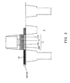
- FIG. 1 is a sectional view showing a SiGe HBT of a first embodiment in the present invention.
- FIG. 2 is a sectional view showing a base layer of the SiGe HBT of the first embodiment in the present invention.
- FIG. 3 is a sectional view showing a step of manufacturing the SiGe HBT of the first embodiment.
- FIG. 4 is a sectional view showing a step following the step of FIG. 3 for manufacturing the SiGe HBT.
- FIG. 5 is a sectional view showing a step following the step of FIG. 4 for manufacturing the SiGe HBT.
- FIG. 6 is a sectional view showing a step following the step of FIG. 5 for manufacturing the SiGe HBT.
- FIG. 7 is a sectional view showing a step following the step of FIG. 6 for manufacturing the SiGe HBT.
- FIG. 8 is a sectional view showing a step following the step of FIG. 7 for manufacturing the SiGe HBT.
- FIG. 9 is a sectional view showing a step following the step of FIG. 8 for manufacturing the SiGe HBT.
- FIG. 10 is a sectional view showing a step following the step of FIG. 9 for manufacturing the SiGe HBT.
- FIG. 11 is a sectional view showing a step following the step of FIG. 10 for manufacturing the SiGe HBT.
- FIG. 12 is a sectional view showing a step following the step of FIG. 11 for manufacturing the SiGe HBT.
- FIG. 13 is a sectional view showing a step following the step of FIG. 12 for manufacturing the SiGe HBT.
- FIG. 14 is a sectional view showing a step following the step of FIG. 13 for manufacturing the SiGe HBT.
- FIG. 15 is a sectional view showing a SiGe HBT of a second embodiment in the present invention.
- FIG. 16 is a sectional view showing a base layer of the SiGe HBT of the second embodiment in the present invention.
- FIG. 17 is a sectional view showing a step of manufacturing the SiGe HBT of the second embodiment.
- FIG. 18 is a sectional view showing a step following the step of FIG. 17 for manufacturing the SiGe HBT.
- FIG. 19 is a sectional view showing a step following the step of FIG. 18 for manufacturing the SiGe HBT.
- FIG. 20 is a sectional view showing a step following the step of FIG. 19 for manufacturing the SiGe HBT.
- FIG. 21 is a sectional view showing a step following the step of FIG. 20 for manufacturing the SiGe HBT.
- FIG. 22 is a sectional view showing a step following the step of FIG. 21 for manufacturing the SiGe HBT.
- FIG. 23 is a sectional view showing the conventional SiGe HBT.
- FIG. 24 is a sectional view showing a base layer of the SiGe HBT.
- FIG. 25 is a view showing a Ge atom composition profile of the base layer of the SiGe HBT.
- FIG. 26 is showing a data of dependence measurement of the Si cap film thickness with regard to the base resistance and fmax in the conventional SiGe HBT.
- FIG. 27 is schematically showing SEM sectional pictures of Co silicided surfaces of extrinsic base formation layers (20 nm, 40 nm, and 60 nm).
- FIG. 28 is a graph showing relation between thickness of an extrinsic base formation layer (represented by a horizontal axis) and sheet resistance of a Co silicide layer (represented by a vertical axis).
- FIG. 1 is a sectional view showing a configuration of SiGe HBT of a first embodiment in the present invention.
- arsenic ions are implanted into a surface of a P-type Si substrate 1 to form an N-type subcollector region 2 having appropriately 1 ⁇ m depth.
- a Si monocrystal layer 3 having 0.5 ⁇ m thickness epitaxially grows on the Si substrate 1 and the subcollector region 2 while doping an N-type impurity so as to covers the substrate 1 and the subcollector region 2 .
- a shallow trench 4 buried with a silicon oxide layer is formed so as to extend from a surface of the Si monocrystal layer 3 to the Si substrate 1 , as an isolation region. And, a deep trench 5 comprising a non-dope polysilicon layer 6 and a silicon oxide layer 7 enclosing the polysilicon layer 6 is extended downward from the shallow trench 4 and formed inside the Si substrate 1 .
- a HBT formation region is enclosed with the deep trench 5 and the subcollector region 2 is formed inside the Si substrate 1 enclosed with the deep trench 5 .
- a region enclosed with the shallow trench 4 corresponds to a collector region as an active region.
- phosphorus ions are implanted into the surface of the Si monocrystal layer 3 isolated by the shallow trench 4 to form a N + -type collector extract layer 8 .
- the trench 4 and the trench 5 are approximately 0.3 ⁇ m deep and approximately 2 ⁇ m deep respectively.
- An intrinsic base region 11 is formed directly on the Si monocrystal layer 3 by epitaxial growth.
- An extrinsic base region is formed directly on the shallow trench 4 comprising the silicon oxide layer by non-selective growth.
- a silicon oxide layer 13 is formed on the intrinsic base region 11 .
- the silicon oxide layer 13 is provided with an open 121 for partly exposing the surface of the Si Cap layer 112 which is a top layer of the intrinsic base region 11 (see FIG. 2 ).
- an emitter electrode 16 is formed in contact with the surface of the Si cap layer 112 via the opening 121 .
- the emitter electrode 16 is an approximately 300 nm-thick layer and comprises N + -type polysilicon which is fixed to be an N-type impurity (phosphorus) of concentration of approximately 1 to 5 ⁇ 10 20 cm ⁇ 3 .
- sidewalls 18 comprising a silicon oxide layer are arranged along sides of the emitter electrode 16 , thereby the emitter electrode 16 is insulated from the base layer.
- An interlayer dielectric 20 deposits over the entire surface of the Si substrate 1 and contact holes are formed in the interlayer dielectric 20 so as to extend from the surface of the interlayer dielectric 20 to the extrinsic base region 12 , the emitter electrode 16 , and the collector extract layer 8 .
- the first edges of tungsten (W) plugs 21 buried in the contact holes 21 are electrically connected to metal wiring 22 disposed on the interlayer dielectric 20 and the second edges of the W plugs 21 are electrically connected to the extrinsic base region 12 , the emitter electrode 16 , and collector extract layer 8 .
- a Co (cobalt)silicide layer 19 is formed on the surfaces of the extrinsic base region 12 , the emitter electrode 16 , and the collector extract layer 8 which are connected to the W plugs 21 , thereby reducing contact resistance between the W plugs 21 and these layers 8 , 12 and the emitter electrode 16 .
- the SiGe HBT 120 is configured to comprise the Si substrate 1 , the subcollector region 2 , the Si monocrystal layer 3 , the shallow trench 4 , the deep trench 5 , the collector extract layer 8 , the intrinsic base region 11 , the extrinsic base region 12 , the silicon oxide layer 13 , the emitter electrode 16 , the sidewall 18 , the interlayer dielectric 20 , the W plug 21 , and the metal wiring 22 .
- FIG. 2 is a sectional view explaining the configuration of the base layers (the intrinsic base region 11 and the extrinsic base region 12 ) of SiGe HBT. Other elements except for base layers are abbreviated with dot lines. Although SiGe material is taken as an example here, SiGeC material may be used.
- the intrinsic base region 11 comprises a monocrystal Si buffer layer 109 comprised of silicon, a monocrystal non-dope SiGe spacer layer 110 comprised of silicon and germanium, a monocrystal B-dope SiGe graded base layer 111 comprised of silicon and germanium, and a monocrystal Si cap layer 112 comprised of silicon. And these layers 109 , 110 , 111 , 112 are configured to grow on the Si substrate 1 in order upwardly from the Si substrate 1 by a vapor phase growth method (an epitaxial growth method).
- a vapor phase growth method an epitaxial growth method
- the extrinsic base region 12 comprises a polycrystal extrinsic base formation layer 113 comprised of silicon and a Co silicide layer 19 whose surface is silicided. These layers 113 and 19 are formed on the Si substrate 1 and are disposed adjacent to the monocrystal Si buffer layer 109 by a non-selective growth method, and thickness of the base formation layer 113 and the Co silicide layer 19 as a whole is substantially equal to that of the Si buffer layer 109 .
- the Si buffer layer 109 of the bottom layer in the intrinsic base region 11 does not function as device but is purposed to stabilize crystal growth of the non-dope SiGe spacer layer 110 , as an upper layer of the Si buffer layer 109 . So, thickness of the Si buffer layer 109 of approximately 10 nm to 20 nm is generally considered enough to fulfill its function. However, thickness of the extrinsic base formation layer 113 is required to adjust so as to fully silicide the surface of the extrinsic base formation layer 113 , thereby the monocrystal Si buffer layer 109 which grows simultaneously with the extrinsic base formation layer 113 should be inevitably same in thickness.
- the thickness of the extrinsic base formation layer 113 should be at least not less than 40 nm so that the Co silicide layer 19 of the desired thickness can be evenly and stably formed on the surface of the extrinsic base formation layer 113 .
- the Co silicide layer 19 is not evenly formed and that with the thickness of at lease not less than 40 nm, preferably not less than 60 nm, the even Co silicide layer 19 is obtained.
- thickness of the extrinsic base formation layer 113 is required to set to at least not less than 40 nm, preferably not less than 60 nm, and thickness of the Si buffer layer 109 is also required to set to not less than 40 nm, preferably not less than 60 nm accordingly.
- the Si buffer layer corresponding to the extrinsic base formation layer grows so as to have thickness of 20 nm, 40 nm, and 60 nm on the Si substrate formed with a CVD oxide film of 50 nm thickness.
- the extrinsic base formation layer grows so as to have thickness of 20 nm, 40 nm, and 60 nm on the Si substrate formed with a CVD oxide film of 50 nm thickness.
- Surfaces of these extrinsic base formation layers with each thickness as prepared above are Co silicided.
- FIG. 27 schematically shows sectional SEM pictures of Co silicided surfaces of extrinsic base formation layers (20 nm, 40 nm, and 60 nm).
- FIG. 28 is a graph showing relation between thickness of the extrinsic base formation layer (represented by a horizontal axis) and sheet resistance of the Co silicide layer (represented by a vertical axis).
- the lower CVD oxide film is entirely covered with the Co silicide surface based on Co silicidation. Further with the extrinsic base formation layer of 60 nm thickness, the surface of Co silicide surface based on Co silicidation improves flatness. In addition, as in FIG. 28 , sheet resistance of the Co silicide layer becomes lower as the extrinsic base formation layer becomes thicker; thereby the film quality is improved.
- a range of desirable thickness of the extrinsic base formation layer 113 and Si buffer layer 109 each is not less than 40 nm and not more than 120 nm, preferably not less than 60 nm and not more than 120 nm.
- the non-dope SiGe spacer layer 110 having Ge content of 30% and thickness of 20 nm is formed on the Si buffer layer 109 , thereby restricting potential barrier formed on the Si buffer layer 109 which is produced by boron contained in the B-dope SiGe graded base layer 111 of the upper layer and diffused into the Si buffer layer 109 .
- the B-dope SiGe graded base layer 111 (composition-rate graded base layer) is formed on the non-dope SiGe spacer layer 110 .
- a composition ratio of germanium to silicon varies in its thickness direction, particularly a Ge content decreases from 30% and becomes 0% at the top of B-dope SiGe graded base layer 111 , thereby forming gradient of a bandwidth on the base layer to accelerate electrons.
- Thickness of this B-dope graded base layer 111 is 12 nm and boron (P-type impurity) is added inside the B dope graded base layer 111 by in-site doping so as to make a concentration of 3 ⁇ 10 19 cm ⁇ 3 .
- the Si cap layer 112 is formed on the B-dope graded base layer 111 , thereby restricting diffusion of phosphorus (N-type impurity) contained in the emitter electrode 16 into the B-dope graded base layer 111 to stabilize transistor property.
- the Co Silicide layer 19 of the extrinsic base region 12 is formed on the extrinsic base formation layer 113 , thereby silicide resistance is not affected by thickness of the Si cap layer 112 . It makes the Si cap layer 112 a thinner film (e.g. approximately 5 nm to 10 nm) to further improve a HBT operation speed.
- the Co silicide layer 19 can be formed on the extrinsic base formation layer 113 after the extrinsic base formation layer 113 with a predetermined thick film (e.g. not less than 40 nm) has been formed, thereby the Co silicide layer 19 can be evenly formed on the extrinsic base formation layer 113 .
- a predetermined thick film e.g. not less than 40 nm
- the Si cap layer 112 can be made thin and entire thickness of the intrinsic base region 11 can be reduced, thereby electron base transit time is easily reduced.
- FIGS. 3 to 14 are sectional views showing a method for manufacturing SiGe HBTs of the first embodiment.
- FIG. 1 is a sectional view showing the completed SiGe HBT manufactured by the method.
- the Si monocrystal layer 3 epitaxially grows so as to have a thickness of approximately 0.5 ⁇ m and an impurity concentration of 1 ⁇ 10 17 cm ⁇ 3 .
- the shallow trench 4 which is buried with the silicon oxide film and the deep trench 5 which comprises the non-dope polysilicon film 6 and the silicon oxide film 7 enclosing the non-dope polysilicon film 6 are formed as the isolation region, thereby the active region is isolated.
- the trenches 4 , 5 have depth of approximately 0.3 ⁇ m and 2 ⁇ m respectively.
- phosphorous ions are implanted into to form the N + -type collector extract layer 8 so as to have an impurity concentration of 5 ⁇ 10 19 cm ⁇ 3 .
- a low pressure CVD method is used to deposit the silicon oxide film 9 of approximately 50 nm and the polysilicon film 10 of approximately 100 nm in this order.
- the polysilicon film 10 is removed by a dry etching method to expose a surface of the silicon oxide layer 9 beneath the polysilicon film 10 . Thereafter, phosphorus ions are implanted into the silicon oxide layer 9 to form a required phosphorous profile inside the Si monocrystal layer 3 .
- the silicon oxide film 9 is removed to expose a surface of the N-type Si monocrystal layer 3 by a wet etching method using an etchant such as fluorinated acid.
- a region including an active region enclosed by the silicon oxide film 9 is formed on the Si substrate 1 as a masking layer having the collector opening 122 .
- a monocrystal epitaxial SiGe layer 11 ′ (epitaxial base layer) having entire thickness of approximately 100 nm is formed by a chemical vapor phase growth method on the Si monocrystal layer 3 (active region) in the region including the above mentioned active region.
- a polycrystal polySiGe layer 12 ′ (polybase layer) is formed by a non-selective growth method on the shallow trench 4 (isolation region) in the region including the above mentioned active region.
- the polySiGe layer 12 ′ is also formed on the polysilicon film 10 .
- the epitaxial SiGe layer 11 ′ and the polySiGe layer 12 ′ boron is doped so as to form these layers with impurity concentration of 3 ⁇ 10 19 cm ⁇ 3 during the growth process. These portions are to be P-type semiconductor. Thus, the intrinsic base region 11 comprising the epitaxial SiGe layer 11 ′ is formed.
- the epitaxial SiGe layer 11 ′ has a multiple structure comprising the monocrystal Si buffer layer 109 , the monocrystal non-dope SiGe spacer layer 110 , the monocrystal B dope SiGe graded base layer 111 , and the monocrystal Si cap layer 112 .
- region B in FIG. 8 As shown in an enlarged view of region B in FIG.
- the polySiGe layer 12 ′ has a multiple structure comprising the polycrystal extrinsic base formation layer 113 simultaneously formed with the Si buffer layer 109 , the polycrystal second layer 114 simultaneously formed with the non-dope SiGe spacer layer 110 , the polycrystal third layer 115 simultaneously formed with the B dope SiGe graded base layer 111 , and the polycrystal fourth layer 116 simultaneously formed with the Si cap layer 112 .
- a low-pressure CVD method is continuously used to deposit the silicon oxide film 13 having thickness of approximately 30 nm and the polysilicon film 14 having thickness of approximately 50 nm in this order.
- the polysilicon oxide film 14 is removed by a dry etching method to expose a surface of the silicon oxide film 13 beneath the polysilicon oxide film 14 .
- the exposed silicon oxide film 13 is removed by a wet etching method using an etchant such as fluorinated acid to expose a surface of the intrinsic base region 11 beneath the silicon oxide film 13 .
- a low-pressure CVD method is used to deposit the N + -type polysilicon layer 15 having thickness of approximately 300 nm and an impurity concentration of 1 to 5 ⁇ 10 20 cm ⁇ 3 in contact with the intrinsic base region 11 inside the opening 121 .
- a polysilicon film 15 is removed by an anisotropic dry etching method using resist 130 with the predetermined region opened by photolithography as a mask, thereby forming an emitter electrode 16 comprised of the polysilicon film 15 .
- the silicon oxide film 13 is removed with this resist 130 as a mask by wet etching process using an etchant such as fluorinated acid.
- impurity (boron) ion is additionally implanted into the polySiGe layer 12 ′ (more properly, the polySiGe layer 12 ′ and a portion of the intrinsic base region not covered with the resist 30 ) in an arrow direction of the drawing (implantation angel of 0°) so as to form the polySiGe layer 12 ′ having an impurity concentration of 1 ⁇ 10 20 cm ⁇ 3 .
- the polysilicon film 10 and the polySiGe layer 12 ′ except for the extrinsic base region 12 are removed by a dry etching method using resist with the predetermined region opened by photolithography as a mask to expose a surface of a silicon oxide layer 9 beneath the polysilicon film 10 .
- the extrinsic base region 12 comprised of the polySiGe layer 12 ′ is formed on the Si substrate 1 .
- a low-pressure CVD method is used to deposit the silicon oxide film 9 ′ having thickness of approximately 30 to 100 nm. Thereafter, heat treatment is performed at approximately 900° C. for 10 to 15 seconds.
- the silicon oxide film 9 ′ and the silicon oxide film 9 beneath the film 9 ′ are etch backed by an anisotropic etching process, thereby forming side walls 18 on the sides of the emitter electrode 16 .
- silicon surfaces of the emitter electrode 16 , extrinsic base region 12 , and the collector extract layer 8 are all exposed.
- the process for etching the extrinsic base region 12 is different from the conventional one.
- the process is explained in detail with reference to enlarged views of layer structures of the extrinsic base region 12 and the intrinsic base region 11 .
- FIG. 14( a ) is a sectional view showing the SiGe HBT at the stage before etching process of the extrinsic base region 12
- FIG. 14( b ) is a sectional view of the SiGe HBT at the stage after etching process of the extrinsic base region 12 .
- the extrinsic base region 12 is illustrated to comprise the extrinsic base formation layer (Si layer) 113 , and the second layer (SiGe layer) 114 , the third layer (SiGe layer) 115 and the fourth layer (Si layer) 116 in order upwardly from the Si substrate 1 .
- the intrinsic base layer 11 is illustrated to comprise the Si buffer layer 109 , the non-dope SiGe spacer layer 110 , the B dope SiGe graded base layer 111 , and the Si cap layer 112 in order upwardly from the Si substrate 1 .
- the extrinsic base region 12 is wet etched using a mixture of nitric acid (HNO 3 ), water (H 2 O), and fluorinated acid (HF) as an etchant.
- HNO 3 nitric acid
- H 2 O water
- HF fluorinated acid
- the etching speed of Si is 1.8 nm/min
- the etching speed of SiGe (30% Ge composition) is 22.5 nm/min. That means the etching speed of SiGe is 13 times higher than that of Si.
- the third layer (SiGe layer) 115 and the second layer (SiGe layer) 114 in the extrinsic base region 12 are removed fast by etching using the above mentioned etchant.
- the etching speed of the lower extrinsic base formation layer (Si layer) 113 is rapidly decreased, thereby it becomes difficult to proceed the etching process for the extrinsic formation base layer 113 .
- the third layer 115 and the second layer 114 in the extrinsic base region 12 can be removed fast by etching, while only the extrinsic base formation 113 in the extrinsic base region 122 can be left controllably.
- the SiGe HBT left only the extrinsic base formation 113 in the extrinsic base region 12 can be obtained.
- a sputtering method is used to deposit cobalt (Co) on surfaces of the extrinsic base region 12 , the emitter electrode 16 and the collector extract layer 8 .
- Co cobalt
- the interlayer dielectric 20 deposits entirely over the Si substrate 1 . Thereafter, the interlayer dielectric 20 is provided with three contact holes extending through the interlayer dielectric 20 in its thickness direction and reaching the Co silicide layer 19 of each of the emitter electrode 16 , the extrinsic base region 12 and the collector extract layer 8 .
- Tungsten (W) buried within the contact holes produces W plugs 21 .
- a sputtering method is used to deposit an aluminum alloy film on the interlayer dielectric 20 , and the aluminum alloy film is patterned using resist opened in the predetermined region as a mask, thereby forming metal wirings 22 which are connected to the W plugs 21 respectively and extend on the inter layer dielectric 20 .
- the SiGe HBT 120 as shown in FIG. 1 . can be obtained.
- the layers containing Ge atom are removed by etching in advance, thereafter the Co silicide layer 19 is formed on the extrinsic base formation layer 113 comprised of Ge atom-free silicon. For this reason, it is ensured that base resistance increase resulting from inhibition of silicidation due to Ge atom can be prevented.
- FIG. 15 is a sectional view showing the SiGe HBT of a second embodiment in the present invention.
- FIG. 16 is a sectional view showing the base layer (the intrinsic base region 11 and the extrinsic base region 12 ) of the SiGe HBT. Elements but the extrinsic base region 12 is abbreviated with dot lines.
- the extrinsic base region 12 comprises the first polycrystal layer 113 as the extrinsic base formation layer, the second polycrystal layer 114 as the extrinsic base formation layer, the third polycrystal layer 115 as the extrinsic base formation layer, the fourth polycrystal layer 116 as the extrinsic base formation layer, and the Co silicide layer 19 .
- These layers 113 , 114 , 115 , 116 are configured to grow on the Si substrate 1 in order upwardly from the Si substrate 1 by a vapor phase growth method.
- the fourth layer 116 comprised of silicon is formed simultaneously with the monocrystal Si cap layer 112 . A surface of the fourth layer 116 is silicided to form the Co silicide layer 19 .
- the fourth layer 116 is set to have a thickness required for forming the Co silicide layer 19 (e.g. 60 nm) thereof.
- Thickness of the second layer 114 and the third layer 115 can be controlled by growth because these layers 114 , 115 grows while adding reactant gas containing chlorine as described later.
- the Ge atom-containing layers configuring the extrinsic base region 12 are thinned, which decreases a content of Ge atom of the extrinsic base region 12 .
- factors of inhibition of silicidation resulting from the Ge atom are appropriately eliminated during the process of forming the Co silicide layer 19 on the surface of the fourth layer 116 , and resistance increase of the Co silicide layer 19 can be assuredly prevented.
- FIGS. 17 to 22 are sectional views showing a method for manufacturing the SiGe HBT of the second embodiment.
- FIG. 15 is a sectional view showing the completed SiGe HBT manufactured by the method.
- the extrinsic base region 12 is formed differently from the conventional ones.
- the manufacturing step is explained in detail with reference to enlarged view showing configurations of the extrinsic base region 12 and the intrinsic base region 11 as in FIG. 17 .
- Elements except for the base layers are abbreviated with dot line in FIG. 17 .
- the monocrystal Si buffer layer 109 epitaxially grows on the monocrystal Si layer 3 deposited on the Si substrate 1 under the conditions of non-selective growth. More specifically, growth of Si buffer layer 109 is performed under the low growth pressure condition of 80 Torr and temperature condition of 650° C. using SiH 4 gas as material gas by a low-pressure chemical vapor phase deposition (LPCVD).
- LPCVD low-pressure chemical vapor phase deposition
- the first polycrystal layer 113 as the extrinsic base formation layer comprised of silicon grows on the shallow trench 4 simultaneously with growth of the Si buffer layer 109 in the intrinsic base region 11 .
- the non-dope SiGe spacer layer 110 and B dope SiGe graded layer 11 epitaxially grows on the monocrystal Si buffer layer 109 under the condition of selective growth after shifting from non-selective growth condition to selective growth condition.
- an appropriate amount of gas having etching characteristics such as HCl gas, Cl 2 gas, SiH 2 Cl 2 , is added together with material gas (SiH 4 gas, Si 2 H 6 gas, GeH 4 gas) and growth of the non-dope SiGe spacer layer 110 and the B-dope SiGe graded base layer is performed under the growth pressure condition of 20 Torr and the temperature condition of 750° C.
- the monocrystal SiGe layer fast grows on the monocrystal Si buffer layer 109 , while the behavior of chlorine-based gas etching inhibits the nucleation of the polycrystal SiGe layer containing silicon and germanium, which makes it difficult for the polycrystal SiGe layer to grow on the first polycrystal layer 113 .
- SiGe layers 114 , 115 (the second and third layers as the extrinsic base formation layer) can slightly grow on the first layer 113 of the extrinsic base region 12 .
- thickness of these layers 114 and 115 becomes approximately 1/10 of that of the non-dope SiGe spacer layer 110 and the B-dope SiGe graded base layer 111 by the behavior of chlorine-based etching.
- the monocrystal Si cap layer 112 of the intrinsic base region 11 epitaxially grows under the condition of non-selective growth again, after shifting from selective growth condition to non-selective growth condition.
- growth of the Si cap layer 112 is performed under the growth pressure condition of 80 Torr and temperature condition of 650° C. and the fourth polycrystal layer 116 comprised of silicon as the extrinsic base formation layer is simultaneously formed.
- thickness of the SiGe layer in the extrinsic base region 12 is controlled to form 1/10 thickness of SiGe layer in the intrinsic base region 11 by etching function of reactant gas containing chlorine, thereby Ge content of the extrinsic base region 12 becomes approximately not more than 1/10 that of the intrinsic base region 11 . Accordingly, the extrinsic base region 12 can be configured substantially only by Si material.
- the Co silicide layer 19 (ref. FIG. 15 ) is formed on the fourth layer containing few Ge atom as the extrinsic base formation layer, thereby securely preventing base resistance increase resulting from inhibition of silicidation due to Ge atom.
- the bipolar transistor and the method for manufacturing of the present invention it is possible to eliminate the inhibition factor of silicidation to prevent base resistance from increasing. And it is possible to realize the transistor of high performance, which is useful as a device built in information processing terminals and the like.
Landscapes
- Bipolar Transistors (AREA)
- Electrodes Of Semiconductors (AREA)
Abstract
Description
Claims (4)
Applications Claiming Priority (3)
| Application Number | Priority Date | Filing Date | Title |
|---|---|---|---|
| JP2003-273325 | 2003-07-11 | ||
| JP2003273325 | 2003-07-11 | ||
| PCT/JP2004/009901 WO2005006444A1 (en) | 2003-07-11 | 2004-07-06 | Heterojunction bipolar transistor and method for manufacturing same |
Publications (2)
| Publication Number | Publication Date |
|---|---|
| US20070085167A1 US20070085167A1 (en) | 2007-04-19 |
| US7719031B2 true US7719031B2 (en) | 2010-05-18 |
Family
ID=34056016
Family Applications (1)
| Application Number | Title | Priority Date | Filing Date |
|---|---|---|---|
| US10/564,085 Expired - Fee Related US7719031B2 (en) | 2003-07-11 | 2004-07-06 | Heterojunction biploar transistor and method for manufacturing same |
Country Status (3)
| Country | Link |
|---|---|
| US (1) | US7719031B2 (en) |
| JP (1) | JP4711827B2 (en) |
| WO (1) | WO2005006444A1 (en) |
Cited By (5)
| Publication number | Priority date | Publication date | Assignee | Title |
|---|---|---|---|---|
| US20110215344A1 (en) * | 2010-03-05 | 2011-09-08 | Dardy Henry D | LOW POWER GRADED BASE SiGe HBT LIGHT MODULATOR |
| US20150179796A1 (en) * | 2013-12-19 | 2015-06-25 | Taiwan Semiconductor Manufacturing Co., Ltd. | Germanium Profile for Channel Strain |
| US9202869B2 (en) | 2013-05-09 | 2015-12-01 | Globalfoundries Inc. | Self-aligned bipolar junction transistor having self-planarizing isolation raised base structures |
| US9525027B2 (en) | 2014-03-13 | 2016-12-20 | Globalfoundries Inc. | Lateral bipolar junction transistor having graded SiGe base |
| US9698243B2 (en) | 2014-02-14 | 2017-07-04 | Taiwan Semiconductor Manufacturing Co., Ltd. | Transistor strain-inducing scheme |
Families Citing this family (8)
| Publication number | Priority date | Publication date | Assignee | Title |
|---|---|---|---|---|
| US7342293B2 (en) * | 2005-12-05 | 2008-03-11 | International Business Machines Corporation | Bipolar junction transistors (BJTS) with second shallow trench isolation (STI) regions, and methods for forming same |
| CN103094329B (en) * | 2011-11-08 | 2016-02-10 | 上海华虹宏力半导体制造有限公司 | There is germanium silicium HBT device and the manufacture method thereof of dark counterfeit buried regions |
| CN102412287B (en) * | 2011-11-08 | 2013-07-24 | 上海华虹Nec电子有限公司 | Silicon-germanium HBT (heterojunction bipolar transistor) device and fabrication method thereof |
| CN103035689B (en) * | 2012-05-23 | 2015-06-03 | 上海华虹宏力半导体制造有限公司 | Collector region out-leading structure of germanium-silicon heterojunction bipolar transistor (HBT) and manufacturing method thereof |
| US9209264B2 (en) * | 2013-03-12 | 2015-12-08 | Newport Fab, Llc | Heterojunction bipolar transistor having a germanium raised extrinsic base |
| US9064886B2 (en) * | 2013-03-12 | 2015-06-23 | Newport Fab, Llc | Heterojunction bipolar transistor having a germanium extrinsic base utilizing a sacrificial emitter post |
| US10553633B2 (en) * | 2014-05-30 | 2020-02-04 | Klaus Y.J. Hsu | Phototransistor with body-strapped base |
| CN108615682A (en) * | 2018-05-18 | 2018-10-02 | 中国电子科技集团公司第二十四研究所 | The production method of silicon-germanium heterojunction bipolar transistor emitter |
Citations (8)
| Publication number | Priority date | Publication date | Assignee | Title |
|---|---|---|---|---|
| US5620907A (en) | 1995-04-10 | 1997-04-15 | Lucent Technologies Inc. | Method for making a heterojunction bipolar transistor |
| JPH09181091A (en) | 1995-12-12 | 1997-07-11 | Lucent Technol Inc | Method for manufacturing heterojunction bipolar transistor |
| JPH09199511A (en) | 1996-01-19 | 1997-07-31 | Sony Corp | Bipolar transistor |
| JP2000031155A (en) | 1998-06-05 | 2000-01-28 | St Microelectronics | Low noise vertical bipolar transistor and method of manufacturing the same |
| JP2001244275A (en) | 1999-09-23 | 2001-09-07 | St Microelectronics Sa | Method of fabricating a self-aligned vertical bipolar transistor |
| US20010039095A1 (en) * | 2000-01-21 | 2001-11-08 | Michel Marty | Process for producing a bipolar transistor with self-aligned emitter and extrinsic base |
| JP2001319935A (en) | 2000-05-11 | 2001-11-16 | Mitsubishi Materials Silicon Corp | Method for forming SiGe film, method for manufacturing heterojunction transistor, and heterojunction bipolar transistor |
| US20050051797A1 (en) * | 2003-09-05 | 2005-03-10 | United Microelectronics Corp. | Fabrication method for heterojunction bipolar transistor |
Family Cites Families (1)
| Publication number | Priority date | Publication date | Assignee | Title |
|---|---|---|---|---|
| JP2000031115A (en) * | 1998-06-29 | 2000-01-28 | Lucent Technol Inc | Method for forming chip from wafer |
-
2004
- 2004-07-06 US US10/564,085 patent/US7719031B2/en not_active Expired - Fee Related
- 2004-07-06 JP JP2005511558A patent/JP4711827B2/en not_active Expired - Fee Related
- 2004-07-06 WO PCT/JP2004/009901 patent/WO2005006444A1/en not_active Ceased
Patent Citations (11)
| Publication number | Priority date | Publication date | Assignee | Title |
|---|---|---|---|---|
| US5620907A (en) | 1995-04-10 | 1997-04-15 | Lucent Technologies Inc. | Method for making a heterojunction bipolar transistor |
| JPH09181091A (en) | 1995-12-12 | 1997-07-11 | Lucent Technol Inc | Method for manufacturing heterojunction bipolar transistor |
| JPH09199511A (en) | 1996-01-19 | 1997-07-31 | Sony Corp | Bipolar transistor |
| US5861640A (en) | 1996-01-19 | 1999-01-19 | Sony Corporation | Mesa bipolar transistor with sub base layer |
| JP2000031155A (en) | 1998-06-05 | 2000-01-28 | St Microelectronics | Low noise vertical bipolar transistor and method of manufacturing the same |
| US6177717B1 (en) | 1998-06-05 | 2001-01-23 | Stmicroelectronics, S.A. | Low-noise vertical bipolar transistor and corresponding fabrication process |
| JP2001244275A (en) | 1999-09-23 | 2001-09-07 | St Microelectronics Sa | Method of fabricating a self-aligned vertical bipolar transistor |
| US6551891B1 (en) | 1999-09-23 | 2003-04-22 | Stmicroelectronics S.A. | Process for fabricating a self-aligned vertical bipolar transistor |
| US20010039095A1 (en) * | 2000-01-21 | 2001-11-08 | Michel Marty | Process for producing a bipolar transistor with self-aligned emitter and extrinsic base |
| JP2001319935A (en) | 2000-05-11 | 2001-11-16 | Mitsubishi Materials Silicon Corp | Method for forming SiGe film, method for manufacturing heterojunction transistor, and heterojunction bipolar transistor |
| US20050051797A1 (en) * | 2003-09-05 | 2005-03-10 | United Microelectronics Corp. | Fabrication method for heterojunction bipolar transistor |
Non-Patent Citations (1)
| Title |
|---|
| Jagannathan, B., et al. "Self-Aligned SiGe NPN Transistors With 285 GHz fmax and 207 GHz fT in a Manufacturable Technology" IEEE Electron Device Letters, vol. 23, No. 5, May 2002, pp. 258-260. |
Cited By (9)
| Publication number | Priority date | Publication date | Assignee | Title |
|---|---|---|---|---|
| US20110215344A1 (en) * | 2010-03-05 | 2011-09-08 | Dardy Henry D | LOW POWER GRADED BASE SiGe HBT LIGHT MODULATOR |
| US9202869B2 (en) | 2013-05-09 | 2015-12-01 | Globalfoundries Inc. | Self-aligned bipolar junction transistor having self-planarizing isolation raised base structures |
| US20150179796A1 (en) * | 2013-12-19 | 2015-06-25 | Taiwan Semiconductor Manufacturing Co., Ltd. | Germanium Profile for Channel Strain |
| US9691898B2 (en) * | 2013-12-19 | 2017-06-27 | Taiwan Semiconductor Manufacturing Co., Ltd. | Germanium profile for channel strain |
| US10861971B2 (en) | 2013-12-19 | 2020-12-08 | Taiwan Semiconductor Manufacturing Co., Ltd. | Doping profile for strained source/drain region |
| US11749752B2 (en) | 2013-12-19 | 2023-09-05 | Taiwan Semiconductor Manufacturing Company, Ltd. | Doping profile for strained source/drain region |
| US9698243B2 (en) | 2014-02-14 | 2017-07-04 | Taiwan Semiconductor Manufacturing Co., Ltd. | Transistor strain-inducing scheme |
| US9991364B2 (en) | 2014-02-14 | 2018-06-05 | Taiwan Semiconductor Manufacturing Co., Ltd. | Transistor strain-inducing scheme |
| US9525027B2 (en) | 2014-03-13 | 2016-12-20 | Globalfoundries Inc. | Lateral bipolar junction transistor having graded SiGe base |
Also Published As
| Publication number | Publication date |
|---|---|
| JPWO2005006444A1 (en) | 2006-08-24 |
| WO2005006444A1 (en) | 2005-01-20 |
| US20070085167A1 (en) | 2007-04-19 |
| JP4711827B2 (en) | 2011-06-29 |
Similar Documents
| Publication | Publication Date | Title |
|---|---|---|
| US9508824B2 (en) | Method for fabricating a bipolar transistor having self-aligned emitter contact | |
| US6846710B2 (en) | Method for manufacturing self-aligned BiCMOS | |
| US7091099B2 (en) | Bipolar transistor and method for fabricating the same | |
| US20090321880A1 (en) | Semiconductor device | |
| JPH11354537A (en) | Method for selective doping of intrinsic collector of vertical bipolar transistor with epitaxial base | |
| US7719031B2 (en) | Heterojunction biploar transistor and method for manufacturing same | |
| US7105415B2 (en) | Method for the production of a bipolar transistor | |
| US6551891B1 (en) | Process for fabricating a self-aligned vertical bipolar transistor | |
| US20080099788A1 (en) | Semiconductor device and method for manufacturing the same | |
| JP2705344B2 (en) | Semiconductor device and manufacturing method thereof | |
| US7307336B2 (en) | BiCMOS structure, method for producing the same and bipolar transistor for a BiCMOS structure | |
| US6319786B1 (en) | Self-aligned bipolar transistor manufacturing method | |
| JP2001267330A (en) | Bipolar transistor and method of manufacturing the same | |
| US7012009B2 (en) | Method for improving the electrical continuity for a silicon-germanium film across a silicon/oxide/polysilicon surface using a novel two-temperature process | |
| US6797578B1 (en) | Method for fabrication of emitter of a transistor and related structure | |
| US20060099770A1 (en) | Semiconductor article and method for manufacturing the semiconductor article | |
| JP3456864B2 (en) | Semiconductor device and manufacturing method thereof | |
| US8866194B2 (en) | Semiconductor device | |
| JPH10135453A (en) | Semiconductor device and manufacturing method thereof | |
| JP2004311971A (en) | Bipolar transistor and method of manufacturing the same | |
| JP4133852B2 (en) | Bipolar transistor and manufacturing method thereof | |
| JP2006310590A (en) | Semiconductor device and manufacturing method thereof | |
| JP2005167125A (en) | Semiconductor device and manufacturing method thereof | |
| JP2008027964A (en) | Manufacturing method of semiconductor device | |
| JP2005086128A (en) | Semiconductor device and manufacturing method thereof |
Legal Events
| Date | Code | Title | Description |
|---|---|---|---|
| AS | Assignment |
Owner name: MATSUSHITA ELECTRIC INDUSTRIAL CO., LTD., JAPAN Free format text: ASSIGNMENT OF ASSIGNORS INTEREST;ASSIGNORS:SAITOH, TOHRU;KAWASHIMA, TAKAHIRO;IDOTA, KEN;AND OTHERS;REEL/FRAME:019504/0880;SIGNING DATES FROM 20060110 TO 20060112 Owner name: MATSUSHITA ELECTRIC INDUSTRIAL CO., LTD.,JAPAN Free format text: ASSIGNMENT OF ASSIGNORS INTEREST;ASSIGNORS:SAITOH, TOHRU;KAWASHIMA, TAKAHIRO;IDOTA, KEN;AND OTHERS;SIGNING DATES FROM 20060110 TO 20060112;REEL/FRAME:019504/0880 |
|
| AS | Assignment |
Owner name: PANASONIC CORPORATION, JAPAN Free format text: CHANGE OF NAME;ASSIGNOR:MATSUSHITA ELECTRIC INDUSTRIAL CO., LTD.;REEL/FRAME:021832/0215 Effective date: 20081001 Owner name: PANASONIC CORPORATION,JAPAN Free format text: CHANGE OF NAME;ASSIGNOR:MATSUSHITA ELECTRIC INDUSTRIAL CO., LTD.;REEL/FRAME:021832/0215 Effective date: 20081001 |
|
| FEPP | Fee payment procedure |
Free format text: PAYOR NUMBER ASSIGNED (ORIGINAL EVENT CODE: ASPN); ENTITY STATUS OF PATENT OWNER: LARGE ENTITY |
|
| REMI | Maintenance fee reminder mailed | ||
| LAPS | Lapse for failure to pay maintenance fees | ||
| STCH | Information on status: patent discontinuation |
Free format text: PATENT EXPIRED DUE TO NONPAYMENT OF MAINTENANCE FEES UNDER 37 CFR 1.362 |
|
| STCH | Information on status: patent discontinuation |
Free format text: PATENT EXPIRED DUE TO NONPAYMENT OF MAINTENANCE FEES UNDER 37 CFR 1.362 |
|
| FP | Lapsed due to failure to pay maintenance fee |
Effective date: 20140518 |