US7715601B2 - Fingerprint acquisition apparatus and method therefor - Google Patents
Fingerprint acquisition apparatus and method therefor Download PDFInfo
- Publication number
- US7715601B2 US7715601B2 US11/498,959 US49895906A US7715601B2 US 7715601 B2 US7715601 B2 US 7715601B2 US 49895906 A US49895906 A US 49895906A US 7715601 B2 US7715601 B2 US 7715601B2
- Authority
- US
- United States
- Prior art keywords
- fingerprint
- capacitor
- potential
- metal plate
- sensing unit
- Prior art date
- Legal status (The legal status is an assumption and is not a legal conclusion. Google has not performed a legal analysis and makes no representation as to the accuracy of the status listed.)
- Active, expires
Links
- 238000000034 method Methods 0.000 title claims description 13
- 239000003990 capacitor Substances 0.000 claims abstract description 74
- 230000001939 inductive effect Effects 0.000 claims abstract description 46
- 239000002184 metal Substances 0.000 claims description 33
- 239000000758 substrate Substances 0.000 claims description 2
- 238000010586 diagram Methods 0.000 description 4
- 230000008901 benefit Effects 0.000 description 2
- 238000012986 modification Methods 0.000 description 2
- 230000004048 modification Effects 0.000 description 2
- 230000003287 optical effect Effects 0.000 description 2
- 230000003071 parasitic effect Effects 0.000 description 1
Images


Classifications
-
- G—PHYSICS
- G06—COMPUTING; CALCULATING OR COUNTING
- G06V—IMAGE OR VIDEO RECOGNITION OR UNDERSTANDING
- G06V40/00—Recognition of biometric, human-related or animal-related patterns in image or video data
- G06V40/10—Human or animal bodies, e.g. vehicle occupants or pedestrians; Body parts, e.g. hands
- G06V40/12—Fingerprints or palmprints
- G06V40/13—Sensors therefor
- G06V40/1306—Sensors therefor non-optical, e.g. ultrasonic or capacitive sensing
Definitions
- the invention relates in general to a fingerprint acquisition apparatus, and more particularly to a fingerprint acquisition apparatus which determines a fingerprint pattern according to inducing capacitance.
- optical fingerprint acquisition apparatus includes a sensing lens, a light source and other relevant mechanical devices. Despite the precision is acceptable, it is difficult for the optical fingerprint acquisition apparatus to be applied to the single chip of a portable device (such as a mobile phone) due to the structural complexity of the system employed. In order to apply to the single chip, the fingerprint acquisition system can be implemented completely by a micro electromechanical (MEM) system. However, the cost is too high.
- MEM micro electromechanical
- the invention uses simple structures such as capacitor and transistor switch to acquire the fingerprint and reduce system complexity for enabling the fingerprint acquisition to be achieved by a single chip.
- the invention achieves the above-identified object by providing a fingerprint acquisition apparatus used for sensing a fingerprint.
- the fingerprint acquisition apparatus includes a plurality of sensing units each having a built-in capacitor.
- a inducing capacitor is formed when each of the sensing units is touched by the fingerprint.
- the built-in capacitor of the sensing unit and the inducing capacitor together form a first potential when the sensing unit is touched by the ridge portion of the fingerprint.
- the built-in capacitor of the sensing unit and the inducing capacitor together form a second potential when the sensing unit is touched by the valley portion of the fingerprint.
- the first potential is different from the second potential.
- the invention further achieves the above-identified object by providing a fingerprint sensing method applied in a fingerprint acquisition apparatus.
- the fingerprint acquisition apparatus includes a plurality of sensing units used for outputting a first potential according to the ridge portion of the fingerprint and outputting a second potential according to the valley portion of the fingerprint.
- Each sensing unit has a built-in capacitor.
- the fingerprint forms an inducing capacitor when touching each of the sensing units.
- the method includes the following steps. Firstly, the inducing capacitor and the built-in capacitor of the sensing unit are respectively charged by a first voltage source and a second voltage source. Next, an output voltage is generated according to the volume of charges applied to the inducing capacitor and the built-in capacitor. The value of the output voltage is either of the first potential and the second potential. Lastly, with respect to each sensing unit, whether the value of the output voltage is the first potential or the second potential is determined to decide whether it is the ridge portion or the valley portion of the fingerprint that touches the sensing unit.
- FIG. 1 is a structural diagram of a fingerprint acquisition apparatus according to a preferred embodiment of the invention.
- FIG. 2A is a structural diagram of a sensing unit of a fingerprint acquisition apparatus
- FIG. 2B is a partial waveform of a first switch signal and a second switch signal.
- the fingerprint acquisition apparatus of the invention determines whether it is the ridge portion of the fingerprint or the valley portion of the fingerprint that touches a sensing unit by detecting the difference of capacitance of inducing capacitors between the ridge portion and the valley portion of the fingerprint so as to generate a fingerprint pattern accordingly.
- the invention reduces system complexity and achieves fingerprint acquisition on a single chip by simple circuit structure.
- the fingerprint acquisition apparatus 100 includes a plurality of sensing units.
- a first sensing unit 101 and a second sensing unit 102 among the sensing units respectively touch a ridge portion 106 and a valley portion 108 of a fingerprint.
- a first inducing capacitor C 1 is formed between the first sensing unit 101 and the ridge portion of the fingerprint 106
- a second inducing capacitor C 2 is formed between the second sensing unit 102 and the valley portion of the fingerprint 108
- C 1 is larger than C 2 .
- the output voltage generated by the first sensing unit 101 and the output voltage generated by the second sensing unit 102 are differentiated according to the first inducing capacitor C 1 and the second inducing capacitor C 2 , then the ridge portion 106 of the fingerprint and the valley portion 108 of the fingerprint are identified and the fingerprint pattern is generated.
- FIG. 2A a structural diagram of the sensing unit of FIG. 1 is shown.
- an inducing capacitor Cf is formed between the first metal plate 201 and the fingerprint 200
- the built-in capacitor Cb is connected between the second metal plate 202 and the third metal plate 203 .
- the first switch 207 is connected between a first voltage source and the first metal plate 201 .
- the second switch 208 is connected between the first metal plate 201 and the second metal plate 202 .
- the third switch 209 is connected between the second metal plate 202 and a second voltage source.
- the voltage value of the first voltage source is V 1
- the voltage value of the second voltage source is V 2 .
- the first switch 207 and the third switch 209 are both controlled by a first switch signal S 1 .
- the second switch 208 is controlled by a second switch signal S 2 .
- the first switch signal S 1 and the second switch signal S 2 are alternately enabled, that is, the phase of the first switch signal S 1 is inverse to the phase of the second switch signal S 2 .
- the first switch signal S 1 While the first switch signal S 1 is turned on, the first voltage source charges the inducing capacitor Cf, the second voltage source charges the built-in capacitor Cb, and a parasitic capacitor Cp is formed between the first metal plate 201 and the second metal plate 202 .
- the volume of charges stored in the inducing capacitor Cf is expressed as Cf ⁇ V 1
- the volume of charges stored in the built-in capacitor 206 is expressed as Cb ⁇ V 2 .
- the first switch signal S 1 While the first switch signal S 1 is off and the second switch signal S 2 is on, the charges stored in the inducing capacitor Cf and the built-in capacitor Cf are re-distributed.
- the output voltage Vout outputted from the second metal plate 202 is expressed as (Cf ⁇ V 1 +Cb ⁇ V 2 )/(Cf+Cb).
- the output voltage generated by each sensing unit is differentiated according to the ridge portion of the fingerprint (corresponding to the first inducing capacitor C 1 ) and the valley portion of the fingerprint (corresponding to the second inducing capacitor C 2 ). Thus, whether a sensing unit is touched by the ridge portion of the fingerprint or the valley portion of the fingerprint is determined according to the output voltage Vout generated by each of the sensing unit so as to generate a fingerprint pattern accordingly.
- the capacitor Cb of the built-in capacitor 206 , the voltage value V 1 of the first voltage source and the voltage value V 2 of the second voltage source can be adjusted such that the output voltage value of the sensing unit touched by the ridge portion of the fingerprint is larger than the output voltage value of the sensing unit touched by the valley portion of the fingerprint.
- an insulating layer is disposed above the first metal plate to be touched by the fingerprint.
- the inducing capacitor formed by the fingerprint and the first metal plate of each of the sensing units is substantially in the insulating layer.
- the third metal plate can be formed by a substrate.
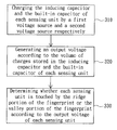
- the method begins at step 310 , the inducing capacitor Cf formed between each sensing unit of the fingerprint acquisition apparatus and the corresponding fingerprint is charged by a first voltage source, and the built-in capacitor Cb is charged by a second voltage source.
- the voltage value of the first voltage source is V 1
- the voltage value of the second voltage source is V 2 .
- an output voltage voltage value is outputted according to the volume of charges stored in the built-in capacitor Cb and the inducing capacitor Cf.
- the output voltage is expressed as (Cf ⁇ V 1 +Cb ⁇ V 2 )/(Cf+Cb).
- each of the sensing units is touched by the ridge portion of the fingerprint or the valley portion of the fingerprint is determined according to the output voltage so as to generate the fingerprint pattern accordingly.
- a threshold can be predetermined according to experiments whereby whether the sensing unit is touched by the ridge portion of the fingerprint or the valley portion of the fingerprint is determined. For example, if the output voltage of a particular sensing unit is larger than the threshold, then the sensing unit is determined to be touched the ridge portion of the fingerprint. If the output voltage of the particular sensing unit is smaller than the threshold, then the sensing unit is determined to be touched the valley portion of the fingerprint.
- the threshold can be determined according to the range of the output voltage of each of the sensing units corresponding to the ridge portion of the fingerprint and the valley portion of the fingerprint.
- the fingerprint acquisition apparatus of the above embodiment of the invention determines whether each of the sensing units is touched by the ridge portion of the fingerprint or the valley portion of the fingerprint by detecting the difference of inducing capacitances between the ridge portion of the fingerprint and the valley portion of the fingerprint, and then generates the fingerprint pattern.
- the invention uses simple circuit structure so that the system complexity is reduced and the apparatus can be directly applied to a single chip and the cost is saved.
Landscapes
- Engineering & Computer Science (AREA)
- Human Computer Interaction (AREA)
- Physics & Mathematics (AREA)
- General Physics & Mathematics (AREA)
- Multimedia (AREA)
- Theoretical Computer Science (AREA)
- Measurement Of Length, Angles, Or The Like Using Electric Or Magnetic Means (AREA)
- Image Input (AREA)
- Measurement Of The Respiration, Hearing Ability, Form, And Blood Characteristics Of Living Organisms (AREA)
Abstract
Description
Claims (12)
Priority Applications (1)
| Application Number | Priority Date | Filing Date | Title |
|---|---|---|---|
| US11/498,959 US7715601B2 (en) | 2005-08-05 | 2006-08-04 | Fingerprint acquisition apparatus and method therefor |
Applications Claiming Priority (2)
| Application Number | Priority Date | Filing Date | Title |
|---|---|---|---|
| US70554905P | 2005-08-05 | 2005-08-05 | |
| US11/498,959 US7715601B2 (en) | 2005-08-05 | 2006-08-04 | Fingerprint acquisition apparatus and method therefor |
Publications (2)
| Publication Number | Publication Date |
|---|---|
| US20070031012A1 US20070031012A1 (en) | 2007-02-08 |
| US7715601B2 true US7715601B2 (en) | 2010-05-11 |
Family
ID=37778571
Family Applications (1)
| Application Number | Title | Priority Date | Filing Date |
|---|---|---|---|
| US11/498,959 Active 2029-03-11 US7715601B2 (en) | 2005-08-05 | 2006-08-04 | Fingerprint acquisition apparatus and method therefor |
Country Status (3)
| Country | Link |
|---|---|
| US (1) | US7715601B2 (en) |
| CN (1) | CN100423019C (en) |
| TW (1) | TWI315852B (en) |
Cited By (1)
| Publication number | Priority date | Publication date | Assignee | Title |
|---|---|---|---|---|
| US20060067564A1 (en) * | 2004-09-30 | 2006-03-30 | Seiko Epson Corporation | Identity authentication device and fingerprint sensor |
Families Citing this family (19)
| Publication number | Priority date | Publication date | Assignee | Title |
|---|---|---|---|---|
| US7663380B2 (en) * | 2007-12-06 | 2010-02-16 | Himax Technologies Limited | Capacitive fingerprint sensor and the panel thereof |
| CN101526989B (en) * | 2008-03-06 | 2011-02-09 | 奇景光电股份有限公司 | Capacitive fingerprint sensor and panel thereof |
| CN101526988B (en) * | 2008-03-06 | 2011-05-04 | 奇景光电股份有限公司 | Capacitive fingerprint sensor and panel thereof |
| US9274553B2 (en) | 2009-10-30 | 2016-03-01 | Synaptics Incorporated | Fingerprint sensor and integratable electronic display |
| US9336428B2 (en) | 2009-10-30 | 2016-05-10 | Synaptics Incorporated | Integrated fingerprint sensor and display |
| US9400911B2 (en) | 2009-10-30 | 2016-07-26 | Synaptics Incorporated | Fingerprint sensor and integratable electronic display |
| CN102289313B (en) * | 2010-06-15 | 2013-10-02 | 周正三 | Composite image sensing apparatus, composite image sensing method and electronic apparatus |
| TWI490789B (en) * | 2011-05-03 | 2015-07-01 | Synaptics Inc | Fingerprint sensor and integratable electronic display |
| CN104898314B (en) | 2014-03-07 | 2018-01-05 | 敦泰电子有限公司 | Display device and its drive circuit and driving method, electronic equipment |
| TWI526945B (en) * | 2014-08-26 | 2016-03-21 | 神盾股份有限公司 | Capacitive fingerprint sensor and fingerprint sensing method thereof |
| TWI526944B (en) * | 2014-10-24 | 2016-03-21 | 義隆電子股份有限公司 | Fingerprint Sensing Device and Method of Detecting Finger Touch Thereof |
| TWI526946B (en) * | 2014-12-17 | 2016-03-21 | 義隆電子股份有限公司 | Fingerprint Detecting Device |
| CN105740756A (en) * | 2014-12-26 | 2016-07-06 | 义隆电子股份有限公司 | Fingerprint Sensing Device And Fingerprint Sensing Method Thereof |
| TWI598827B (en) * | 2015-04-24 | 2017-09-11 | 速博思股份有限公司 | Biometric feature identification device and method |
| TWM516193U (en) * | 2015-06-29 | 2016-01-21 | Round P Technology Co Ltd | Fingerprint recognition sensor with reduced parasitic capacitance |
| US10004432B2 (en) * | 2015-09-01 | 2018-06-26 | Qualcomm Incorporated | Pixel receiver with capacitance cancellation for ultrasonic imaging apparatus |
| CN107664656B (en) * | 2016-07-28 | 2020-06-30 | 奇景光电股份有限公司 | Material identification system and material identification method |
| CN107192937B (en) * | 2017-04-19 | 2019-08-30 | 深圳市中兴移动软件有限公司 | Fingerprint chip detecting method and device, electronic equipment and storage medium |
| US10466576B2 (en) * | 2017-10-20 | 2019-11-05 | Himax Technologies Limited | Method for controlling projector and associated electronic device |
Citations (11)
| Publication number | Priority date | Publication date | Assignee | Title |
|---|---|---|---|---|
| US4353056A (en) * | 1980-06-05 | 1982-10-05 | Siemens Corporation | Capacitive fingerprint sensor |
| TW541503B (en) | 2001-05-17 | 2003-07-11 | Bruce C S Chou | Capacitive pressure microsensor and methods for manufacturing the same and methods for signal detecting the same |
| US6636053B1 (en) * | 2001-11-02 | 2003-10-21 | Stmicroelectronics, Inc. | Capacitive pixel for fingerprint sensor |
| CN1450489A (en) | 2002-04-10 | 2003-10-22 | 祥群科技股份有限公司 | Capacitance type fingerprint access chip |
| US6681033B1 (en) * | 1998-11-16 | 2004-01-20 | Sony Corporation | Capacitance detecting apparatus and its inspecting method and fingerprint checking apparatus |
| TW200424498A (en) | 2003-04-17 | 2004-11-16 | Seiko Epson Corp | Capacitance detection device and drive method thereof, fingerprint sensor, and biometrics authentication device |
| US20040252869A1 (en) * | 2003-06-13 | 2004-12-16 | Satoru Kondo | Image verification system and image verification method |
| US20050018884A1 (en) * | 2003-07-22 | 2005-01-27 | Lg Electronics Inc. | Fingerprint sensor, fabrication method thereof and fingerprint sensing system |
| US20050069178A1 (en) * | 2001-12-07 | 2005-03-31 | Jon Nysaether | Sensor for measurement for wet and dry fingers |
| US20050179446A1 (en) * | 2004-02-17 | 2005-08-18 | Seiko Epson Corporation | Capacitance detection device, fingerprint sensor, biometric authentication device, and method for searching capacitance detection condition |
| US20050253598A1 (en) * | 2004-05-12 | 2005-11-17 | Alps Electric Co., Ltd. | Capacitance detection-type sensor |
Family Cites Families (1)
| Publication number | Priority date | Publication date | Assignee | Title |
|---|---|---|---|---|
| CN1155807C (en) * | 2001-05-25 | 2004-06-30 | 周正三 | Capacitance-type micro pressure-sensing element and its making process and signal reading method |
-
2006
- 2006-08-04 CN CNB2006101101700A patent/CN100423019C/en active Active
- 2006-08-04 US US11/498,959 patent/US7715601B2/en active Active
- 2006-08-04 TW TW095128733A patent/TWI315852B/en active
Patent Citations (11)
| Publication number | Priority date | Publication date | Assignee | Title |
|---|---|---|---|---|
| US4353056A (en) * | 1980-06-05 | 1982-10-05 | Siemens Corporation | Capacitive fingerprint sensor |
| US6681033B1 (en) * | 1998-11-16 | 2004-01-20 | Sony Corporation | Capacitance detecting apparatus and its inspecting method and fingerprint checking apparatus |
| TW541503B (en) | 2001-05-17 | 2003-07-11 | Bruce C S Chou | Capacitive pressure microsensor and methods for manufacturing the same and methods for signal detecting the same |
| US6636053B1 (en) * | 2001-11-02 | 2003-10-21 | Stmicroelectronics, Inc. | Capacitive pixel for fingerprint sensor |
| US20050069178A1 (en) * | 2001-12-07 | 2005-03-31 | Jon Nysaether | Sensor for measurement for wet and dry fingers |
| CN1450489A (en) | 2002-04-10 | 2003-10-22 | 祥群科技股份有限公司 | Capacitance type fingerprint access chip |
| TW200424498A (en) | 2003-04-17 | 2004-11-16 | Seiko Epson Corp | Capacitance detection device and drive method thereof, fingerprint sensor, and biometrics authentication device |
| US20040252869A1 (en) * | 2003-06-13 | 2004-12-16 | Satoru Kondo | Image verification system and image verification method |
| US20050018884A1 (en) * | 2003-07-22 | 2005-01-27 | Lg Electronics Inc. | Fingerprint sensor, fabrication method thereof and fingerprint sensing system |
| US20050179446A1 (en) * | 2004-02-17 | 2005-08-18 | Seiko Epson Corporation | Capacitance detection device, fingerprint sensor, biometric authentication device, and method for searching capacitance detection condition |
| US20050253598A1 (en) * | 2004-05-12 | 2005-11-17 | Alps Electric Co., Ltd. | Capacitance detection-type sensor |
Cited By (2)
| Publication number | Priority date | Publication date | Assignee | Title |
|---|---|---|---|---|
| US20060067564A1 (en) * | 2004-09-30 | 2006-03-30 | Seiko Epson Corporation | Identity authentication device and fingerprint sensor |
| US7835553B2 (en) * | 2004-09-30 | 2010-11-16 | Seiko Epson Corporation | Identity authentication device and fingerprint sensor |
Also Published As
| Publication number | Publication date |
|---|---|
| CN100423019C (en) | 2008-10-01 |
| TWI315852B (en) | 2009-10-11 |
| TW200723131A (en) | 2007-06-16 |
| CN1920851A (en) | 2007-02-28 |
| US20070031012A1 (en) | 2007-02-08 |
Similar Documents
| Publication | Publication Date | Title |
|---|---|---|
| US7715601B2 (en) | Fingerprint acquisition apparatus and method therefor | |
| US8415957B2 (en) | Capacitance measurement circuit and method | |
| US20110163994A1 (en) | Touch sensing system, capacitance sensing apparatus and capacitance sensing method thereof | |
| US10990230B2 (en) | Circuit, touch chip, and electronic device for capacitance detection | |
| US20100098303A1 (en) | Fingerprint detection device and method and associated touch control device with fingerprint detection | |
| US20140092061A1 (en) | Semiconductor device and electronic device | |
| US20180005004A1 (en) | Touch detection circuit, fingerprint module and control method thereof | |
| JP5826971B2 (en) | Stylus pen, touch panel system, and electronic device | |
| KR20180061539A (en) | Touch Display Device, Display Panel, Touch Sensing Method, Touch Sensing Circuit, and Driving Circuit | |
| Park et al. | A pen-pressure-sensitive capacitive touch system using electrically coupled resonance pen | |
| CN110008860B (en) | Fingerprint identification framework and touch panel | |
| CN216053107U (en) | Capacitive fingerprint sensing device | |
| US11009993B2 (en) | Fingerprint recognition touch sensor and electronic apparatus including the same | |
| US11853098B2 (en) | Detection circuit, touch control panel, and electronic apparatus | |
| US10921158B2 (en) | Power supply generating circuit, capacitive array sensing apparatus and terminal device | |
| CN110796983A (en) | Display device and driving method thereof | |
| JP2009223884A (en) | Control method, circuit, and electronic system utilizing the same | |
| US8400420B2 (en) | Image display system and method for controlling a touch panel thereof | |
| US11093090B2 (en) | TFT-based fingerprint sensing system with corrected read-out | |
| US10969912B2 (en) | Capacitive sensing and sampling circuit and sensing and sampling method thereof | |
| CN111404536A (en) | Capacitance detection circuit of touch device, touch device and electronic equipment | |
| US20190294272A1 (en) | Touch controller and touchscreen device | |
| EP3493096A1 (en) | Fingerprint sensor and terminal device | |
| US20240062574A1 (en) | Fingerprint sensing system with current control | |
| KR101765443B1 (en) | Touch sensing system having improved sensing performance |
Legal Events
| Date | Code | Title | Description |
|---|---|---|---|
| AS | Assignment |
Owner name: HIMAX TECHNOLOGIES, INC.,TAIWAN Free format text: ASSIGNMENT OF ASSIGNORS INTEREST;ASSIGNORS:SHEU, MENG-LIEH;YANG, HUNG-MING;REEL/FRAME:018447/0386 Effective date: 20061012 Owner name: NATIONAL CHI NAN UNIVERSITY,TAIWAN Free format text: ASSIGNMENT OF ASSIGNORS INTEREST;ASSIGNORS:SHEU, MENG-LIEH;YANG, HUNG-MING;REEL/FRAME:018447/0386 Effective date: 20061012 Owner name: NATIONAL CHI NAN UNIVERSITY, TAIWAN Free format text: ASSIGNMENT OF ASSIGNORS INTEREST;ASSIGNORS:SHEU, MENG-LIEH;YANG, HUNG-MING;REEL/FRAME:018447/0386 Effective date: 20061012 Owner name: HIMAX TECHNOLOGIES, INC., TAIWAN Free format text: ASSIGNMENT OF ASSIGNORS INTEREST;ASSIGNORS:SHEU, MENG-LIEH;YANG, HUNG-MING;REEL/FRAME:018447/0386 Effective date: 20061012 |
|
| AS | Assignment |
Owner name: HIMAX TECHNOLOGIES LIMITED, TAIWAN Free format text: CORRECTIVE COVER SHEET TO CORRECT THE NAME OF THE ASSIGNEE THAT WAS PREVIOUSLY RECORDED ON REEL 018447 FRAME 0386.;ASSIGNORS:SHEU, MENG-LIEH;YANG, HUNG-MING;REEL/FRAME:020789/0441 Effective date: 20061012 Owner name: NATIONAL CHI NAN UNIVERSITY, TAIWAN Free format text: CORRECTIVE COVER SHEET TO CORRECT THE NAME OF THE ASSIGNEE THAT WAS PREVIOUSLY RECORDED ON REEL 018447 FRAME 0386.;ASSIGNORS:SHEU, MENG-LIEH;YANG, HUNG-MING;REEL/FRAME:020789/0441 Effective date: 20061012 Owner name: HIMAX TECHNOLOGIES LIMITED,TAIWAN Free format text: CORRECTIVE COVER SHEET TO CORRECT THE NAME OF THE ASSIGNEE THAT WAS PREVIOUSLY RECORDED ON REEL 018447 FRAME 0386;ASSIGNORS:SHEU, MENG-LIEH;YANG, HUNG-MING;REEL/FRAME:020789/0441 Effective date: 20061012 Owner name: NATIONAL CHI NAN UNIVERSITY,TAIWAN Free format text: CORRECTIVE COVER SHEET TO CORRECT THE NAME OF THE ASSIGNEE THAT WAS PREVIOUSLY RECORDED ON REEL 018447 FRAME 0386;ASSIGNORS:SHEU, MENG-LIEH;YANG, HUNG-MING;REEL/FRAME:020789/0441 Effective date: 20061012 |
|
| STCF | Information on status: patent grant |
Free format text: PATENTED CASE |
|
| FPAY | Fee payment |
Year of fee payment: 4 |
|
| MAFP | Maintenance fee payment |
Free format text: PAYMENT OF MAINTENANCE FEE, 8TH YEAR, LARGE ENTITY (ORIGINAL EVENT CODE: M1552) Year of fee payment: 8 |
|
| AS | Assignment |
Owner name: CAPACITANT INNOVATIONS LLC, DELAWARE Free format text: ASSIGNMENT OF ASSIGNORS INTEREST;ASSIGNOR:HIMAX TECHNOLOGIES LIMITED;REEL/FRAME:052461/0407 Effective date: 20200317 |
|
| AS | Assignment |
Owner name: HIMAX TECHNOLOGIES LIMITED, TAIWAN Free format text: ASSIGNMENT OF ASSIGNORS INTEREST;ASSIGNOR:CAPACITANT INNOVATIONS LLC;REEL/FRAME:054160/0117 Effective date: 20200918 |
|
| MAFP | Maintenance fee payment |
Free format text: PAYMENT OF MAINTENANCE FEE, 12TH YEAR, LARGE ENTITY (ORIGINAL EVENT CODE: M1553); ENTITY STATUS OF PATENT OWNER: LARGE ENTITY Year of fee payment: 12 |