US7700962B2 - Inverted-pyramidal photonic crystal light emitting device - Google Patents
Inverted-pyramidal photonic crystal light emitting device Download PDFInfo
- Publication number
- US7700962B2 US7700962B2 US11/564,213 US56421306A US7700962B2 US 7700962 B2 US7700962 B2 US 7700962B2 US 56421306 A US56421306 A US 56421306A US 7700962 B2 US7700962 B2 US 7700962B2
- Authority
- US
- United States
- Prior art keywords
- light
- layer
- led
- semiconductor material
- inverted
- Prior art date
- Legal status (The legal status is an assumption and is not a legal conclusion. Google has not performed a legal analysis and makes no representation as to the accuracy of the status listed.)
- Active, expires
Links
- 239000004038 photonic crystal Substances 0.000 title description 52
- 239000000463 material Substances 0.000 claims abstract description 82
- 238000000034 method Methods 0.000 claims abstract description 52
- 238000000605 extraction Methods 0.000 claims abstract description 48
- 239000004065 semiconductor Substances 0.000 claims abstract description 40
- 238000007373 indentation Methods 0.000 claims abstract description 33
- 230000000694 effects Effects 0.000 claims abstract description 14
- 229920002120 photoresistant polymer Polymers 0.000 claims description 24
- 230000008569 process Effects 0.000 claims description 22
- 230000003287 optical effect Effects 0.000 claims description 14
- 238000000926 separation method Methods 0.000 claims description 11
- 238000009826 distribution Methods 0.000 claims description 10
- 239000013079 quasicrystal Substances 0.000 claims description 10
- 239000000758 substrate Substances 0.000 claims description 10
- 239000013078 crystal Substances 0.000 claims description 9
- 238000000059 patterning Methods 0.000 claims description 8
- 238000000151 deposition Methods 0.000 claims description 7
- 238000001039 wet etching Methods 0.000 claims description 5
- 230000001902 propagating effect Effects 0.000 claims description 4
- 230000007547 defect Effects 0.000 claims description 3
- 238000000347 anisotropic wet etching Methods 0.000 abstract 1
- 229910002601 GaN Inorganic materials 0.000 description 36
- JMASRVWKEDWRBT-UHFFFAOYSA-N Gallium nitride Chemical compound [Ga]#N JMASRVWKEDWRBT-UHFFFAOYSA-N 0.000 description 23
- 238000004519 manufacturing process Methods 0.000 description 17
- 235000012431 wafers Nutrition 0.000 description 9
- 238000013461 design Methods 0.000 description 8
- 238000005530 etching Methods 0.000 description 7
- HEMHJVSKTPXQMS-UHFFFAOYSA-M Sodium hydroxide Chemical compound [OH-].[Na+] HEMHJVSKTPXQMS-UHFFFAOYSA-M 0.000 description 6
- 230000008878 coupling Effects 0.000 description 5
- 238000010168 coupling process Methods 0.000 description 5
- 238000005859 coupling reaction Methods 0.000 description 5
- 229910052751 metal Inorganic materials 0.000 description 5
- 239000002184 metal Substances 0.000 description 5
- 238000005498 polishing Methods 0.000 description 5
- VYPSYNLAJGMNEJ-UHFFFAOYSA-N Silicium dioxide Chemical compound O=[Si]=O VYPSYNLAJGMNEJ-UHFFFAOYSA-N 0.000 description 4
- 230000002411 adverse Effects 0.000 description 4
- 230000015572 biosynthetic process Effects 0.000 description 4
- 238000001459 lithography Methods 0.000 description 4
- 238000004088 simulation Methods 0.000 description 4
- 238000004544 sputter deposition Methods 0.000 description 4
- 229910002704 AlGaN Inorganic materials 0.000 description 3
- KWYUFKZDYYNOTN-UHFFFAOYSA-M Potassium hydroxide Chemical compound [OH-].[K+] KWYUFKZDYYNOTN-UHFFFAOYSA-M 0.000 description 3
- 239000006185 dispersion Substances 0.000 description 3
- 230000008020 evaporation Effects 0.000 description 3
- 238000001704 evaporation Methods 0.000 description 3
- 238000000623 plasma-assisted chemical vapour deposition Methods 0.000 description 3
- 238000012545 processing Methods 0.000 description 3
- HBMJWWWQQXIZIP-UHFFFAOYSA-N silicon carbide Chemical compound [Si+]#[C-] HBMJWWWQQXIZIP-UHFFFAOYSA-N 0.000 description 3
- 229910010271 silicon carbide Inorganic materials 0.000 description 3
- 230000003746 surface roughness Effects 0.000 description 3
- 241001270131 Agaricus moelleri Species 0.000 description 2
- NBIIXXVUZAFLBC-UHFFFAOYSA-N Phosphoric acid Chemical compound OP(O)(O)=O NBIIXXVUZAFLBC-UHFFFAOYSA-N 0.000 description 2
- 229910052581 Si3N4 Inorganic materials 0.000 description 2
- 229910052681 coesite Inorganic materials 0.000 description 2
- 229910052906 cristobalite Inorganic materials 0.000 description 2
- 230000007613 environmental effect Effects 0.000 description 2
- 238000001093 holography Methods 0.000 description 2
- 230000006872 improvement Effects 0.000 description 2
- 229910001092 metal group alloy Inorganic materials 0.000 description 2
- 230000010363 phase shift Effects 0.000 description 2
- 238000007517 polishing process Methods 0.000 description 2
- 229910052594 sapphire Inorganic materials 0.000 description 2
- 239000010980 sapphire Substances 0.000 description 2
- 238000001878 scanning electron micrograph Methods 0.000 description 2
- 239000000377 silicon dioxide Substances 0.000 description 2
- 229910052709 silver Inorganic materials 0.000 description 2
- 239000004332 silver Substances 0.000 description 2
- 239000007787 solid Substances 0.000 description 2
- 239000000243 solution Substances 0.000 description 2
- 230000007480 spreading Effects 0.000 description 2
- 238000003892 spreading Methods 0.000 description 2
- 229910052682 stishovite Inorganic materials 0.000 description 2
- 238000012546 transfer Methods 0.000 description 2
- 238000013519 translation Methods 0.000 description 2
- 229910052905 tridymite Inorganic materials 0.000 description 2
- 229910000530 Gallium indium arsenide Inorganic materials 0.000 description 1
- 238000013459 approach Methods 0.000 description 1
- 230000004888 barrier function Effects 0.000 description 1
- 230000009286 beneficial effect Effects 0.000 description 1
- 238000005229 chemical vapour deposition Methods 0.000 description 1
- 230000002301 combined effect Effects 0.000 description 1
- 239000002131 composite material Substances 0.000 description 1
- 239000004020 conductor Substances 0.000 description 1
- 230000008021 deposition Effects 0.000 description 1
- 238000001312 dry etching Methods 0.000 description 1
- 238000005516 engineering process Methods 0.000 description 1
- 230000005496 eutectics Effects 0.000 description 1
- 230000004907 flux Effects 0.000 description 1
- PCHJSUWPFVWCPO-UHFFFAOYSA-N gold Chemical compound [Au] PCHJSUWPFVWCPO-UHFFFAOYSA-N 0.000 description 1
- 229910052737 gold Inorganic materials 0.000 description 1
- 239000010931 gold Substances 0.000 description 1
- 238000002347 injection Methods 0.000 description 1
- 239000007924 injection Substances 0.000 description 1
- 239000004973 liquid crystal related substance Substances 0.000 description 1
- 230000000873 masking effect Effects 0.000 description 1
- 239000007769 metal material Substances 0.000 description 1
- 229910003465 moissanite Inorganic materials 0.000 description 1
- 230000000737 periodic effect Effects 0.000 description 1
- 238000000206 photolithography Methods 0.000 description 1
- 230000005855 radiation Effects 0.000 description 1
- 230000006798 recombination Effects 0.000 description 1
- 238000005215 recombination Methods 0.000 description 1
- 238000004064 recycling Methods 0.000 description 1
- 238000002310 reflectometry Methods 0.000 description 1
- 229910052710 silicon Inorganic materials 0.000 description 1
- 239000010703 silicon Substances 0.000 description 1
- 239000000126 substance Substances 0.000 description 1
Images


Classifications
-
- H—ELECTRICITY
- H01—ELECTRIC ELEMENTS
- H01L—SEMICONDUCTOR DEVICES NOT COVERED BY CLASS H10
- H01L33/00—Semiconductor devices having potential barriers specially adapted for light emission; Processes or apparatus specially adapted for the manufacture or treatment thereof or of parts thereof; Details thereof
- H01L33/02—Semiconductor devices having potential barriers specially adapted for light emission; Processes or apparatus specially adapted for the manufacture or treatment thereof or of parts thereof; Details thereof characterised by the semiconductor bodies
- H01L33/20—Semiconductor devices having potential barriers specially adapted for light emission; Processes or apparatus specially adapted for the manufacture or treatment thereof or of parts thereof; Details thereof characterised by the semiconductor bodies with a particular shape, e.g. curved or truncated substrate
-
- H—ELECTRICITY
- H01—ELECTRIC ELEMENTS
- H01L—SEMICONDUCTOR DEVICES NOT COVERED BY CLASS H10
- H01L2933/00—Details relating to devices covered by the group H01L33/00 but not provided for in its subgroups
- H01L2933/0083—Periodic patterns for optical field-shaping in or on the semiconductor body or semiconductor body package, e.g. photonic bandgap structures
Definitions
- the present invention relates to light-emitting diodes with improved light extraction and directionality, and in particular to devices employing photonic crystal structures.
- LEDs Light emitting diodes
- LEDs are based on a forward biased p-n junction and have recently reached sufficiently high brightness levels that they are now suitable for new solid-state lighting applications as well as replacements for projector light sources. Entry into these markets has also been enabled by the economical gains achieved through the high efficiencies of LEDs, as well as reliability, long lifetime and environmental benefits. In particular, applications in solid-state lighting require that LEDs exceed efficiencies currently achievable by alternative fluorescent lighting technologies.
- Back Light Units (BLU) for liquid crystal display (LCD) panels are key elements in the performance of an LCD panel.
- LCD panels employ compact cathode fluorescent light (ccfl) sources.
- ccfl compact cathode fluorescent light
- these sources suffer from several problems, including poor colour gamut, environmental recycling and manufacture issues, thickness and profile, high voltage requirements, poor thermal management, weight and high power consumption.
- LED BLU units offer benefits in many areas, including colour gamut, lower power consumption, thin profiles, low voltage requirements, good thermal management and low weight.
- a more isotropic or Lambertian light distribution from an LED is desired and one technique used to achieve this is to roughen the surface through which the light merges.
- a certain degree of roughness is inherent depending on the LED fabrication process.
- etching a controlled degree of increased surface roughness can be achieved to improve the scrambling and uniformity of light emerging from the LED.
- US2006/0181899 and US2006/0181903 disclose an optical light guide or waveguide arranged to evenly distribute diffused light across the complete LCD panel surface.
- the light is coupled into the light guide by using side-mounted LED optical sources.
- Side mounting is beneficial as the number of LEDs required is dramatically reduced per unit area of backlit LCD, when compared with direct LED backlighting. It is proposed that a 32 inch LCD panel can be side lit with as few as 12 LED sources. However, to maximise the light diffused onto the LCD panel the most optimal coupling of the LED light into the light guide is required.
- High Intensity Discharge (HID) type projector light engines have always been hindered by low efficiency and short lifetime, resulting in slow adoption into consumer markets.
- the Etendue value of the light source needs to be smaller or matched to the microdisplay Etendue value. This compatibility is very important for improving the overall system efficiency of the complete light projection engine.
- high total luminous outputs and low power consumption are also very important, especially in applications where large rear projection screens (bigger than 50 inch) and front projection systems are required. Low power consumption is desirable in order to minimise thermal management issues.
- the overall efficiency of an LED can be quantified by three main factors, namely internal quantum efficiency, injection efficiency, and extraction efficiency.
- One of the main limiting factors reducing the efficiency of light extraction from an LED is total internal reflection of the emitted photons and their trapping in the high refractive index of the epi-material forming the LED. These trapped waveguide modes propagate in the LED structure until they are scattered or reabsorbed. The thickness of the LED structure determines the number of modes that can be supported.
- U.S. Pat. No. 5,779,924 and U.S. Pat. No. 5,955,749 both describe the use of photonic crystal patterns defined in the semiconductor layers of the LED to affect the way light propagates through the epi-structure.
- the photonic band structure formed allows the trapped modes to be extracted out and hence increase the extraction efficiency and ultimately the total external efficiency of the LED.
- the use of photonic crystal structures in an LED is advantageous over other light extraction techniques as they scale with the active surface area of the LED and hence provide an ideal means for improving the light extraction for a large-area high-brightness LED die.
- the scaling of the LED size is important for solid state lighting applications where absolute luminous output is required
- the total light extraction for many of these photonic crystal LEDs is not as high as for more conventional surface-roughened LEDs.
- U.S. Pat. No. 6,831,302 and US2005/0285132 describe processes for fabricating light-emitting diodes with photonic crystal structures using Gallium Nitride (GaN) based materials. In both cases the processing involves many complex and expensive steps that ultimately affect the yield and cost of the LED wafers. In particular, U.S. Pat. No.
- 6,831,302 describes a fabrication process that involves the following steps: growing an n-GaN layer on a lattice matched single crystal wafer, an active QW region, and a p-GaN layer, followed by eutectic bonding of a sub-mount or substrate on the top surface, wafer flipping, lift-off from the growth wafer (using a technique such as laser lift-off), surface polishing to provide an optically-smooth surface (using a process such as chemical mechanical polishing), definition of a photonic crystal pattern on the surface (by a process such as nano-imprinting, lithography, or holography), and finally photonic crystal pattern transfer into the GaN material using a suitable dry (egg. RIE or ICP) or wet etch of the GaN.
- a suitable dry egg. RIE or ICP
- One of the complex processing steps involved is the polishing of the wafers, which can adversely affect the yield due to the difficulty in controlling the surface quality across the complete wafer. Small scratches across the surface may affect the current spreading across the LED wafer and ultimately provide a path to short circuiting the complete LED or adversely affecting the forward voltage.
- the thickness of the GaN epi-structure is important for the effective design of the photonic crystal extraction pattern
- the high refractive index acts like a highly-multimode waveguide, whereby the thickness determines the number of modes residing in the LED heterostructure.
- Another complex fabrication step is the definition of small-scale first-order photonic crystal features in the range of 300 nm to 500 nm for the pitch of the features and in the range of 200 nm to 400 nm for the diameter of the hole features.
- Such patterns are currently defined using either nano-imprinting or holography.
- the former technique is currently not a proven technique for such small-scale features on LED wafers and only low yields are achieved.
- the technique suffers from a higher cost for small manufacturing volumes.
- the latter lithography technique suffers from complex alignment and stability as well as low volumes.
- a light-emitting device comprises:
- a first layer comprising a first semiconductor material having a first type of doping
- a second layer comprising a second semiconductor material having a second type of doping
- a light-generating layer disposed between the first and second layers
- the first layer has an upper surface distal the light-generating layer and a lower surface proximate the light-generating layer and wherein light generated in the light-generating layer emerges from the LED structure through the upper surface of the first layer, the first layer further comprising a tiling arrangement of inverted pyramidal or inverted frustro-pyramidal indentations in the first semiconductor material extending from the upper surface towards the light-generating layer and comprising a material of different refractive index to the first semiconductor material, wherein the tiling arrangement of indentations and surrounding first semiconductor material comprise a photonic band structure, and wherein the indentations and their tiling arrangement are configured such that light emerging from the LED structure through the upper surface is substantially more directional than from a Lambertian source.
- a Lambertian source emits a luminous flux per unit solid angle that in any direction is proportional to the cosine of the angle between that direction and the normal to the surface from which it is emitted. This leads to a uniform radiance with a spherical distribution.
- An LED comprising a structure according to the present invention combines greater directionality of emitted light with an improvement in the efficiency with which light generated by the device is coupled into the emitted beam. This is achieved through the innovative tiling arrangement of pyramidal, or frustro-pyramidal, surface indentations.
- photonic tiling arrangements Three particular classes of photonic tiling arrangements are preferred, namely photonic crystals having both short range and long range order, photonic quasicrystals having short range translation disorder but long range order, amorphous tiling patterns having short range separation order but long range disorder.
- photonic crystals having both short range and long range order
- photonic quasicrystals having short range translation disorder but long range order
- amorphous tiling patterns having short range separation order but long range disorder.
- the separation between neighbouring inverted pyramidal regions is fixed while the rotational symmetry is randomised.
- a high-order inverted pyramidal photonic crystal or quasicrystal pattern is proposed that provides increased light extraction when compared to more conventional first-order photonic crystal patterns.
- Careful design of the photonic crystal also allows tailoring of the far-field light pattern produced by the device.
- the inverted pyramidal shape of the indentations with angled side walls and their well-defined tiling arrangement can extract light from the LED in a beam that is more collimated than a from Lambertian source, even for patterns with large lattice constants (>1 ⁇ m).
- the inverted pyramidal indentations have a size greater than 1.0 ⁇ m. However, they may be greater than 1.5 ⁇ m or 2.0 ⁇ m in size or even greater than 2.5 ⁇ m in size.
- the relatively large inverted pyramid sizes relaxes the tolerances for fabrication and also means that surface polishing is not required prior to formation of the inverted pyramidal indentations, as their dimensions are sufficiently greater than the residual surface roughness.
- the pitch of the tiling arrangement is greater than 1.5 ⁇ m, although it may be greater than 2.0 ⁇ m or 2.5 ⁇ m in size or even greater than 3.0 ⁇ m in size.
- the indentations are configured such that a significant proportion (>35%) of the light is extracted in a central cone having a 30° half-angle to the vertical axis. Preferably, greater than 37%, 38% or even 40% is extracted in the central cone. This enables efficient and uniform coupling of light into narrow elongated light guides that are often used with light sources for projection applications.
- the inverted pyramids and tiling pattern may be configured such that light is predominantly extracted at angles greater than this, in a side-emitting fashion.
- light may be emitted in a collimated ring or donut-like distribution around the vertical axis, rather than within a narrow central cone.
- the distribution may be centred at angles greater than or equal to 30°, 40°, 50° or 60° to the vertical, or equivalently at angles less than or equal to 60°, 50°, 40° or 30° to the surface.
- the first semiconductor material having the first type of doping may be either n-doped or p-doped, in which case the second semiconductor material having the second type of doping will be either p-doped or n-doped, respectively.
- the first layer may comprise a layer of etch stop material embedded at a predetermined depth in the first semiconductor material, in which case the inverted pyramidal indentations will extend down to the etch stop material layer.
- the first semiconductor material comprises n-doped GaN or InGaN and the second semiconductor material comprises p-doped GaN or InGaN.
- the light-generating layer comprises a multiple quantum well structure of GaN—InGaN.
- the higher order photonic crystal dimensions are typically in the range 1.0 ⁇ m to 3.0 ⁇ m, although this depends on a range of factors, including wavelength, far-field pattern, LED thickness and location of the multiple quantum well structure within the overall GaN heterostructure.
- Suitable etch stop materials include AlGaN and InGaN.
- the LED further comprises an optical reflector to reflect light propagating away from the upper extraction surface of the first layer and which would otherwise not be extracted.
- the optical reflector is disposed adjacent the second layer of the second semiconductor material such that the second layer is located between the light-generating layer and the reflector.
- the optical reflector comprises a simple layer of a metallic material or it may comprise a multi-layer dielectric structure.
- the optical reflector may comprise a distributed Bragg reflector (DBR) or an omni-directional reflector (ODR).
- DBR distributed Bragg reflector
- ODR omni-directional reflector
- a separation distance between the light-generating layer and the optical reflector is such as to comprise a microcavity which enhances the amount of generated light propagating towards the upper extraction surface of the first layer.
- the microcavity effect gives an even greater enhancement in extraction efficiency over and above that provided by simple reflection at the optical reflector.
- An optimal separation is between 0.5 to 0.7 times the wavelength of light generated in the light-generating layer.
- the inverted pyramidal indentations and their tiling arrangement are configured to cooperate optimally with the microcavity effect to further enhance the efficiency of light extraction from the LED.
- the LED described above is suitable for application in solid-state lighting sources, including those for front and rear projectors.
- a light engine for an optical projector unit comprises a plurality of light emitting devices according to the first aspect.
- a method for fabricating a light-emitting device (LED) according to the first aspect comprises the steps of:
- a light-emitting device heterostructure comprising a first layer comprising a first semiconductor material having a first type of doping, a second layer comprising a second semiconductor material having a second type of doping, and a light-generating layer disposed between the first and second layers, wherein the first layer has an upper surface distal the light-generating layer and a lower surface proximate the light-generating layer and wherein light generated in the light-generating layer emerges from the LED structure through the upper surface of the first layer,
- the step of forming the mask comprises the steps of:
- the indentations comprising a material of different refractive index to the surrounding first semiconductor material and which together comprise a photonic band structure.
- the light-emitting device heterostructure itself may be fabricated by any suitable known process, including flip-chip processes.
- the layer of photoresist may itself be the mask layer, in which case the islands of mask material are the islands of photoresist. Any suitable process for patterning the photoresist by exposure may be used, including UV lithography.
- the un-exposed photoresist is removed using a suitable developer and the remaining exposed photoresist removed by stripping.
- a variety of etchants are available for the anisotropic wet etch, including solutions of KOH, NaOH or H 3 PO 4 .
- a harder mask material may be employed, which is etch-resistant to the anisotropic wet etch.
- the step of forming an etch mask further comprises the steps of:
- Suitable hard mask materials include SiO 2 or Si 3 N 4 deposited by PECVD or a metal deposited by sputtering or evaporation. Once the pyramidal protrusions have been formed, the remaining hard mask material surrounding the islands is removed by a suitable wet or dry etch process.
- the depth of the anisotropic etch will determine the size of the indentations formed.
- precise control of the anisotropic etch depth may be difficult, if based on speed of etch and etch time.
- the etch stop is required in order to form inverted frustro-pyramidal indentations.
- the first layer of the light-emitting device heterostructure comprises a layer of etch stop material embedded at the predetermined depth in the first semiconductor material.
- the anisotropic etch of the first semiconductor material will then continue until the layer of etch stop material is reached, thus providing greater uniformity and repeatability of the fabrication method and also permitting the formation of inverted flat-top or truncated pyramidal indentations.
- the present invention also provides a simplified method of manufacture of a photonic crystal type LED structure, whereby the definition of a large feature photonic crystal is transferred onto an LED by the use of low cost photolithography or similar process and without the need for complex polishing processes.
- FIG. 1 shows a cross section of the proposed device
- FIG. 2A shows inverted pyramids arranged in a regular square lattice
- FIG. 2B shows inverted pyramids arranged in a 12-fold quasicrystal
- FIG. 3 shows normalised light intensity of a GaN LED as a function of quantum well to mirror separation distance
- FIGS. 4A to 4D illustrate a Flip Chip-based manufacturing process for fabricating a light emitting device
- FIGS. 4E to 4I or 4 J illustrate the additional manufacturing steps for fabricating an inverted pyramidal or truncated inverted pyramidal photonic crystal structure in the upper layer of the device shown in FIG. 4D ;
- FIG. 5A shows the enhancement in light extraction in a 30° cone for a pyramidal PC-LED as compared to an un-patterned device
- FIG. 5B shows the enhancement in total light extraction for a pyramidal PC-LED as compared to an un-patterned device
- FIG. 5C shows the percentage of light in the 30° cone for different pyramidal photonic crystal light emitting devices
- FIG. 6 shows the far-field pattern for a PC-LED structure according to a preferred embodiment of the invention
- FIG. 7 shows an SEM micrograph of an isolated inverted pyramid formed using the fabrication method of the invention
- FIG. 8A is a plot of light extraction enhancement versus photonic crystal fill fraction for a conventional PC-LED and for an inverted pyramidal PC-LED with micro-cavity compared to an un-patterned LED;
- FIG. 8B is a plot of light extraction enhancement versus photonic crystal fill fraction for an inverted pyramidal PC-LED compared to an un-patterned LED with and without micro-cavity;
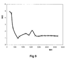
- FIG. 9 is a plot of light extraction enhancement versus LED heterostructure core thickness for an inverted pyramidal PC-LED compared to an un-patterned LED.
- An aim of the present invention is to provide improved light extraction as well as tailored far-field emission from light emitting devices.
- These devices can employ a wide range of light emitting semiconductor material system including, but not restricted to, InGaN, InGaP, InGaAs, InP, or ZnO.
- the description will focus on the implementation of the directional light extraction technique implemented in green InGaN light emitting devices.
- the design can be equally optimised and implemented for other emission wavelengths (such as blue or UV) using this material as well as for other material systems, such as InGaP which is suitable for red and yellow wavelengths.
- a novel high-order inverted pyramidal photonic crystal (PC) or quasicrystal pattern is proposed that provides increased light extraction, as compared to first-order photonic crystal patterns.
- the PC design also allows for the tailoring of the far-field light distribution emitted by the devices.
- the inverted pyramidal shape of the PC sub-regions and their well defined tiling arrangement permits extraction of light from the device in a beam which is more collimated than from a Lambertian source. A simplified process for manufacturing the device will also be described.
- the higher-order PC dimensions are greater than 1.0 ⁇ m in size and may be greater than 1.5 ⁇ m or 2.0 ⁇ m, and can be up to, but not limited to, 3.0 ⁇ m, 3.5 ⁇ m and 4.0 ⁇ m in size. This varies depending on the far-field pattern, the LED thickness and the location of the quantum wells within the light-generating region of the GaN heterostructure.
- FIG. 1 demonstrates a cross section of the proposed light emitting device, which comprises pyramids 101 etched in the n-doped GaN or InGaN layer in a periodic, quasicrystalline, amorphous or other complex ordered or repeating tiling arrangement.
- the pyramidal tiling arrangement is designed to provide dispersion bands that allow trapped light to couple into the Bloch modes of the photonic crystal. Once the light is coupled into the Bloch modes, the photonic crystal provides a means of coupling the light out into free space.
- the device shown in FIG. 1 comprises a light-emitting heterostructure, which includes an n-GaN or InGaN top layer 102 and a lower p-type GaN or InGaN layer 104 with a multiple quantum well (MQW) structure 103 residing between these layers.
- MQW multiple quantum well
- Beneath the p-type layer 104 a reflector layer 105 is present, which can be in the form of a metal reflector such as silver or in the form of a DBR or omni-directional reflector (ODR).
- the light emitting structure is supported by a carrier substrate or mount, 106 .
- the carrier substrate comprises an electrically conductive material with a high thermal conductivity such as metal or metal alloy or alternatively Silicon or Silicon Carbide.
- photonic tiling arrangements which are preferred in the present invention, and in which the arrangements possess the following properties: short range and long range order, namely photonic crystals; short range translation disorder but possess long range order, namely photonic quasicrystals; and short range separation order and long range disorder, namely amorphous tiling arrangements.
- short range and long range order namely photonic crystals
- short range translation disorder but possess long range order namely photonic quasicrystals
- short range separation order and long range disorder namely amorphous tiling arrangements.
- amorphous tiling arrangements the separation between neighbouring inverted pyramidal regions is fixed while the rotational symmetry is randomised.
- These classes of patterning can also comprise of repeating cells of the above-mentioned tiling arrangements. Additionally, they can comprise of regions with defects, that is to say regions where inverted pyramids are removed or the shape or size of the inverted pyramids is modified. The sub-regions may also comprise of inverted pyramids with unetched sharp apex regions, giving rise to flat-top (frustro) inverted pyramids.
- the patterning can be characterised by a number of parameters, including the pitch a of the lattice defined as the distance separating the centres of two neighbouring inverted pyramids, and the angle ⁇ formed between the inverted pyramid crystallographic exposed face and the horizontal crystal plane of the GaN lattice.
- One of the main aspects of the present invention is the use of large features that are crystallographically aligned to provide maximum pattern reproduction accuracy as well as relaxed positional accuracy.
- the hexagonal inverted pyramids (that are formed in c-plane GaN) can be arranged in a regular pattern, quasicrystalline pattern, amorphous pattern or other suitable arrangement.
- An example is shown in FIG. 2A where the hexagonal inverted pyramids are arranged in a regular square lattice to form a photonic crystal.
- FIG. 2B shows inverted pyramids arranged in a 12-fold symmetric square-triangle quasicrystal tiling to form a photonic quasicrystal.
- An enhanced version of the invention employs an optical reflector placed somewhere below the light emitting region to reflect downward propagating light in the upward direction Moreover, the separation distance between the light emitting region and the reflector is designed to enhance upward emitting light due to the so-called microcavity effect.
- the inverted pyramidal photonic crystal is then optimised in conjunction with the microcavity effect to further enhance light extraction. As described by Shen in Appl. Phys. Lett.
- w 0 amplitude of emitted light
- ⁇ ′ phase shift due to path length difference between emitted light and reflected light, which varies with the separation distance between the microcavity and the QW as well as the incident angle and wavelength in the LED material.
- ⁇ emission angle relative to the normal.
- FIG. 3 shows a plot of the intensity of the light obtained from an GaN LED device with a mirror as a function of the quantum well to mirror distance.
- the intensity is normalized to that obtained from a GaN LED without a mirror, thereby illustrating the enhancement.
- the mirror is assumed to have 100% reflectivity. It is evident that a maximum of approximately 3.5 times more light is extracted when compared to a bare flat GaN light emitting device without a reflector. With respect to the contribution from the reflector alone this amounts to approximately 1.75 more light extracted due to the microcavity effect. Placing the quantum wells at the right distance from the mirror is critical to obtain maximum extraction efficiency in an LED.
- the microcavity effect also introduces deviations in the far-field radiation shapes of the LED when compared to that of a Lambertian source.
- the increased lobe emission can be optimised in conjunction with the top surface photonic crystal pattern, thereby enabling greater light extraction as well as directionality from the LED than would be expected from employing the two extraction techniques separately.
- the microcavity effect reduces the isotropy of the emission inside the heterostructure, thereby allowing light incident internally onto the photonic crystal to be more collimated.
- the photonic bandstructure Due to the high aspect ratio features and large dielectric contrast that the photonic bandstructure offer, it is possible to efficiently overlap the LED waveguide modes with the dispersion bands of the photonic bandstructure to allow strong coupling between them.
- many waveguide modes are set up.
- the dispersion bands of the photonic crystal cannot be designed to overlap with all the trapped modes.
- the photonic bandstructure can be optimally designed to extract efficiently the more closely spaced and lesser number of modes trapped in the LED.
- a further aspect of the present invention is a simplified method of manufacture of a photonic bandstructure LED of the type described above.
- Two variations of a possible manufacturing process are shown in FIGS. 4A to 4J .
- an n-doped GaN or InGaN layer 401 is grown by metal-organic chemical vapor deposition (MOCVD) or other similar techniques (such as MBE) on a lattice matched substrate 410 .
- Common substrates used are Sapphire, GaN and SiC.
- an etch stop layer 409 formed from a material such as InGaN or AlGaN is embedded in the n-GaN layer.
- the n-GaN or InGaN layer growth is continued as layer 408 above the etch stop.
- Multiple GaN—InGaN quantum wells 402 are grown followed by a p-type GaN layer 403 .
- the complete LED heterostructure stack produced at this stage is shown in FIG. 4A .
- a mirror 404 is then deposited on top of the p-GaN layer 403 as shown in FIG. 4B .
- the reflector can be metallic comprising a layer of suitable metal, such as silver or gold, deposited by sputtering or evaporation.
- the reflector may comprise of a dielectric multi-layer stack in the form of a distributed feedback reflector (DBR) or omni-directional reflector (ODR).
- DBR distributed feedback reflector
- ODR omni-directional reflector
- the heterostructure of FIG. 4B is then bonded to a substrate 405 .
- the substrate 405 is preferably a metal alloy as it allows good thermal and electrical conductivity, but can comprise of other materials such as SiC or Si.
- additional layers may be deposited on the mirror 404 to aid with the bonding process.
- the Sapphire substrate 410 is then removed using laser lift off or other similar technique to give the heterostructure shown in FIG. 4D .
- Such a structure might form a final complete conventional device, although the etch stop layer would typically be absent.
- the laser lift-off process leaves the surface of the n-GaN layer 401 rough (typically of the order of 50 nm to 300 nm). In a more conventional device, this surface might be roughened further to improve light extraction.
- the dimensions of the photonic bandstructure pyramids are large compared to the surface roughness and hence there is no need for polishing the surface prior to patterning.
- FIGS. 4E to 4I or 4 J show the additional process steps required to fabricate a final device according to the present invention, as shown in FIGS. 4I and 4J .
- the etch stop layer 409 is absent in the preceding steps 4 A to 4 H, but is present for the embodiment of the process leading to the device shown in FIG. 4J .
- FIG. 4E shows the deposition of the masking layers.
- a hard mask layer 406 is deposited for subsequently transferring the desired pattern into the n-GaN layer 401 .
- This can comprise of SiO 2 or Si 3 N 4 deposited by PECVD or it can be a metal deposited by sputtering or evaporation.
- a layer of photo-resist 407 is then deposited on the hard mask 406 .
- the hard mask layer could be dispensed with and the layer of photo-resist 407 deposited directly onto the n-GaN layer 401 .
- the photo-resist 407 may be exposed using standard UV lithography to pattern it with the desired tiling arrangement.
- the transverse shape of the exposed regions might correspond to the cross-sectional shape of the desired inverted pyramids, or else may be simpler shapes, such as square.
- the exposed photoresist is then developed leaving behind isolated islands of material corresponding to the desired positions of the vertices of the inverted pyramids, as shown in FIG. 4F .
- the hard mask 406 is present, it is then dry etched using RIE, ICP or a similar process. This step transfers the patterning from the photoresist 407 to the hard mask 406 , as shown in FIG. 4G .
- the remaining photoresist 407 is then stripped.
- the n-GaN layer 401 is crystallographically wet etched using a anisotropic wet etch, as shown in FIG. 4H .
- a preferred method of wet etching GaN is by using KOH solution at concentrations ranging from 1M to 8M with a bath temperature ranging from room temperature to 100° C. Etching times range around approximately 45 minutes.
- Alternative wet etchants comprise NaOH or H 3 PO 4 .
- the crystal faces of the hexagonal inverted pyramids that are formed by the etching process are the ⁇ 10-1-1 ⁇ planes of the GaN crystal. They form an angle of 58.4° with the base of the pyramids.
- a hard mask 406 is utilised, it is then removed using a suitable wet or dry etching process, leaving the final structure shown in FIG. 4I .
- the absolute dimensions of the inverted pyramids will be determined primarily by the dimensions of the etched hard mask regions.
- the perimeters of the hard mask will provide an etch stop barrier and allow the top surface (the c-plane) of the GaN to etch downwards forming inverted pyramids.
- the nominal diameter of the inverted pyramid will be equal to the largest distance subtended between any two points on the perimeter of the etched hard mask region.
- the diameter of the inverted pyramid is also determined by the selective etch rate of the different crystal planes and consequently the total etch time.
- an etch stop layer, 409 is present embedded in the n-doped material between layers 401 and 408 .
- the etch stop layer comprises a material such as AlGaN, InGaN, although other suitable materials may be used.
- the presence of the etch stop layer 409 allows the formation of truncated inverted pyramids (inverted frustro-pyramids) and also allows accurate control of the height of the pyramidal structure while the etch time determines the absolute diameter of the inverted pyramids.
- FIG. 4J shows the final structure after etching and hard mask removal. The inset in FIG. 4J shows an enlarged top view of the truncated inverted pyramid structure.
- FIG. 7 shows an SEM micrograph of one of the inverted pyramids produced by this process.
- the pyramid is isolated and is formed using the preferred fabrication embodiment, with the crystal ⁇ 10-1-1 ⁇ facet shown at 701 .
- the composite n-GaN upper region comprising layers 401 , 409 and 408 is located above the light emitting structure.
- light is emitting from layer 402 and experiences multiple internal reflections before finally escaping through region 401 .
- a thick n-GaN growth region is necessary to reduce the defect density for the formation of high-quality quantum well (QW) layers and hence improve internal quantum efficiency of the LED.
- the upper region acts as a protection layer for the fragile QW region 402 , preventing damage during wet etching of the inverted pyramids and minimising surface recombination in the QW region. Etching into the QW region also adversely affects the total luminous output of the LED by reducing the maximum active light emission area.
- the inverted pyramid dimensions required are of the order of 1.75 ⁇ m in diameter centred on a pitch of 2.5 ⁇ m.
- the dimensions limit the minimum thickness of the layer 401 and hence it is preferred for the inverted pyramids to reside in the thick n-GaN layer.
- reducing the total thickness of the waveguiding region in the LED by etching reduces the number of trapped modes residing in the heterostructure. This allows the photonic bandstructures to overlap a larger percentage of the trapped modes thereby yielding improved light extraction as shown in FIG. 8 .
- n-GaN is also highly conductive and this property minimises the need for separate electrical current spreading layers to be deposited on the top surface of the photonic bandstructure, which would adversely affect light extraction from the device.
- FIGS. 5A , 5 B and 5 C The results of numerical simulations are shown FIGS. 5A , 5 B and 5 C, demonstrating the performance of typical inverted pyramidal photonic bandstructures devices.
- the z-axis shows the total extraction enhancement factor compared to an unpatterned LED with a reflector.
- the results are plotted along the y-axis 502 as a function of the pitch of the photonic bandstructure (in nm).
- the fill fraction is defined as diameter/pitch*100.
- FIG. 5A shows the extraction enhancement in a central 30° cone for an inverted pyramidal photonic crystal, as compared to an un-patterned LED with a bottom reflector, as a function of lattice constant a and fill fraction.
- FIG. 5B shows the total extraction enhancement compared to an un-patterned LED with a bottom reflector as a function of lattice constant and fill fraction.
- the results highlight that, as in FIG. 5A , the optimal operation range appears at a pitch of 1500 nm and a fill fraction of 100%, with an optimized microcavity design located beneath the QWs.
- FIG. 5C demonstrates the percentage of light in the 30° cone for a device with an inverted pyramidal photonic crystal structure.
- up to 39% of the light emitted by the device can be directed in the central cone having a half-angle of 30° perpendicular to the surface of the device. This amounts to 57% more light in a directional cone as compared to a Lambertian light emitting device.
- the increased directionality is attributed to the ordered arrangement of inverted pyramids as well as the well defined angle sidewalls of the inverted pyramids.
- the angled sidewalls provide approximately 15% more light in the 30 degree cone compared to regular straight sidewall, etched, air rod photonic crystal LEDs.
- FIG. 6 is a cross-section through the light distribution in a plane, which shows a representative far-field pattern. The result is plotted as a function of far field angle 601 along the x-axis and indicates and the light intensity 602 is normalized to that from an un-patterned LED with a bottom reflector. The far-field pattern is referenced with respect to the perpendicular to the LED surface.
- FIG. 6 shows the far-field pattern for an LED with a lattice constant of 1500 nm and pyramid diameter of 1500 nm, which gives a total extraction enhancement of ⁇ 2.98 over and above a light emitting device with a reflector and an optimized microcavity.
- the enhancement in the 30 cone is ⁇ 4.85 and the 30° cone contains 38.6% of the total light extracted light.
- Table 1 below shows a comparison of the light emitted in a narrow 30° cone angle as a percentage of the total light emitted, for the same green GaN LED configured as a simple Lambertian emitter, as a first-order photonic crystal LED comprising etched air rods, and as an inverted pyramidal photonic crystal LED comprising etched inverted pyramids.
- the dimensions were optimized to extract the maximum percentage of light in the 30° cone.
- the first-order photonic crystal dimensions comprised a lattice air rods with pitch 350 nm, air-rod diameter approximately 210 nm and an etch depth of around 120 nm, while the inverted pyramidal photonic crystal dimensions were as described above.
- FIGS. 8A and 8B demonstrate the increased light extraction achievable when a photonic bandstructure is optimized with a microcavity light emitting device.
- a regular photonic crystal with a pitch of 500 nm and a simple reflector is compared with an inverted pyramidal photonic crystal having the same pitch, but also possessing a microcavity reflector.
- the total light enhancement 802 is plotted as a function of photonic crystal fill fraction 801 .
- solid line 803 indicates the total extraction enhancement for a photonic crystal normalized to the output from an unpatterned LED possessing a reflector.
- dashed line 804 indicates the total light extraction enhancement for a photonic crystal with both a microcavity and reflector when compared to an unpatterned LED possessing a reflector.
- FIG. 8B highlights the increased extraction obtained as a result of the microcavity effect.
- dashed line 805 shows the increased extraction effect of the photonic crystal when the microcavity is incorporated, normalized to an unpatterned LED possessing a reflector and a microcavity, as compared to solid line 803 , which shows the results for the same device when normalized to those from an unpatterned LED possessing only a simple reflector. Hence the differential increase due to the combined effects is clearly visible.
- FIG. 9 illustrates the effect of reducing the thickness of a photonic bandstructure light-emitting heterostructure region.
- the enhancement in light extraction 902 as compared to a bare flat LED with a reflector is plotted against varying LED heterostructure core thicknesses 901 in nanometers. It is clearly visible that, as the thickness of the heterostructure is reduced, the amount of light extraction increases.
- the photonic crystal pattern dimensions and geometry was fixed for all heterostructure thicknesses and the microcavity effect was not employed.
- the present invention allows highly efficient and directional light emitting devices to be realized, thereby making them practical as alternative (solid-state) light sources to may existing sources.
- the invention lies in the careful design of inverted pyramidal indentations and their tiling arrangement, which gives rise to a photonic band structure that can be optimized for efficient light coupling, whilst allowing control over the propagation and far-field properties of the light emitted by the device.
- the practicality of the device is further enhanced by the provision of a simple patterning and etching process for fabricating the devices and which can readily be used to augment existing techniques for fabricating more conventional devices.
Landscapes
- Engineering & Computer Science (AREA)
- Manufacturing & Machinery (AREA)
- Computer Hardware Design (AREA)
- Microelectronics & Electronic Packaging (AREA)
- Power Engineering (AREA)
- Led Devices (AREA)
Priority Applications (6)
| Application Number | Priority Date | Filing Date | Title |
|---|---|---|---|
| US11/564,213 US7700962B2 (en) | 2006-11-28 | 2006-11-28 | Inverted-pyramidal photonic crystal light emitting device |
| PCT/GB2007/004521 WO2008065373A1 (en) | 2006-11-28 | 2007-11-27 | Pyramidal photonic crystal light emitting device |
| KR1020097013252A KR101281504B1 (ko) | 2006-11-28 | 2007-11-27 | 피라미드형 광 결정 발광 소자 |
| TW96144947A TWI342629B (en) | 2006-11-28 | 2007-11-27 | Pyramidal photonic crystal light emitting device |
| CN2007800495892A CN101606248B (zh) | 2006-11-28 | 2007-11-27 | 锥形光子晶体发光器件 |
| HK10103622.8A HK1138432A1 (en) | 2006-11-28 | 2010-04-14 | Pyramidal photonic crystal light emitting device |
Applications Claiming Priority (1)
| Application Number | Priority Date | Filing Date | Title |
|---|---|---|---|
| US11/564,213 US7700962B2 (en) | 2006-11-28 | 2006-11-28 | Inverted-pyramidal photonic crystal light emitting device |
Publications (2)
| Publication Number | Publication Date |
|---|---|
| US20080121913A1 US20080121913A1 (en) | 2008-05-29 |
| US7700962B2 true US7700962B2 (en) | 2010-04-20 |
Family
ID=38457986
Family Applications (1)
| Application Number | Title | Priority Date | Filing Date |
|---|---|---|---|
| US11/564,213 Active 2027-03-30 US7700962B2 (en) | 2006-11-28 | 2006-11-28 | Inverted-pyramidal photonic crystal light emitting device |
Country Status (2)
| Country | Link |
|---|---|
| US (1) | US7700962B2 (zh) |
| CN (1) | CN101606248B (zh) |
Cited By (2)
| Publication number | Priority date | Publication date | Assignee | Title |
|---|---|---|---|---|
| US20140295064A1 (en) * | 2013-04-02 | 2014-10-02 | Xerox Corporation | Printhead with nanotips for nanoscale printing and manufacturing |
| US10121939B2 (en) | 2016-06-21 | 2018-11-06 | Samsung Electronics Co., Ltd. | Semiconductor light-emitting devices and methods of manufacturing the same |
Families Citing this family (23)
| Publication number | Priority date | Publication date | Assignee | Title |
|---|---|---|---|---|
| US7615398B2 (en) * | 2006-11-28 | 2009-11-10 | Luxtaltek Corporation | Pyramidal photonic crystal light emitting device |
| JP2009088519A (ja) * | 2007-09-28 | 2009-04-23 | Samsung Electro-Mechanics Co Ltd | 微細パターンの形成方法及びこれを用いた半導体発光素子の製造方法 |
| WO2009140285A1 (en) * | 2008-05-12 | 2009-11-19 | The Regents Of The University Of California | Photoelectrochemical roughening of p-side-up gan-based light emitting diodes |
| CN101599516B (zh) * | 2008-06-03 | 2011-09-07 | 姜涛 | 一种提高发光芯片光出射窗口出光率的加工方法 |
| WO2010042871A1 (en) * | 2008-10-09 | 2010-04-15 | The Regents Of The University Of California | Photoelectrochemical etching for chip shaping of light emitting diodes |
| US8247886B1 (en) | 2009-03-09 | 2012-08-21 | Soraa, Inc. | Polarization direction of optical devices using selected spatial configurations |
| US9000466B1 (en) | 2010-08-23 | 2015-04-07 | Soraa, Inc. | Methods and devices for light extraction from a group III-nitride volumetric LED using surface and sidewall roughening |
| CN102024885A (zh) * | 2009-09-10 | 2011-04-20 | 鸿富锦精密工业(深圳)有限公司 | 氮化物半导体发光元件 |
| US9583678B2 (en) | 2009-09-18 | 2017-02-28 | Soraa, Inc. | High-performance LED fabrication |
| US10147850B1 (en) | 2010-02-03 | 2018-12-04 | Soraa, Inc. | System and method for providing color light sources in proximity to predetermined wavelength conversion structures |
| US9558954B2 (en) * | 2010-04-22 | 2017-01-31 | Luminus Devices, Inc. | Selective wet etching and textured surface planarization processes |
| US9450143B2 (en) | 2010-06-18 | 2016-09-20 | Soraa, Inc. | Gallium and nitrogen containing triangular or diamond-shaped configuration for optical devices |
| CN102064250B (zh) * | 2010-11-23 | 2012-07-25 | 吉林大学 | 一种衬底出光SiC衬底垂直结构发光管及制备方法 |
| DE112010006043T5 (de) * | 2010-12-03 | 2013-09-26 | Globalfoundries Inc. | Vorrichtung und Verfahren für optimierte Leistungszellen-Synthesizer |
| US8786053B2 (en) | 2011-01-24 | 2014-07-22 | Soraa, Inc. | Gallium-nitride-on-handle substrate materials and devices and method of manufacture |
| US8686431B2 (en) | 2011-08-22 | 2014-04-01 | Soraa, Inc. | Gallium and nitrogen containing trilateral configuration for optical devices |
| US9064980B2 (en) * | 2011-08-25 | 2015-06-23 | Palo Alto Research Center Incorporated | Devices having removed aluminum nitride sections |
| US8912025B2 (en) | 2011-11-23 | 2014-12-16 | Soraa, Inc. | Method for manufacture of bright GaN LEDs using a selective removal process |
| US9978904B2 (en) | 2012-10-16 | 2018-05-22 | Soraa, Inc. | Indium gallium nitride light emitting devices |
| US8994033B2 (en) | 2013-07-09 | 2015-03-31 | Soraa, Inc. | Contacts for an n-type gallium and nitrogen substrate for optical devices |
| US9419189B1 (en) | 2013-11-04 | 2016-08-16 | Soraa, Inc. | Small LED source with high brightness and high efficiency |
| CN108732652A (zh) * | 2018-05-25 | 2018-11-02 | 厦门大学 | 一种氮化物光子晶体及其制备方法 |
| CN112397621B (zh) * | 2020-10-30 | 2022-03-18 | 华灿光电(苏州)有限公司 | 紫外发光二极管的外延片及其制备方法 |
Citations (8)
| Publication number | Priority date | Publication date | Assignee | Title |
|---|---|---|---|---|
| US20030218179A1 (en) | 2002-04-23 | 2003-11-27 | Sharp Kabushiki Kaisha | Nitride-based semiconductor light-emitting device and manufacturing method thereof |
| US6753643B2 (en) | 1998-02-19 | 2004-06-22 | Micron Technology, Inc. | Method for forming uniform sharp tips for use in a field emission array |
| EP1526583A2 (en) | 2003-10-21 | 2005-04-27 | LumiLeds Lighting U.S., LLC | Photonic crystal light emitting device |
| US20050285132A1 (en) | 2004-06-28 | 2005-12-29 | Matsushita Electric Industrial Co., Ltd. | Semiconductor light emitting element, semiconductor light emitting device, and method for fabricating semiconductor light emitting element |
| US20050285136A1 (en) | 2004-03-24 | 2005-12-29 | Chen Ou | Light-emitting device |
| US20060062540A1 (en) * | 2004-09-22 | 2006-03-23 | Mesophotonics Limited | Light emitting diode structures |
| US20080061304A1 (en) * | 2006-09-07 | 2008-03-13 | Hong Kong Applied Science and Technology Research Institute Company Limited | Semiconductor light emitting device |
| US20080121912A1 (en) * | 2006-11-28 | 2008-05-29 | Mesophotonics Limited | Pyramidal photonic crystal light emitting device |
-
2006
- 2006-11-28 US US11/564,213 patent/US7700962B2/en active Active
-
2007
- 2007-11-27 CN CN2007800495892A patent/CN101606248B/zh active Active
Patent Citations (11)
| Publication number | Priority date | Publication date | Assignee | Title |
|---|---|---|---|---|
| US6753643B2 (en) | 1998-02-19 | 2004-06-22 | Micron Technology, Inc. | Method for forming uniform sharp tips for use in a field emission array |
| US20030218179A1 (en) | 2002-04-23 | 2003-11-27 | Sharp Kabushiki Kaisha | Nitride-based semiconductor light-emitting device and manufacturing method thereof |
| EP1526583A2 (en) | 2003-10-21 | 2005-04-27 | LumiLeds Lighting U.S., LLC | Photonic crystal light emitting device |
| US20050285136A1 (en) | 2004-03-24 | 2005-12-29 | Chen Ou | Light-emitting device |
| US7385226B2 (en) * | 2004-03-24 | 2008-06-10 | Epistar Corporation | Light-emitting device |
| US20050285132A1 (en) | 2004-06-28 | 2005-12-29 | Matsushita Electric Industrial Co., Ltd. | Semiconductor light emitting element, semiconductor light emitting device, and method for fabricating semiconductor light emitting element |
| US20060062540A1 (en) * | 2004-09-22 | 2006-03-23 | Mesophotonics Limited | Light emitting diode structures |
| WO2006032865A1 (en) | 2004-09-22 | 2006-03-30 | Mesophotonics Limited | Light emitting diode structures |
| US20080061304A1 (en) * | 2006-09-07 | 2008-03-13 | Hong Kong Applied Science and Technology Research Institute Company Limited | Semiconductor light emitting device |
| US20080121912A1 (en) * | 2006-11-28 | 2008-05-29 | Mesophotonics Limited | Pyramidal photonic crystal light emitting device |
| US7615398B2 (en) | 2006-11-28 | 2009-11-10 | Luxtaltek Corporation | Pyramidal photonic crystal light emitting device |
Non-Patent Citations (4)
| Title |
|---|
| International Search Report and Written Opinion, dated Mar. 18, 2008, from related International Application No. PCT/GB2007/004521. |
| Ng et al., "GaN nanotip pyramids formed by anisotropic etching," Journal of Applied Physics, vol. 94, No. 1, 2003, pp. 650-653. |
| Office Action, dated Dec. 11, 2008, from U.S. Appl. No. 11/564,207. |
| Orita et al., "High-Extraction-Efficiency Blue Light-Emitting Diode Using Extended-Pitch Photonic Crystal," Japanese Journal of Applied Physics, vol. 43, No. 8B, Aug. 2004, pp. 5809-5813. |
Cited By (5)
| Publication number | Priority date | Publication date | Assignee | Title |
|---|---|---|---|---|
| US20140295064A1 (en) * | 2013-04-02 | 2014-10-02 | Xerox Corporation | Printhead with nanotips for nanoscale printing and manufacturing |
| US9038269B2 (en) * | 2013-04-02 | 2015-05-26 | Xerox Corporation | Printhead with nanotips for nanoscale printing and manufacturing |
| US20150217568A1 (en) * | 2013-04-02 | 2015-08-06 | Xerox Corporation | Printhead with nanotips for nanoscale printing and manufacturing |
| US9889653B2 (en) * | 2013-04-02 | 2018-02-13 | Xerox Corporation | Printhead with nanotips for nanoscale printing and manufacturing |
| US10121939B2 (en) | 2016-06-21 | 2018-11-06 | Samsung Electronics Co., Ltd. | Semiconductor light-emitting devices and methods of manufacturing the same |
Also Published As
| Publication number | Publication date |
|---|---|
| US20080121913A1 (en) | 2008-05-29 |
| CN101606248B (zh) | 2011-09-07 |
| CN101606248A (zh) | 2009-12-16 |
Similar Documents
| Publication | Publication Date | Title |
|---|---|---|
| US7700962B2 (en) | Inverted-pyramidal photonic crystal light emitting device | |
| US7615398B2 (en) | Pyramidal photonic crystal light emitting device | |
| US8946741B2 (en) | LED with enhanced light extraction | |
| EP1526583B1 (en) | Photonic crystal light emitting device | |
| JP5237286B2 (ja) | フォトニック結晶により定められたアレイ状エミッタを含む発光デバイス | |
| KR101898680B1 (ko) | 나노구조 발광 소자 | |
| TWI404225B (zh) | 發光方法(二) | |
| US9748438B2 (en) | Nanostructure semiconductor light emitting device | |
| US9461205B2 (en) | Nanostructure semiconductor light emitting device | |
| US20090087994A1 (en) | Method of forming fine patterns and manufacturing semiconductor light emitting device using the same | |
| WO2006023088A2 (en) | Light emitting device processes | |
| KR20100009604A (ko) | 발광 시스템 | |
| JP2013545307A (ja) | 結晶緩和構造に基づく半導体発光デバイス | |
| KR101281504B1 (ko) | 피라미드형 광 결정 발광 소자 | |
| CN102074633A (zh) | 发光器件、发光器件封装、以及照明系统 | |
| WO2006096794A2 (en) | System having aperture-matched optical component and light emitting device | |
| JP2012513681A (ja) | オプトエレクトロニクス半導体チップおよびオプトエレクトロニクス半導体チップの製造方法 | |
| CN1774811B (zh) | 发光系统 | |
| TWI476957B (zh) | 發光二極體的製備方法 | |
| WO2008035932A1 (en) | Iii-nitride based light-emitting diode structure with monolithically integrated sidewall deflectors and method thereof | |
| US12087878B2 (en) | Optoelectronic semiconductor device having dielectric layers, and method for manufacturing the same | |
| WO2005060586A2 (en) | Electronic device contact structures | |
| TW202404069A (zh) | 反射器光電子器件 | |
| TWI496322B (zh) | 發光二極體 | |
| CN115053343A (zh) | 具有定向发射的纳米线发光二极管和包括该纳米线发光二极管的显示器 |
Legal Events
| Date | Code | Title | Description |
|---|---|---|---|
| AS | Assignment |
Owner name: MESOPHOTONICS LIMITED, UNITED ARAB EMIRATES Free format text: ASSIGNMENT OF ASSIGNORS INTEREST;ASSIGNORS:MCKENZIE, JAMES;LEE, TOM;ZOOROB, MAJD;REEL/FRAME:018976/0584 Effective date: 20070209 Owner name: MESOPHOTONICS LIMITED,UNITED ARAB EMIRATES Free format text: ASSIGNMENT OF ASSIGNORS INTEREST;ASSIGNORS:MCKENZIE, JAMES;LEE, TOM;ZOOROB, MAJD;REEL/FRAME:018976/0584 Effective date: 20070209 |
|
| AS | Assignment |
Owner name: MESOPHOTONICS LIMITED, UNITED KINGDOM Free format text: CORRECTIVE ASSIGNMENT TO CORRECT THE COUNTRY IN THE ASSIGNEE'S ADDRESS FROM UNITED ARAB EMIRATES TO UNITED KINGDOM PREVIOUSLY RECORDED ON REEL 018976 FRAME 0584;ASSIGNORS:MCKENZIE, JAMES;LEE, TOM;ZOOROB, MAJD;REEL/FRAME:019071/0861 Effective date: 20070209 Owner name: MESOPHOTONICS LIMITED,UNITED KINGDOM Free format text: CORRECTIVE ASSIGNMENT TO CORRECT THE COUNTRY IN THE ASSIGNEE'S ADDRESS FROM UNITED ARAB EMIRATES TO UNITED KINGDOM PREVIOUSLY RECORDED ON REEL 018976 FRAME 0584. ASSIGNOR(S) HEREBY CONFIRMS THE ASSIGNMENT OF THE ENTIRE RIGHT, TITLE AND INTEREST IN THE INVENTION;ASSIGNORS:MCKENZIE, JAMES;LEE, TOM;ZOOROB, MAJD;REEL/FRAME:019071/0861 Effective date: 20070209 |
|
| AS | Assignment |
Owner name: LUXTALTEK CORPORATION, TAIWAN Free format text: ASSIGNMENT OF ASSIGNORS INTEREST;ASSIGNOR:MESOPHOTONICS LIMITED;REEL/FRAME:021351/0243 Effective date: 20080522 Owner name: LUXTALTEK CORPORATION,TAIWAN Free format text: ASSIGNMENT OF ASSIGNORS INTEREST;ASSIGNOR:MESOPHOTONICS LIMITED;REEL/FRAME:021351/0243 Effective date: 20080522 |
|
| FEPP | Fee payment procedure |
Free format text: PAYOR NUMBER ASSIGNED (ORIGINAL EVENT CODE: ASPN); ENTITY STATUS OF PATENT OWNER: LARGE ENTITY |
|
| STCF | Information on status: patent grant |
Free format text: PATENTED CASE |
|
| FPAY | Fee payment |
Year of fee payment: 4 |
|
| MAFP | Maintenance fee payment |
Free format text: PAYMENT OF MAINTENANCE FEE, 8TH YR, SMALL ENTITY (ORIGINAL EVENT CODE: M2552) Year of fee payment: 8 |
|
| AS | Assignment |
Owner name: NANOGAN LTD., UNITED KINGDOM Free format text: ASSIGNMENT OF ASSIGNORS INTEREST;ASSIGNOR:LUXTALTEK CORPORATION;REEL/FRAME:044645/0667 Effective date: 20171228 |
|
| FEPP | Fee payment procedure |
Free format text: ENTITY STATUS SET TO UNDISCOUNTED (ORIGINAL EVENT CODE: BIG.); ENTITY STATUS OF PATENT OWNER: LARGE ENTITY |
|
| MAFP | Maintenance fee payment |
Free format text: PAYMENT OF MAINTENANCE FEE, 12TH YEAR, LARGE ENTITY (ORIGINAL EVENT CODE: M1553); ENTITY STATUS OF PATENT OWNER: LARGE ENTITY Year of fee payment: 12 |
|
| AS | Assignment |
Owner name: QUANTUM NIL LIMITED TAIWAN BRANCH, TAIWAN Free format text: ASSIGNMENT OF ASSIGNORS INTEREST;ASSIGNOR:NANOGAN LTD.;REEL/FRAME:060944/0958 Effective date: 20220831 Owner name: QUANTUM NIL LIMITED, VIRGIN ISLANDS, BRITISH Free format text: ASSIGNMENT OF ASSIGNORS INTEREST;ASSIGNOR:NANOGAN LTD.;REEL/FRAME:060944/0958 Effective date: 20220831 |