US7692520B2 - Single package television tuning apparatus and television receiver including the same - Google Patents
Single package television tuning apparatus and television receiver including the same Download PDFInfo
- Publication number
- US7692520B2 US7692520B2 US11/750,195 US75019507A US7692520B2 US 7692520 B2 US7692520 B2 US 7692520B2 US 75019507 A US75019507 A US 75019507A US 7692520 B2 US7692520 B2 US 7692520B2
- Authority
- US
- United States
- Prior art keywords
- circuit board
- printed circuit
- shielding wall
- switching part
- chassis
- Prior art date
- Legal status (The legal status is an assumption and is not a legal conclusion. Google has not performed a legal analysis and makes no representation as to the accuracy of the status listed.)
- Expired - Fee Related, expires
Links
Images


Classifications
-
- H—ELECTRICITY
- H04—ELECTRIC COMMUNICATION TECHNIQUE
- H04B—TRANSMISSION
- H04B1/00—Details of transmission systems, not covered by a single one of groups H04B3/00 - H04B13/00; Details of transmission systems not characterised by the medium used for transmission
- H04B1/005—Details of transmission systems, not covered by a single one of groups H04B3/00 - H04B13/00; Details of transmission systems not characterised by the medium used for transmission adapting radio receivers, transmitters andtransceivers for operation on two or more bands, i.e. frequency ranges
- H04B1/0064—Details of transmission systems, not covered by a single one of groups H04B3/00 - H04B13/00; Details of transmission systems not characterised by the medium used for transmission adapting radio receivers, transmitters andtransceivers for operation on two or more bands, i.e. frequency ranges with separate antennas for the more than one band
-
- H—ELECTRICITY
- H04—ELECTRIC COMMUNICATION TECHNIQUE
- H04N—PICTORIAL COMMUNICATION, e.g. TELEVISION
- H04N5/00—Details of television systems
- H04N5/44—Receiver circuitry for the reception of television signals according to analogue transmission standards
-
- H—ELECTRICITY
- H04—ELECTRIC COMMUNICATION TECHNIQUE
- H04B—TRANSMISSION
- H04B1/00—Details of transmission systems, not covered by a single one of groups H04B3/00 - H04B13/00; Details of transmission systems not characterised by the medium used for transmission
- H04B1/06—Receivers
- H04B1/08—Constructional details, e.g. cabinet
-
- H—ELECTRICITY
- H04—ELECTRIC COMMUNICATION TECHNIQUE
- H04B—TRANSMISSION
- H04B1/00—Details of transmission systems, not covered by a single one of groups H04B3/00 - H04B13/00; Details of transmission systems not characterised by the medium used for transmission
- H04B1/06—Receivers
- H04B1/16—Circuits
- H04B1/18—Input circuits, e.g. for coupling to an antenna or a transmission line
-
- H—ELECTRICITY
- H04—ELECTRIC COMMUNICATION TECHNIQUE
- H04N—PICTORIAL COMMUNICATION, e.g. TELEVISION
- H04N5/00—Details of television systems
- H04N5/44—Receiver circuitry for the reception of television signals according to analogue transmission standards
- H04N5/50—Tuning indicators; Automatic tuning control
Definitions
- the present invention relates to a television tuning apparatus employed by a television receiver such as a TV set-top box, and more particularly, to a single package television tuning apparatus including a switching part for selecting multi input and a tuner part installed together on one chassis and shielding the switching part form other elements to prevent a signal interference between the switching part and the other elements and to carry out size reduction and a low price and a television receiver including the apparatus.
- a television receiver employed by such a TV set-top box receives an analog broadcasting signal and a digital broadcasting signal
- the television receiver has to be manufactured to selectively receive one of the analog broadcasting signal and the digital broadcasting signal.
- FIG. 1 is a configuration diagram illustrating a conventional television tuning apparatus 10 .
- the television tuning apparatus 10 includes a switching box 11 and a tuner 12 .
- the switching box 11 and the tuner 12 are manufactured to be in individual chassis. Accordingly, the switching box 11 and the tuner 12 have to be connected to each other by an additional cable CA to mutually transmitting and receiving a signal.
- the switching box 11 selects and transmits one of an analog broadcasting signal via a first input terminal ANT 1 and a digital broadcasting signal via a second input terminal ANT 2 to the tuner 12 via an output terminal OUT 1 according to a switching signal Ssw.
- the tuner 12 receives a signal selected by the switching box 11 via an input terminal IN.
- the signal is a radio frequency (RF) signal, which is one of the analog broadcasting signal and the digital broadcasting signal, corresponding to a selected channel.
- the tuner 12 converts the signal into an intermediate frequency (IF) signal and outputs the IF signal via an output terminal OUT 2 .
- RF radio frequency
- the switching box 11 and the tuner 12 have to be connected to each other by the additional cable CA after manufactured in the individual chassis.
- the switching box 11 and the tuner 12 are formed by individual chassis, manufacturing costs are high.
- manufacturing costs are high.
- the switching box 11 and the tuner 12 are formed by individual chassis, manufacturing costs are high.
- the switching box 11 and the tuner 12 occupy relatively a lot of area and volume, it is difficult to reduce size of the television apparatus.
- An aspect of the present invention provides a single package television tuning apparatus including a switching part for selecting multi input and a tuner part installed together on one chassis and shielding the switching part form other elements to prevent a signal interference between the switching part and the other elements and to carry out size reduction and a low price and a television receiver including the apparatus.
- a single package television tuning apparatus including: a printed circuit board (PCB); a switching part installed on the PCB and selecting one of a first RF signal and a second RF signal inputted; a tuner part installed on the PCB and down-converting one of the first RF signal and the second RF signal, the one selected by the switching part; first and second input connectors receiving the first RF signal and the second RF signal; and a chassis supporting the first and second input connectors, covering the PCB, the switching part, and the tuner part, and electrically connected to grounds of the switching part and the tuner part.
- PCB printed circuit board
- the apparatus may further include a shielding wall connected to the chassis to shield the switching part from a signal interference with at least one element of other elements connected to the PCB.
- the chassis may include: a body chassis coupled with the PCB and covering sides of the PCB to protect the sides of the PCB; a first cover chassis coupled with the body chassis and covering an exposed portion of a one surface of the PCB to protect the one surface of the PCB; and a second cover chassis coupled with the body chassis and covering an exposed portion of another surface of the PCB, the another surface opposite to the one surface, to protect the another surface of the PCB.
- the switching part may be formed on the one surface of the PCB, and the tuner part may be formed together with the switching part on the one surface of the PCB.
- the switching part may be formed on the one surface of the PCB, and the tuner part may be formed on the another surface of the PCB.
- the apparatus may further include a switching terminal receiving and transmitting a switching signal to the switching part.
- a single package television tuning apparatus including: a PCB; a switching part installed on the PCB and selecting one of a first RF signal and a second RF signal; a tuner part installed on the PCB and down-converting one of the first RF signal and the second RF signal, the one selected by the switching part; first and second input connectors receiving the first RF signal and the second RF signal; a chassis supporting the first and second input connectors, covering the PCB, the switching part, and the tuner part, and electrically connected to grounds of the switching part and the tuner part; a shielding wall connected to the chassis to shield the switching part from a signal interference with at least one element of other elements connected to the PCB; and a pin connector receiving an input selection signal for selecting one of the first RF signal and the second RF signal.
- the pin connector may include: a power pin receiving and transferring a tuning operation power to the tuner part; a control data pin receiving and transferring control data including a channel selection signal and the input selection signal for selecting one of the first RF signal and the second RF signal, to the tuner part; and a signal output pin outputting a signal from the tuner part.
- the tuner part may include: a data processor analyzing the channel selection signal and the input selection signal included in the control data received via the control data pin, outputting a channel control signal according to the channel selection signal, and transmitting a switching signal to the switching part according to the input selection signal; and a converter down-converting an RF signal from the switching part according to the channel control signal from the data processor.
- the apparatus may further include a demodulating part demodulating the signal from the tuner part.
- the demodulating part may include: an analog demodulator demodulating the first RF signal; and a digital demodulator demodulating the second RF signal, wherein the first RF signal is for analog broadcasting and the second RF signal is for digital broadcasting.
- a television receiver including: a power supply unit supplying a voltage for operation; a controller providing control data including a channel selection signal and an input selection signal; and a television tuning apparatus formed of one chassis, the apparatus receiving the voltage for operation from the power supply unit, and down-converting one of a first RF signal and a second RF signal according to the input selection signal included in the control data from the controller, wherein the apparatus comprises a PCB; a switching part installed on the PCB and selecting one of the first RF signal and the second RF signal inputted; a tuner part installed on the PCB and down-converting one of the first RF signal and the second RF signal, the one selected by the switching part; first and second input connectors receiving the first RF signal and the second RF signal; and a chassis supporting the first and second input connectors, covering the PCB, the switching part, and the tuner part, and electrically connected to grounds of the switching part and the tuner part.
- FIG. 1 is a configuration diagram illustrating a conventional television tuning apparatus
- FIG. 2 is a top view of the inside of a television tuning apparatus according to an exemplary embodiment of the present invention
- FIG. 3 is a detailed configuration diagram illustrating a shielding wall according to an exemplary embodiment of the present invention.
- FIG. 4 is a partial perspective view illustrating a pattern-passing groove according to an exemplary embodiment of the present invention.
- FIG. 5 is a configuration diagram illustrating a tuner part according to an exemplary embodiment of the present invention.
- FIG. 6 is an external view illustrating a television tuning apparatus according to an exemplary embodiment of the present invention.
- FIG. 7 is a cross-section cut along a line A-A′ shown in FIG. 6 to illustrate a first installation example of the television tuning apparatus of FIG. 6 ;
- FIG. 8 is a cross-section cut along a line A-A′ shown in FIG. 6 to illustrate a second installation example of the television tuning apparatus of FIG. 6 ;
- FIG. 9 is a configuration diagram illustrating a television tuning apparatus according to an exemplary embodiment of the present invention.
- FIG. 10 is a block diagram illustrating a television receiver according to an exemplary embodiment of the present invention.
- FIG. 2 is a top view of the inside of a television tuning apparatus 3000 according to an exemplary embodiment of the present invention.
- the television tuning apparatus 3000 includes a PCB (PCB) 100 ; a switching part 200 installed on the PCB 100 and selecting one of a first radio frequency (RF) signal RF 1 and a second RF signal RF 2 inputted; a tuner part 300 installed on the PCB 100 and down-converting one of the first RF signal RF 1 and the second RF signal RF 2 , the one selected by the switching part 200 ; first and second input connectors ANT 1 and ANT 2 receiving the first RF signal RF 1 and the second RF signal RF 2 ; and a chassis 400 supporting the first and second input connectors ANT 1 and ANT 2 , covering the PCB 100 , the switching part 200 , and the tuner part 300 , and electrically connected to grounds of the switching part 200 and the tuner part 300 .
- PCB PCB
- RF radio frequency
- the apparatus 3000 may include a shielding wall 500 connected to the chassis 400 to shield the switching part 200 from a signal interference with at least one element of other elements connected to the PCB 100 .
- the apparatus 3000 may further include a switching terminal receiving and transmitting a switching signal to the switching part 200 .
- the switching terminal may be formed of a pin connector PCON described below.
- the pin connector PCON is a pin type connector for receiving a selection signal for selecting one of the first RF signal RF 1 and the second RF signal RF 2 .
- the pin connector PCON includes a power pin P 1 receiving and transferring a tuning operation power to the tuner part 300 ; a control data pin P 2 receiving and transferring control data including a channel selection signal and the input selection signal for selecting one of the first RF signal RF 1 and the second RF signal RF 2 , to the tuner part 300 ; and a signal output pin P 3 outputting a signal from the tuner part 300 .
- control data pin P 2 may be formed of a clock signal pin CL for inputting a clock signal and a data pin DA for inputting the control data.
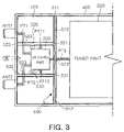
- FIG. 3 is a detailed configuration diagram illustrating the shielding wall 500 according to an exemplary embodiment of the present invention
- FIG. 4 is a partial perspective view illustrating a pattern-passing groove according to an exemplary embodiment of the present invention.
- the shielding wall 500 may be connected to grounds G 1 and G 2 of the switching part 200 via connection patterns PT 11 and PT 12 formed on the PCB 100 .
- the shielding wall 500 includes a first shielding wall 510 insulating the switching part 200 from the tuner part 300 , a second shielding wall 520 insulating the switching part 200 from the first input connector ANT 1 , and a third shielding wall 530 insulating the switching part 200 from the second input connector ANT 2 .
- a connection pattern PT 1 is a first connection pattern connecting the switching part 200 to the first input connector ANT 1
- a connection pattern PT 2 is a second connection pattern connecting the switching part 200 to the second input connector ANT 2
- a connection pattern PT 3 is an intermediate connection pattern connecting the switching part 200 to the tuner part 300 .
- the first shielding wall 510 includes a one end 511 connected to a lengthwise first inner surface of the chassis 400 ; an another end 512 connected to a second inner surface opposite to the first inner surface; and a pattern-passing groove 513 formed concavely in an area contacted with the PCT 100 , through which the intermediate connection pattern PT 3 connecting the switching part 200 to the tuner part 300 passes, to allow the intermediate connection pattern PT 3 to pass.
- the pattern-passing groove 513 provides a path for allowing the intermediate connection pattern PT 3 to pass without an electrical contact, thereby preventing an electrical connection between the intermediate connection pattern PT 3 and the first shielding wall 510 .
- the second shielding wall 520 includes a one end 521 connected to the first shielding wall 510 ; an another end 522 connected to a widthwise third inner surface of the chassis 400 , in which the third inner surface connects the first inner surface to the second inner surface of the chassis 400 ; and a pattern-passing groove 523 formed concavely in an area contacted with the PCT 100 , through which the first connection pattern PT 1 connecting the switching part 200 to the first input connector ANT 1 passes, to allow the first connection pattern PT 1 to pass.
- the pattern-passing groove 523 provides a path for allowing the first connection pattern PT 1 to pass without an electrical contact, thereby preventing an electrical connection between the first connection pattern PT 1 and the second shielding wall 520 .
- the second shielding wall 530 a one end 531 connected to the first shielding wall 510 ; an another end 532 connected to the third inner surface; and a pattern passing groove 533 formed concavely in an area contacted with the PCT 100 , through which the second connection pattern PT 2 connecting the switching part 200 to the second input connector ANT 2 passes, to allow the second connection pattern PT 2 to pass.
- the pattern-passing groove 533 provides a path for allowing the second connection pattern PT 2 to pass without an electrical contact, thereby preventing an electrical connection between the second connection pattern PT 2 and the third shielding wall 530 .
- FIG. 5 is a configuration diagram illustrating a tuner part according to an exemplary embodiment of the present invention.
- the tuner part 300 includes a data processor 310 analyzing the channel selection signal and the input selection signal included in the control data received via the control data pin P 2 , outputting a channel control signal according to the channel selection signal, and transmitting a switching signal to the switching part 200 according to the input selection signal; and a converter 320 down-converting an RF signal from the switching part 200 according to the channel control signal from the data processor 310 .
- control data pin P 2 may be formed of a clock signal pin CL for inputting a clock signal and a data pin DA for inputting the control data.
- the data processor 310 is connected to the switching part 200 via an individual connection pattern PT 4 .
- the first shielding wall 510 may further include a pattern-passing groove 514 concavely formed in an area contacted with the PCT 100 , through which the connection pattern PT 4 connecting the switching part 200 to the tuner part 300 passes.
- FIG. 6 is an external view illustrating a television tuning apparatus 3000 according to an exemplary embodiment of the present invention
- FIG. 7 is a cross-section cut along a line A-A′ shown in FIG. 6 to illustrate a first installation example of the television tuning apparatus of FIG. 6
- FIG. 8 is a cross-section cut along a line A-A′ shown in FIG. 6 to illustrate a second installation example of the television tuning apparatus of FIG. 6 .
- the chassis 400 includes a body chassis 410 coupled with the PCB 100 and covering sides of the PCB 100 to protect the sides of the PCB 100 ; a first cover chassis 420 coupled with the body chassis 410 and covering an exposed portion of a one surface of the PCB 100 to protect the one surface of the PCB 100 ; and a second cover chassis 430 coupled with the body chassis 410 and covering an exposed portion of another surface of the PCB 100 , the another surface opposite to the one surface, to protect the another surface of the PCB 100 .
- the body chassis 410 is coupled with an edge portion of the PCB 100 in the shape of a general square.
- the body chassis 410 is formed in a square-shaped frame structure including a plurality of coupling protrusions formed on a lower portion thereof to be inserted into a coupling groove formed on the edge portion of the PCB 100 to couple the PCB 100 with the body chassis 410 .
- a general coupler for coupling the PCB 100 with the body chassis may be employed.
- the switching part 200 may be formed on one surface of the PCB 100 and the tuner part 300 may be formed on the one surface together with the switching part 200 .
- the PCB 100 may be formed of a one-side substrate.
- the switching part 200 may be formed on one surface of the PCB 100 and the tuner part 300 may be formed on another surface of the PCB 100 .
- the PCB 100 may be formed of a double-sided substrate.
- the PCB 100 may be formed of a multi substrate.
- a portion of the first cover chassis 420 includes a plurality of touch pointers 421 .
- the touch pointers 421 may be formed to be contacted with the shielding wall 500 .
- FIG. 9 is a configuration diagram illustrating a television tuning apparatus 3000 according to an exemplary embodiment of the present invention.
- the apparatus 3000 may include a demodulating part 600 demodulating a signal from the tuner part 300 .
- the demodulating part 600 includes an analog demodulator 610 demodulating the first RF signal RF 1 and a digital demodulator 620 demodulating the second RF signal RF 2 .
- the first RF signal RF 1 is an RF signal for analog broadcasting and the second RF signal RF 2 is an RF signal for digital broadcasting.
- the apparatus 3000 may be employed by a television receiver.
- the television receiver will be described with reference to FIG. 10 .
- FIG. 10 is a block diagram illustrating a television receiver according to an exemplary embodiment of the present invention.
- the television receiver includes a power supply unit 1000 supplying a voltage for operation; a controller 2000 providing control data including a channel selection signal and an input selection signal; and the television tuning apparatus 3000 formed of one chassis, the apparatus 3000 receiving the voltage for operation from the power supply unit 1000 , and down-converting one of a first RF signal RF 1 and a second RF signal RF 2 according to the input selection signal included in the control data from the controller 2000 .
- the switching part 200 installed on the PCB 100 selects and outputs one of the first RF signal RF 1 and the second RF signal RF 2 to the tuner part 300 .
- the first RF signal RF 1 is inputted via the first input connector ANT 1 supported by the chassis 400 and the second RF signal RF 2 is inputted via the second input connector ANT 2 supported by the chassis 400 .
- the tuner part 300 down-converts an RF signal from the switching part 200 into an IF signal and outputs the IF signal.
- the chassis 400 covers the PCB 100 , the switching part 200 , and the tuner part 300 , the PCB 100 , the switching part 200 , and the tuner part 300 may be protected from an external impact. Also, since the chassis 400 is electrically connected to grounds of the switching part 200 and the tuner part 300 , an unnecessary signal inflow between the inside and the outside of the apparatus 3000 may be prevented.
- the shielding wall 500 connected to the chassis 400 shields the switching part 200 from a signal interference with at least one of other elements connected to the PCB 100 , thereby insulating the switching part 200 from the other elements connected to the PCB 100 .
- the apparatus 3000 may receive a switching signal via a switching terminal and provide the switching signal to the switching part 200 .
- the switching part 200 may select one of the first RF signal RF 1 and the second RF signal RF 2 according to the switching signal.
- the switching terminal may be formed of a pin connector PCON that will be described below.
- the apparatus 3000 receives a voltage for operation of the tuner part 300 via the power pin P 1 of the pin connector PCON and receives control data including a channel selection signal and an input selection signal for selecting one of the first RF signal RF 1 and the second RF signal RF 2 via the control data pin P 2 of the pin connector PCON.
- the control data is provided to the tuner part 300 .
- the apparatus 3000 outputs a signal from the tuner part 300 via the signal output pin P 3 of the pin connector PCON.
- the shielding wall 500 is connected to grounds G 1 and G 2 of the switching part 200 via connection patterns PT 11 and PT 12 formed on the PCB 100 , signal absorption of the shielding wall 500 is improved to strongly bypass a signal causing an interference to the ground, thereby more improving the shielding performance.
- the shielding wall 500 includes a first shielding wall 510 insulating the switching part 200 from the tuner part 300 , a second shielding wall 520 insulating the switching part 200 from the first input connector ANT 1 , and a third shielding wall 530 insulating the switching part 200 from the second input connector ANT 2
- the first shielding wall 510 shields the switching part 200 from the tuner part 300
- the second shielding wall 520 shields the switching part 200 from the first input connector ANT 1
- the third shielding wall 530 shields the switching part 200 from the second input connector ANT 2 .
- the data processor 310 analyzes a channel selection signal and an input selection signal included in the control data received via the control data pin P 2 , outputs a channel control signal according to the channel selection signal, and transmits a switching signal to the switching part 200 according to the input selection signal.
- the converter 320 down-converts an RF signal from the switching signal according to the channel control signal from the data processor 310 .
- the first RF signal RF 1 may correspond to an RF signal for analog broadcasting and the second RF signal RF 2 may correspond to an RF signal for digital broadcasting.
- the apparatus 3000 includes a demodulating part 600 including an analog demodulator 610 and a digital demodulator 620
- the analog demodulator 610 may demodulate the first RF signal RF 1 that is the RF signal for analog broadcasting
- the digital demodulator 620 may demodulate the second RF signal RF 2 that is the RF signal for digital broadcasting.
- the apparatus 3000 may be employed by a television receiver that will be described referring to FIG. 10 .
- a power supply unit 1000 may supply a voltage for operation to the apparatus 3000 via a pin connector PCON.
- the controller 2000 may transfer control data including a channel selection signal and an input selection signal to the apparatus 3000 .
- the apparatus 3000 may receive the voltage from the power supply unit 1000 and may select and down-convert one of the first RF signal RF 1 and the second RF signal RF 2 according to the input selection signal included in the control data transferred from the controller 2000 .
- an aspect of the present invention provides a single package television tuning apparatus including a switching part for selecting multi input and a tuner part installed together on one chassis and shielding the switching part form other elements to prevent a signal interference between the switching part and the other elements and to carry out size reduction and a low price and a television receiver including the apparatus.
Abstract
Description
Claims (46)
Applications Claiming Priority (6)
| Application Number | Priority Date | Filing Date | Title |
|---|---|---|---|
| KR20060053579 | 2006-06-14 | ||
| KR10-2006-0053579 | 2006-06-14 | ||
| KR10-2006-53579 | 2006-06-14 | ||
| KR1020070022094A KR100818477B1 (en) | 2006-06-14 | 2007-03-06 | Single package television tuning apparatus, and television receiver |
| KR10-2007-0022094 | 2007-03-06 | ||
| KR10-2007-22094 | 2007-03-06 |
Publications (2)
| Publication Number | Publication Date |
|---|---|
| US20070291182A1 US20070291182A1 (en) | 2007-12-20 |
| US7692520B2 true US7692520B2 (en) | 2010-04-06 |
Family
ID=38318859
Family Applications (1)
| Application Number | Title | Priority Date | Filing Date |
|---|---|---|---|
| US11/750,195 Expired - Fee Related US7692520B2 (en) | 2006-06-14 | 2007-05-17 | Single package television tuning apparatus and television receiver including the same |
Country Status (5)
| Country | Link |
|---|---|
| US (1) | US7692520B2 (en) |
| JP (1) | JP4665091B2 (en) |
| KR (1) | KR100818477B1 (en) |
| DE (1) | DE102007022637A1 (en) |
| GB (1) | GB2439176B (en) |
Cited By (2)
| Publication number | Priority date | Publication date | Assignee | Title |
|---|---|---|---|---|
| US8747121B1 (en) * | 2013-01-24 | 2014-06-10 | Cresta Technology Corporation | Television tuner module having a shielded housing mounted on an outer circuit board and having an inner circuit board with a tuner chip |
| US11395418B2 (en) * | 2017-11-28 | 2022-07-19 | Sony Semiconductor Solutions Corporation | Tuner module and receiving device |
Families Citing this family (6)
| Publication number | Priority date | Publication date | Assignee | Title |
|---|---|---|---|---|
| KR200449860Y1 (en) * | 2008-09-10 | 2010-08-16 | (주)한솔이십일 | Wideband Amplifier |
| KR101867846B1 (en) * | 2011-11-01 | 2018-06-19 | 삼성전자주식회사 | Television tuner module and Broadcast receiving apparatus having the same |
| CN102628934A (en) * | 2012-03-12 | 2012-08-08 | 东南大学 | 3mm wave band three-channel low noise integration receiving front-end |
| CN105791721B (en) * | 2012-11-22 | 2018-09-07 | 江苏华兴电子有限公司 | Tuner component with antenna isolator |
| CN103237188B (en) * | 2012-11-22 | 2016-05-04 | 江苏华兴电子有限公司 | Tuner assembly |
| CN105791720B (en) * | 2012-11-22 | 2018-09-07 | 江苏华兴电子有限公司 | Tuner component for the antenna isolator for ensuring high-frequency signal transmission quality |
Citations (4)
| Publication number | Priority date | Publication date | Assignee | Title |
|---|---|---|---|---|
| JPH02288513A (en) | 1989-04-28 | 1990-11-28 | Hitachi Ltd | Tuner demodulation unit |
| KR20040098094A (en) | 2003-05-13 | 2004-11-20 | 엘지이노텍 주식회사 | Sash shield method of rf switch built-in type tuner |
| KR20040099876A (en) | 2003-05-20 | 2004-12-02 | 삼성전자주식회사 | Tuner having 2RF spliter built-in |
| US20060038924A1 (en) * | 2004-08-19 | 2006-02-23 | Sharp Kabushiki Kaisha | Tuner employed to receive digital broadcast |
Family Cites Families (5)
| Publication number | Priority date | Publication date | Assignee | Title |
|---|---|---|---|---|
| JPS5840981U (en) * | 1981-09-09 | 1983-03-17 | アルプス電気株式会社 | Structure of high frequency equipment |
| JPH0669842A (en) * | 1992-08-21 | 1994-03-11 | Japan Radio Co Ltd | Diversity receiver |
| KR940008435A (en) * | 1992-09-16 | 1994-04-29 | 이종수 | Built-in tuner with wired / wireless broadcasting selector switch |
| JPH1084297A (en) * | 1996-09-09 | 1998-03-31 | Hitachi Media Electron:Kk | Receiving device |
| JP2001177424A (en) * | 1999-12-20 | 2001-06-29 | Sony Corp | Tuner unit |
-
2007
- 2007-03-06 KR KR1020070022094A patent/KR100818477B1/en not_active IP Right Cessation
- 2007-05-15 DE DE102007022637A patent/DE102007022637A1/en not_active Ceased
- 2007-05-17 US US11/750,195 patent/US7692520B2/en not_active Expired - Fee Related
- 2007-05-31 JP JP2007145817A patent/JP4665091B2/en not_active Expired - Fee Related
- 2007-06-07 GB GB0710889A patent/GB2439176B/en not_active Expired - Fee Related
Patent Citations (4)
| Publication number | Priority date | Publication date | Assignee | Title |
|---|---|---|---|---|
| JPH02288513A (en) | 1989-04-28 | 1990-11-28 | Hitachi Ltd | Tuner demodulation unit |
| KR20040098094A (en) | 2003-05-13 | 2004-11-20 | 엘지이노텍 주식회사 | Sash shield method of rf switch built-in type tuner |
| KR20040099876A (en) | 2003-05-20 | 2004-12-02 | 삼성전자주식회사 | Tuner having 2RF spliter built-in |
| US20060038924A1 (en) * | 2004-08-19 | 2006-02-23 | Sharp Kabushiki Kaisha | Tuner employed to receive digital broadcast |
Non-Patent Citations (2)
| Title |
|---|
| Korean Intellectual Property Office, Office Action mailed Dec. 13, 2007 and English Translation. |
| UK Intellectual Property Office Search Report mailed, Sep. 20, 2007 and English Translation. |
Cited By (2)
| Publication number | Priority date | Publication date | Assignee | Title |
|---|---|---|---|---|
| US8747121B1 (en) * | 2013-01-24 | 2014-06-10 | Cresta Technology Corporation | Television tuner module having a shielded housing mounted on an outer circuit board and having an inner circuit board with a tuner chip |
| US11395418B2 (en) * | 2017-11-28 | 2022-07-19 | Sony Semiconductor Solutions Corporation | Tuner module and receiving device |
Also Published As
| Publication number | Publication date |
|---|---|
| DE102007022637A1 (en) | 2007-12-27 |
| GB0710889D0 (en) | 2007-07-18 |
| KR20070119484A (en) | 2007-12-20 |
| KR100818477B1 (en) | 2008-04-02 |
| JP2007336535A (en) | 2007-12-27 |
| GB2439176B (en) | 2011-02-16 |
| JP4665091B2 (en) | 2011-04-06 |
| GB2439176A (en) | 2007-12-19 |
| US20070291182A1 (en) | 2007-12-20 |
Similar Documents
| Publication | Publication Date | Title |
|---|---|---|
| US7692520B2 (en) | Single package television tuning apparatus and television receiver including the same | |
| JP2663823B2 (en) | High frequency device | |
| KR100957257B1 (en) | Signal reception device and signal reception circuit | |
| CN102696285A (en) | Tuner module and receiver | |
| KR100610187B1 (en) | High-frequency receiving unit and high-frequency receiving method | |
| US7813708B2 (en) | Tuner module | |
| WO2015164445A1 (en) | Apparatus and method for controlling current in a device due to electrostatic discharge or surge event | |
| JP4669505B2 (en) | Shield case | |
| WO2009150411A1 (en) | Multifunctional device | |
| US20080273122A1 (en) | Reception system | |
| JP3940901B2 (en) | Tuner and receiver | |
| KR100755609B1 (en) | A set top box having direct connection for modules | |
| CN215499382U (en) | TV set-top box | |
| JP2010200129A (en) | Tuner | |
| JP4157835B2 (en) | Cable modem module device, cable modem device, and broadcast receiving device | |
| KR20220017148A (en) | Tuner module | |
| JP2005253019A (en) | Signal mixer | |
| JP2009111889A (en) | Tuner | |
| KR20060109643A (en) | Mobile communication terminal with assistant antenna apparatus | |
| JP2008035378A (en) | Small module and device for mobile usage with the same mounted thereon | |
| US20070149165A1 (en) | Board layout structure of digital broadcast receiving portion | |
| JP2011239004A (en) | High-frequency signal receiver | |
| JP2005354147A (en) | Television tuner | |
| KR20090030489A (en) | Tuner | |
| JP2001346184A (en) | Community reception device |
Legal Events
| Date | Code | Title | Description |
|---|---|---|---|
| AS | Assignment |
Owner name: SAMSUNG ELECTRO-MECHANICS CO., LTD., KOREA, REPUBL Free format text: ASSIGNMENT OF ASSIGNORS INTEREST;ASSIGNORS:KIM, BYUNG HYUK;LEE, KYO SANG;MUN, YOUNG HONG;AND OTHERS;REEL/FRAME:019310/0682 Effective date: 20070502 Owner name: SAMSUNG ELECTRO-MECHANICS CO., LTD.,KOREA, REPUBLI Free format text: ASSIGNMENT OF ASSIGNORS INTEREST;ASSIGNORS:KIM, BYUNG HYUK;LEE, KYO SANG;MUN, YOUNG HONG;AND OTHERS;REEL/FRAME:019310/0682 Effective date: 20070502 |
|
| FEPP | Fee payment procedure |
Free format text: PAYOR NUMBER ASSIGNED (ORIGINAL EVENT CODE: ASPN); ENTITY STATUS OF PATENT OWNER: LARGE ENTITY |
|
| FPAY | Fee payment |
Year of fee payment: 4 |
|
| AS | Assignment |
Owner name: SOLUM CO., LTD, KOREA, REPUBLIC OF Free format text: ASSIGNMENT OF ASSIGNORS INTEREST;ASSIGNOR:SAMSUNG ELECTRO-MECHANICS CO., LTD;REEL/FRAME:037438/0306 Effective date: 20151223 |
|
| FEPP | Fee payment procedure |
Free format text: MAINTENANCE FEE REMINDER MAILED (ORIGINAL EVENT CODE: REM.) |
|
| LAPS | Lapse for failure to pay maintenance fees |
Free format text: PATENT EXPIRED FOR FAILURE TO PAY MAINTENANCE FEES (ORIGINAL EVENT CODE: EXP.) |
|
| STCH | Information on status: patent discontinuation |
Free format text: PATENT EXPIRED DUE TO NONPAYMENT OF MAINTENANCE FEES UNDER 37 CFR 1.362 |
|
| FP | Lapsed due to failure to pay maintenance fee |
Effective date: 20180406 |