US7691783B2 - Transfer substrate, method for fabricating display device, and display device - Google Patents
Transfer substrate, method for fabricating display device, and display device Download PDFInfo
- Publication number
- US7691783B2 US7691783B2 US11/380,032 US38003206A US7691783B2 US 7691783 B2 US7691783 B2 US 7691783B2 US 38003206 A US38003206 A US 38003206A US 7691783 B2 US7691783 B2 US 7691783B2
- Authority
- US
- United States
- Prior art keywords
- transfer
- layer
- transfer substrate
- absorption region
- laser light
- Prior art date
- Legal status (The legal status is an assumption and is not a legal conclusion. Google has not performed a legal analysis and makes no representation as to the accuracy of the status listed.)
- Expired - Fee Related, expires
Links
Images


Classifications
-
- C—CHEMISTRY; METALLURGY
- C23—COATING METALLIC MATERIAL; COATING MATERIAL WITH METALLIC MATERIAL; CHEMICAL SURFACE TREATMENT; DIFFUSION TREATMENT OF METALLIC MATERIAL; COATING BY VACUUM EVAPORATION, BY SPUTTERING, BY ION IMPLANTATION OR BY CHEMICAL VAPOUR DEPOSITION, IN GENERAL; INHIBITING CORROSION OF METALLIC MATERIAL OR INCRUSTATION IN GENERAL
- C23C—COATING METALLIC MATERIAL; COATING MATERIAL WITH METALLIC MATERIAL; SURFACE TREATMENT OF METALLIC MATERIAL BY DIFFUSION INTO THE SURFACE, BY CHEMICAL CONVERSION OR SUBSTITUTION; COATING BY VACUUM EVAPORATION, BY SPUTTERING, BY ION IMPLANTATION OR BY CHEMICAL VAPOUR DEPOSITION, IN GENERAL
- C23C14/00—Coating by vacuum evaporation, by sputtering or by ion implantation of the coating forming material
- C23C14/04—Coating on selected surface areas, e.g. using masks
- C23C14/048—Coating on selected surface areas, e.g. using masks using irradiation by energy or particles
-
- H—ELECTRICITY
- H10—SEMICONDUCTOR DEVICES; ELECTRIC SOLID-STATE DEVICES NOT OTHERWISE PROVIDED FOR
- H10K—ORGANIC ELECTRIC SOLID-STATE DEVICES
- H10K71/00—Manufacture or treatment specially adapted for the organic devices covered by this subclass
- H10K71/10—Deposition of organic active material
- H10K71/18—Deposition of organic active material using non-liquid printing techniques, e.g. thermal transfer printing from a donor sheet
-
- H—ELECTRICITY
- H10—SEMICONDUCTOR DEVICES; ELECTRIC SOLID-STATE DEVICES NOT OTHERWISE PROVIDED FOR
- H10K—ORGANIC ELECTRIC SOLID-STATE DEVICES
- H10K71/00—Manufacture or treatment specially adapted for the organic devices covered by this subclass
- H10K71/20—Changing the shape of the active layer in the devices, e.g. patterning
-
- H—ELECTRICITY
- H10—SEMICONDUCTOR DEVICES; ELECTRIC SOLID-STATE DEVICES NOT OTHERWISE PROVIDED FOR
- H10K—ORGANIC ELECTRIC SOLID-STATE DEVICES
- H10K71/00—Manufacture or treatment specially adapted for the organic devices covered by this subclass
- H10K71/40—Thermal treatment, e.g. annealing in the presence of a solvent vapour
- H10K71/421—Thermal treatment, e.g. annealing in the presence of a solvent vapour using coherent electromagnetic radiation, e.g. laser annealing
-
- H—ELECTRICITY
- H10—SEMICONDUCTOR DEVICES; ELECTRIC SOLID-STATE DEVICES NOT OTHERWISE PROVIDED FOR
- H10K—ORGANIC ELECTRIC SOLID-STATE DEVICES
- H10K71/00—Manufacture or treatment specially adapted for the organic devices covered by this subclass
-
- Y—GENERAL TAGGING OF NEW TECHNOLOGICAL DEVELOPMENTS; GENERAL TAGGING OF CROSS-SECTIONAL TECHNOLOGIES SPANNING OVER SEVERAL SECTIONS OF THE IPC; TECHNICAL SUBJECTS COVERED BY FORMER USPC CROSS-REFERENCE ART COLLECTIONS [XRACs] AND DIGESTS
- Y10—TECHNICAL SUBJECTS COVERED BY FORMER USPC
- Y10S—TECHNICAL SUBJECTS COVERED BY FORMER USPC CROSS-REFERENCE ART COLLECTIONS [XRACs] AND DIGESTS
- Y10S430/00—Radiation imagery chemistry: process, composition, or product thereof
- Y10S430/146—Laser beam
-
- Y—GENERAL TAGGING OF NEW TECHNOLOGICAL DEVELOPMENTS; GENERAL TAGGING OF CROSS-SECTIONAL TECHNOLOGIES SPANNING OVER SEVERAL SECTIONS OF THE IPC; TECHNICAL SUBJECTS COVERED BY FORMER USPC CROSS-REFERENCE ART COLLECTIONS [XRACs] AND DIGESTS
- Y10—TECHNICAL SUBJECTS COVERED BY FORMER USPC
- Y10T—TECHNICAL SUBJECTS COVERED BY FORMER US CLASSIFICATION
- Y10T428/00—Stock material or miscellaneous articles
- Y10T428/24—Structurally defined web or sheet [e.g., overall dimension, etc.]
- Y10T428/24802—Discontinuous or differential coating, impregnation or bond [e.g., artwork, printing, retouched photograph, etc.]
-
- Y—GENERAL TAGGING OF NEW TECHNOLOGICAL DEVELOPMENTS; GENERAL TAGGING OF CROSS-SECTIONAL TECHNOLOGIES SPANNING OVER SEVERAL SECTIONS OF THE IPC; TECHNICAL SUBJECTS COVERED BY FORMER USPC CROSS-REFERENCE ART COLLECTIONS [XRACs] AND DIGESTS
- Y10—TECHNICAL SUBJECTS COVERED BY FORMER USPC
- Y10T—TECHNICAL SUBJECTS COVERED BY FORMER US CLASSIFICATION
- Y10T428/00—Stock material or miscellaneous articles
- Y10T428/31504—Composite [nonstructural laminate]
Definitions
- the present invention contains subject matter related to Japanese Patent Application JP 2005-128909 filed in the Japanese Patent Office on Apr. 27, 2005, the entire contents of which are incorporated herein by reference.
- the present invention relates to a luminescent material transfer substrate for transferring a transfer layer including at least a luminescent layer by sublimation to a target object, a method for fabricating a display device using the transfer substrate, and a display device fabricated using the transfer substrate. More particularly, the invention relates to a method for fabricating a display device that includes organic electroluminescent elements and a display device that includes organic electroluminescent elements.
- Organic EL elements using electroluminescence (hereinafter referred to as “EL”) of organic materials have been receiving attention as light-emitting elements capable of achieving high-luminance light emission at low-voltage DC drive.
- luminescent elements each emitting light of red (R), green (G), or blue (B) are arrayed on a substrate, organic layers each including at least a luminescent layer of any of these colors are formed.
- a transfer method i.e., thermal transfer method
- an energy source heat source
- a thin film layer to be transferred is formed by vapor deposition, spin coating, printing, or the like on a transfer substrate, and after the thin film layer is attached to a substrate on which film formation is to be performed, energy such as laser light or heat is applied from the transfer substrate side. Subsequently, an organic layer on the transfer substrate is separated with the thin film layer being left partially or entirely, and thus the organic layer formed on the transfer substrate is transferred onto the substrate.
- the advantage of the thermal transfer method is that patterning is not particularly required when a transfer layer is formed on a transfer substrate, and an organic layer is merely formed on the entire surface of the transfer substrate.
- a laser is preferably used from the standpoint that high energy can be supplied locally. Furthermore, when scanning is performed with a laser beam having a reduced diameter, it is possible to form a line pattern very accurately, and higher definition is enabled.
- Japanese Patent Nos. 2918037 and 3175733 each disclose a method in which a member having low thermal conductivity and a member having high thermal conductivity represented by copper (Cu) are patterned in advance onto a transfer substrate, and a desired organic layer is transferred using a laser, a heat bar, or the like as the heat source.
- a member having low thermal conductivity and a member having high thermal conductivity represented by copper (Cu) are patterned in advance onto a transfer substrate, and a desired organic layer is transferred using a laser, a heat bar, or the like as the heat source.
- a luminescent material such as an organic EL element
- a transfer substrate includes a support base which transmits laser light with a predetermined wavelength, a photothermal conversion layer provided on the support base, and a transfer layer provided on the photothermal conversion layer, the transfer layer including at least a luminescent layer, wherein the photothermal conversion layer is composed of a first material and a second material having different absorptances with respect to the laser light.
- the first material forms a high-absorption region that absorbs the laser light and generates heat required for sublimation of the transfer layer
- the second material forms a low-absorption region that reflects and blocks the laser light so as not to generate heat required for sublimation of the transfer layer.
- a method for fabricating a display device includes the steps of placing a transfer substrate so as to face a device-forming substrate, the transfer substrate being prepared by forming a transfer layer including at least a luminescent layer on a support base provided with a photothermal conversion layer composed of a first material and a second material having different absorptances with respect to laser light, and selectively transferring a portion of the transfer layer corresponding to the first material having higher absorptance onto the device-forming substrate by irradiating the transfer substrate with laser light.
- the device-forming substrate onto which the transfer layer is to be transferred and the transfer substrate on which the transfer layer has been formed are positioned so as to face each other, and the transfer substrate is irradiated with laser light.
- the transfer substrate is irradiated with laser light.
- the difference in absorptance with respect to laser light between the two materials constituting the photothermal conversion layer provided on the transfer substrate is used in the step of transferring the transfer layer.
- laser light is applied to the entire surface of the transfer layer, it is possible to selectively transfer a portion of the transfer layer onto the device-forming substrate correspondingly to the high-absorption region.
- FIG. 1 is a schematic plan view of a display device according to an embodiment of the present invention.
- FIG. 2 is a schematic cross-sectional view of an organic EL element
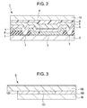
- FIG. 3 is a schematic cross-sectional view of a transfer substrate according to the embodiment of the present invention.
- FIG. 4 is a graph showing an example of relationship between wavelength and reflectance
- FIG. 5 is a schematic cross-sectional view illustrating a transfer step in a method for fabricating a display device according to the embodiment of the present invention
- FIG. 6 is a schematic cross-sectional view illustrating a structure of a functional layer.
- FIG. 7 is a schematic cross-sectional view of another example of a transfer substrate.
- FIG. 1 is a schematic view of a display device according to an embodiment of the present invention.
- An organic EL element 1 is provided correspondingly to each pixel a.
- the organic EL element 1 includes a lower electrode 3 , a functional layer 4 , and an upper common electrode 5 provided in that order on a substrate 2 .
- a protective film 8 is provided over the upper common electrode 5 , and a glass substrate 10 is attached thereto through an UV curable resin 9 .
- auxiliary wiring 7 when an auxiliary wiring 7 is provided between the pixels a, the functional layer 4 above the auxiliary wiring 7 is removed so that the upper common electrode 5 and the auxiliary wiring 7 are brought into contact and connected with each other.
- auxiliary wiring 7 By applying a voltage to the upper common electrode 5 using the auxiliary wiring 7 , it is possible to suppress the voltage drop and in-plane variation in voltage distribution in the upper common electrode 5 , and to maintain the luminescent luminance of the organic EL element 1 in each pixel a.
- the functional layer 4 used in the organic EL element 1 includes, as shown in FIG. 6 which is a schematic cross-sectional view, a hole injection layer 41 , a hole transport layer 42 , a luminescent layer 43 , an electron transport layer 44 , and an electron injection layer 45 provided in that order on the lower electrode 3 .
- FIG. 3 is a schematic cross-sectional view of a transfer substrate according to the embodiment of the present invention.
- a transfer substrate S includes a support base 100 which transmits laser light with a predetermined wavelength, a transfer layer 40 provided on the support base 100 , and two types of regions provided on the support base 100 and having different absorptances with respect to laser light (i.e., a low-reflection layer 101 and a high-reflection layer 102 ).
- the low-reflection layer 101 absorbs laser light and generates heat required for sublimation of the transfer layer 40 and corresponds to a high-absorption region that can efficiently absorb laser light.
- the high-reflection layer 102 reflects and blocks laser light so as not to generate heat required for sublimation of the transfer layer 40 and corresponds to a low-absorption region that does not substantially absorb laser light.
- description will be made on the assumption that the high-absorption region corresponds to the low-reflection layer 101 and the low-absorption region corresponds to the high-reflection layer 102 .
- the low-reflection layer 101 and the high-reflection layer 102 are provided between the support base 100 and the transfer layer 40 .
- the low-reflection layer 101 and the high-reflection layer 102 may be provided on a surface of the support base 100 opposite to the surface on which the transfer layer 40 is provided.
- the support base 100 for example, a glass substrate or the like that satisfactorily transmits laser light with a wavelength of 800 to 1,000 nm is used.
- a glass substrate By using a glass substrate, alignment with a device-forming substrate can be performed reliably, and when the transfer layer 40 remaining after sublimation is reused, handling is facilitated.
- patterning may be performed using ordinary photolithography.
- the materials for the low-reflection layer 101 and the high-reflection layer 102 are chosen so that a satisfactory selection ratio is obtained between the materials such that when the same amount of laser light is applied to these layers, the low-reflection layer 101 causes sublimation of the transfer layer 40 and the high-reflection layer 102 does not cause sublimation of the transfer layer 40 .
- FIG. 4 is a graph showing an example of relationship between wavelength and reflectance.
- the laser light with a wavelength of 800 nm (0.8 ⁇ m) to 1,000 nm (1.0 ⁇ m) which is used in the embodiment of the present invention Cr and Mo have low reflectance and Au and Ag have high reflectance.
- the difference in reflectance between the low-reflection layer 101 and the high-reflection layer 102 is preferably 20% to 50%. With such a difference in reflectance, when the same amount of laser light is applied, a selection ratio can be obtained such that the low-reflection layer 101 causes sublimation of the transfer layer 40 and the high-reflection layer 102 does not cause sublimation of the transfer layer 40 .
- the low-reflection layer 101 a material selected from metals, such as molybdenum (Mo) and chromium (Co), and alloys containing these metals is used.
- a material selected from metals such as gold (Au), silver (Ag), copper (Cu), and aluminum (Al), and alloys containing these metals (e.g., APC: Ag—Pd—Cu alloy) is used.
- the low-reflection layer 101 and the high-reflection layer 102 may be each composed of a metal. Alternatively, they may be each composed of carbon or a resin as long as a satisfactory selection ratio is obtained because of the difference in reflectance and the materials themselves are not sublimated by irradiation of laser light.
- the low-reflection layer 101 and the high-reflection layer 102 are each composed of a metal, a difference in thermal conduction may occur depending on the materials. However, in this embodiment of the present invention, since the low-reflection layer 101 and the high-reflection layer 102 are each formed with an extremely small thickness, the influence of thermal conduction does not occur.
- the thickness of each of the low-reflection layer 101 and the high-reflection layer 102 is larger than the thickness at which the transmittance of laser light is substantially zero and is a thickness at which patterning can be easily performed and the influence of thermal diffusion does not occur, and the thickness is preferably 100 to 200 nm, and more preferably about 100 nm.
- the transfer substrate S it is necessary to form the low-reflection layer 101 and the high-reflection layer 102 without openings between the layers so that leakage of laser light does not occur even if the entire surface is irradiated with the laser light. Furthermore, since the transfer layer 40 is formed on the support base 100 with the low-reflection layer 101 and the high-reflection layer 102 therebetween, preferably, the low-reflection layer 101 and the high-reflection layer 102 are formed at substantially the same thickness. Thereby, the transfer layer 40 can be formed uniformly (evenly), and transfer can be performed with high accuracy.
- a transfer substrate S may be produced by performing patterning of a low-reflection layer 101 only for a portion to be transferred, and then forming a high-reflection layer 102 entirely thereon.
- a step occurs in the transfer layer 40 at the portion to be transferred.
- the transfer substrate S can be produced by patterning of the low-reflection layer 101 only, and thus the production process can be greatly simplified.
- a lower electrode 3 is formed on a substrate 2 .
- the lower electrode 3 is used as an anode or a cathode.
- the lower electrode 3 is composed of a highly reflective material.
- the display device is of a transmissive type, the lower electrode 3 is formed to be transparent.
- the display device is of a top emission type, and the lower electrode 3 is used as an anode.
- the lower electrode 3 is composed of an electrically conductive material having high reflectance, such as silver (Ag), aluminum (Al), chromium (Cr), iron (Fe), cobalt (Co), nickel (Ni), copper (Cu), tantalum (Ta), tungsten (W), platinum (Pt), gold (Au), or an alloy thereof.
- the lower electrode 3 is composed of an electrically conductive material having a small work function.
- an electrically conductive material which may be used include alloys of an active metal, such as lithium (Li), magnesium (Mg), or calcium (Ca), and a metal, such as silver (Ag), aluminum (Al), or indium (In), and laminates of these metals.
- a structure may be employed in which a layer composed of a compound of an active metal, such as Li, Mg, or Ca, and a halogen, such as fluorine or bromine, oxygen or the like is interposed between the lower electrode 3 and the functional layer 4 .
- the lower electrode 3 is composed of an electrically conductive material having high transmittance, such as Indium-Tin-Oxide (ITO) or Indium-Zinc-Oxide (IZO).
- ITO Indium-Tin-Oxide
- IZO Indium-Zinc-Oxide
- the lower electrode 3 is composed of an electrically conductive material having a small work function and high transmittance.
- the insulating film 6 is, for example, composed of an organic insulating material, such as a polyimide or a photoresist, or an inorganic insulating material, such as silicon oxide.
- a functional layer 4 is formed on the lower electrode 3 in each pixel a sequentially.
- the functional layer 4 is formed so as to completely cover the exposed surface of the lower electrode 3 .
- a hole injection layer 41 , a hole transport layer 42 , and a luminescent layer 43 , and as necessary, an electron transport layer 44 , and an electron injection layer 45 are deposited in that order on the lower electrode 3 .
- the functional layer 4 A specific example of the functional layer 4 will be described below.
- layers (common layers) other than the luminescent layer 43 are solidly formed, and in each element, an independent luminescent layer 43 is formed by laser thermal transfer using any of three colors: red (R), green (G), or blue (B).
- R red
- G green
- B blue
- the present invention is also effective with respect to a device in which common layers are provided in a discrete form, a method in which common layers are also formed by laser thermal transfer according to the embodiment of the present invention, and a tandem organic EL element in which units (luminescent units) of a functional layer including a luminescent layer 43 are stacked.
- the term “luminescent unit” refers to a component constituting a known organic EL element excluding an anode and a cathode, i.e., a single luminescent layer or a plurality of layers including a luminescent layer, an electron injection layer, an electron transport layer, a hole injection layer, a hole transport layer, etc., and is a unit for generating light corresponding to a single color or multiple colors.
- m-MTDATA 4,4,4-tris(3-methylphenylphenylamino)triphenylamine
- ⁇ -NPD 4,4-bis(N-1-naphthyl-N-phenylamino)biphenyl
- the material is not limited thereto, and for example, a hole transport material, such as a benzidine derivative, a styrylamine derivative, a triphenylmethane derivative, or a hydrazone derivative, may be used.
- the individual organic layers for example, the hole injection layer and the hole transport layer, each may have a layered structure including a plurality of layers.
- a low-reflection layer 101 corresponding to a transfer region is formed using Mo and a high-reflection layer 102 corresponding to a non-transfer region is formed using APC (Ag—Pd—Cu), each at a thickness of 200 nm and by patterning using ordinary lithography on a support base 100 composed of glass.
- a transfer layer (luminescent material) 40 is formed thereon, and a transfer substrate S is thereby prepared.
- a luminescent layer 43 is formed at a thickness of 25 nm using the luminescent material transfer substrate S.
- the difference in reflectance between APC and Mo is 40% or more, which is sufficient for selective transfer.
- the material which may be used for the high-reflection layer 102 include Ag, Al, Cu, and alloys thereof, and examples of the material which may be used for the low-reflection layer 101 include Mo, Cr, and alloys thereof.
- the materials are not limited thereto, and the materials are chosen so as to produce a difference in reflectance that enables selective transfer.
- FIG. 1 in order to perform color display using a structure in which a plurality of pixels a arrayed in a matrix on a substrate emit light of R, G, and B, different light-emitting organic compounds are used for luminescent layers for R, G, and B. That is, at least three transfer substrates S are required.
- a red luminescent layer includes, for example, a red luminescent material, and at least one of a hole transport material, an electron transport material, and a hole and electron transport material.
- the red luminescent material may be fluorescent or phosphorescent.
- the red luminescent layer has a thickness of about 30 nm and is composed of a material prepared by mixing 30% by weight of 2,6-bis[(4′-methoxydiphenylamino)styryl]-1,5-dicyanonaphthalene (BSN) with ADN.
- a green luminescent layer includes, for example, a green luminescent material, and at least one of a hole transport material, an electron transport material, and a hole and electron transport material.
- the green luminescent material may be fluorescent or phosphorescent.
- the green luminescent layer has a thickness of about 30 nm and is composed of a material prepared by mixing 5% by weight of coumarin 6 with ADN.
- a blue luminescent layer includes, for example, a blue luminescent material, and at least one of a hole transport material, an electron transport material, and a hole and electron transport material.
- the blue luminescent material may be fluorescent or phosphorescent.
- the blue luminescent layer has a thickness of about 30 nm and is composed of a material prepared by mixing 2.5% by weight of 4,4′-bis[2- ⁇ 4-(N,N-diphenylamino)phenyl ⁇ vinyl]biphenyl (DPAVBi) with ADN.
- the substrate 2 on which layers up to the hole transport layer 42 have been deposited is positioned in a transfer relationship with the transfer substrate S according to this embodiment on which the transfer layer 40 has been deposited. Both substrates are in close contact with each other. However, since the insulating film 6 for isolating pixels is thicker than the transfer layer 40 which has been deposited, the organic layers are only in close proximity to each other but not in close contact with each other. In this step, preferably, a vacuum environment is produced. Thereby, adhesion between the substrates is increased, and pattern accuracy in transfer is improved.
- infrared laser light of 800 nm is applied toward the transfer substrate S so as to be absorbed by the light absorption region composed of the low-reflection layer 101 , and using heat generated therefrom, the transfer layer 40 including the luminescent layer 43 is transferred onto the hole transport layer 42 which has been deposited on the substrate 2 .
- the low-reflection layer 101 and the high-reflection layer 102 are formed without openings on the transfer substrate S. Therefore, for example, even if the entire surface of the transfer substrate S is irradiated with laser light, the laser light can be reflected by the region other than the low-reflection layer 101 which is formed correspondingly to the portion to be transferred and the laser light is absorbed only by the low-reflection layer 101 . As a result, a portion of the transfer layer 40 corresponding thereto only can be sublimated. Consequently, highly accurate transfer can be accomplished by a simple device configuration without providing a complex driving member for a laser head or an alignment mechanism.
- the thermal transfer described above is performed repeatedly using different transfer substrates S for RGB three colors.
- the whole process is carried out in a vacuum. Thereby, degradation of the device can be prevented and adhesion between the substrates can be improved.
- thermal transfer in a vacuum is preferred.
- thermal separation in a vacuum laser separation can be performed with lower energy, and an adverse thermal effect on adjacent pixels can be reduced.
- an electron transport layer 44 is solidly formed over the entire surface of the display area.
- the electron transport layer 44 has a thickness of 20 nm and is composed of 8-hydroxyquinoline aluminum (Alq3).
- LiF is vacuum vapor deposited as an electron injection layer 45 at a thickness of about 0.3 nm (vapor deposition rate: 0.01 nm/sec), and then MgAg is vacuum vapor deposited as an upper common electrode 5 at a thickness of 10 nm.
- the upper common electrode 5 is used as an anode or a cathode.
- the upper common electrode 5 is formed to be transparent or translucent.
- the upper common electrode 5 is composed of a highly reflective material.
- the upper common electrode 5 is formed by a deposition method in which energy of particles deposited is small to such an extent that does not adversely affect the underlayer, for example, by a vapor deposition method or a chemical vapor deposition (CVD) method.
- the upper common electrode 5 is continuously formed in the same apparatus as that used for forming the functional layer 4 without exposing the functional layer 4 to the air. Thereby, the functional layer 4 is prevented from being degraded by the moisture in the air.
- the upper common electrode 5 is used as a cathode.
- the upper common electrode 5 is formed to be transparent using a material having a small work function so that electrons can be effectively injected into the functional layer 4 .
- the upper common electrode 5 is preferably formed as a metal thin film by a deposition method in which energy of particles deposited is small, such as a vapor deposition method.
- the upper common electrode 5 is composed of an electrically conductive material having a small work function and high reflectance.
- the upper common electrode 5 is composed of an electrically conductive material having high reflectance.
- a protective film 8 which is insulating or electrically conductive is provided over the transparent upper common electrode 5 composed of a metal thin film.
- the protective film 8 is formed by a deposition method in which energy of particles deposited is small to such an extent that does not adversely affect the underlayer, for example, by a vapor deposition method or a chemical vapor deposition (CVD) method.
- the protective film 8 is continuously formed in the same apparatus as that used for the formation of the upper common electrode 5 without exposing the upper common electrode 5 to the air. Thereby, the functional layer 4 is prevented from being degraded by the moisture and oxygen in the air.
- the protective film 8 is formed with a sufficient thickness using a material having low water permeability and low water absorption in order to prevent moisture from reaching the functional layer 4 .
- the protective film 8 is composed of a material that transmits light generated in the functional layer 4 , and for example, a transmittance of about 80% is ensured.
- the protective film 8 is composed of an insulating material. That is, the insulating protective film 8 is directly formed on the single-layered upper common electrode 5 composed of a metal thin film.
- Examples of the material that can be preferably used for the protective film 8 include inorganic amorphous, insulating materials, such as amorphous silicon ( ⁇ -Si), amorphous silicon carbide ( ⁇ -SiC), amorphous silicon nitride ( ⁇ -Si 1-x N x ), and amorphous carbon ( ⁇ -C). Since such inorganic amorphous, insulating materials do not form grains, they have low water permeability, and thus can form a satisfactory protective film 8 .
- inorganic amorphous, insulating materials such as amorphous silicon ( ⁇ -Si), amorphous silicon carbide ( ⁇ -SiC), amorphous silicon nitride ( ⁇ -Si 1-x N x ), and amorphous carbon ( ⁇ -C). Since such inorganic amorphous, insulating materials do not form grains, they have low water permeability, and thus can form a satisfactory protective film 8 .
- the protective film 8 is formed at a thickness of 2 to 3 ⁇ m by a CVD method.
- deposition is performed at normal temperature.
- the deposition conditions are set such that the stress on the film is minimized.
- the protective film 8 is composed of an electrically conductive material
- a transparent electrically conductive material such as ITO or IXO, is used.
- a glass substrate 10 is fixed on the protective film 8 , as necessary, with an UV curable resin 9 therebetween. Thereby, the display device is completed.
- the transfer layer including the luminescent layer is thermally transferred using the transfer substrate S according to the embodiment of the present invention. It may be possible to perform thermal transfer using the transfer substrate S according to the embodiment of the present invention when any of the organic layers other than the luminescent layer is formed.
- the high-reflection layer 102 has been explained as an example of the low-absorption region that does not substantially absorb laser light in the photothermal conversion layer.
- the low-absorption layer a transparent layer that transmits laser light, i.e., that does not substantially absorb laser light not by reflection but by transmission.
Landscapes
- Engineering & Computer Science (AREA)
- Chemical & Material Sciences (AREA)
- Manufacturing & Machinery (AREA)
- Toxicology (AREA)
- Optics & Photonics (AREA)
- Health & Medical Sciences (AREA)
- Physics & Mathematics (AREA)
- Electromagnetism (AREA)
- Chemical Kinetics & Catalysis (AREA)
- Materials Engineering (AREA)
- Mechanical Engineering (AREA)
- Metallurgy (AREA)
- Organic Chemistry (AREA)
- Electroluminescent Light Sources (AREA)
- Physical Vapour Deposition (AREA)
Abstract
Description
Claims (23)
Applications Claiming Priority (2)
| Application Number | Priority Date | Filing Date | Title |
|---|---|---|---|
| JP2005128909A JP2006309995A (en) | 2005-04-27 | 2005-04-27 | Transfer substrate, display device manufacturing method, and display device |
| JPP2005-128909 | 2005-04-27 |
Publications (2)
| Publication Number | Publication Date |
|---|---|
| US20060246240A1 US20060246240A1 (en) | 2006-11-02 |
| US7691783B2 true US7691783B2 (en) | 2010-04-06 |
Family
ID=37234775
Family Applications (1)
| Application Number | Title | Priority Date | Filing Date |
|---|---|---|---|
| US11/380,032 Expired - Fee Related US7691783B2 (en) | 2005-04-27 | 2006-04-25 | Transfer substrate, method for fabricating display device, and display device |
Country Status (2)
| Country | Link |
|---|---|
| US (1) | US7691783B2 (en) |
| JP (1) | JP2006309995A (en) |
Cited By (9)
| Publication number | Priority date | Publication date | Assignee | Title |
|---|---|---|---|---|
| US20080268135A1 (en) * | 2007-04-27 | 2008-10-30 | Semiconductor Energy Laboratory Co.,Ltd. | Manufacturing method of light-emitting device |
| US20090142510A1 (en) * | 2007-11-29 | 2009-06-04 | Semiconductor Energy Laboratory Co., Ltd. | Evaporation Donor Substrate and Method for Manufacturing Light-Emitting Device |
| US20090226631A1 (en) * | 2008-03-07 | 2009-09-10 | Semiconductor Energy Laboratory Co., Ltd. | Method for Forming Film and Method for Manufacturing Light Emitting Device |
| US20090297694A1 (en) * | 2008-05-29 | 2009-12-03 | Semiconductor Energy Laboratory Co., Ltd. | Deposition Method and Method for Manufacturing Light-Emitting Device |
| US20110193124A1 (en) * | 2008-04-14 | 2011-08-11 | Semiconductor Energy Laboratory Co., Ltd. | Deposition Substrate and Method for Manufacturing Light-Emitting Device |
| US20120012883A1 (en) * | 2009-04-22 | 2012-01-19 | Tomoya Aoyama | Method for manufacturing light-emitting device and film formation substrate |
| US8815352B2 (en) | 2010-03-18 | 2014-08-26 | Semiconductor Energy Laboratory Co., Ltd. | Film forming method and method for manufacturing film-formation substrate |
| US8900675B2 (en) | 2010-03-18 | 2014-12-02 | Semiconductor Energy Laboratory Co., Ltd. | Deposition method and method for manufacturing deposition substrate |
| US8951816B2 (en) | 2010-03-18 | 2015-02-10 | Semiconductor Energy Laboratory Co., Ltd. | Film forming method |
Families Citing this family (37)
| Publication number | Priority date | Publication date | Assignee | Title |
|---|---|---|---|---|
| KR101563237B1 (en) * | 2007-06-01 | 2015-10-26 | 가부시키가이샤 한도오따이 에네루기 켄큐쇼 | Manufacturing apparatus and manufacturing method of light-emitting device |
| KR20090028413A (en) * | 2007-09-13 | 2009-03-18 | 가부시키가이샤 한도오따이 에네루기 켄큐쇼 | Method of manufacturing light emitting device and substrate for deposition |
| KR20090041316A (en) * | 2007-10-23 | 2009-04-28 | 가부시키가이샤 한도오따이 에네루기 켄큐쇼 | Film formation method and manufacturing method of light emitting device |
| US8153201B2 (en) | 2007-10-23 | 2012-04-10 | Semiconductor Energy Laboratory Co., Ltd. | Method of manufacturing light-emitting device, and evaporation donor substrate |
| KR20090041314A (en) * | 2007-10-23 | 2009-04-28 | 가부시키가이샤 한도오따이 에네루기 켄큐쇼 | Manufacturing method of substrate and light emitting device for deposition |
| KR101689519B1 (en) * | 2007-12-26 | 2016-12-26 | 가부시키가이샤 한도오따이 에네루기 켄큐쇼 | Evaporation donor substrate, method for manufacturing the same, and method for manufacturing light-emitting device |
| US8080811B2 (en) * | 2007-12-28 | 2011-12-20 | Semiconductor Energy Laboratory Co., Ltd. | Method for manufacturing evaporation donor substrate and light-emitting device |
| KR101307549B1 (en) * | 2007-12-31 | 2013-09-12 | 엘지디스플레이 주식회사 | Manufacturing Method for Organic Light Emitting Display |
| JP2009175198A (en) * | 2008-01-21 | 2009-08-06 | Sony Corp | El display panel and electronic apparatus |
| WO2009099002A1 (en) | 2008-02-04 | 2009-08-13 | Semiconductor Energy Laboratory Co., Ltd. | Deposition method and method for manufacturing light-emitting device |
| JP2009231277A (en) * | 2008-02-29 | 2009-10-08 | Semiconductor Energy Lab Co Ltd | Manufacturing apparatus |
| WO2009107548A1 (en) | 2008-02-29 | 2009-09-03 | Semiconductor Energy Laboratory Co., Ltd. | Deposition method and manufacturing method of light-emitting device |
| JP5416987B2 (en) * | 2008-02-29 | 2014-02-12 | 株式会社半導体エネルギー研究所 | Film forming method and light emitting device manufacturing method |
| JP5367415B2 (en) * | 2008-03-06 | 2013-12-11 | 株式会社半導体エネルギー研究所 | Method for manufacturing light emitting device and substrate for film formation |
| JP5238544B2 (en) * | 2008-03-07 | 2013-07-17 | 株式会社半導体エネルギー研究所 | Film forming method and light emitting device manufacturing method |
| US8182863B2 (en) | 2008-03-17 | 2012-05-22 | Semiconductor Energy Laboratory Co., Ltd. | Deposition method and manufacturing method of light-emitting device |
| US7993945B2 (en) | 2008-04-11 | 2011-08-09 | Semiconductor Energy Laboratory Co., Ltd. | Method for manufacturing light-emitting device |
| US8409672B2 (en) | 2008-04-24 | 2013-04-02 | Semiconductor Energy Laboratory Co., Ltd. | Method of manufacturing evaporation donor substrate and method of manufacturing light-emitting device |
| JP5159689B2 (en) * | 2008-04-25 | 2013-03-06 | 株式会社半導体エネルギー研究所 | Method for manufacturing light emitting device |
| US7919340B2 (en) | 2008-06-04 | 2011-04-05 | Semiconductor Energy Laboratory Co., Ltd. | Method for manufacturing light-emitting device |
| US8574709B2 (en) | 2008-07-21 | 2013-11-05 | Semiconductor Energy Laboratory Co., Ltd. | Deposition donor substrate and method for manufacturing light-emitting device |
| JP5469950B2 (en) * | 2008-08-08 | 2014-04-16 | 株式会社半導体エネルギー研究所 | Method for manufacturing light emitting device |
| JP2010080439A (en) * | 2008-09-01 | 2010-04-08 | Toray Ind Inc | Donor substrate for transfer, and method for manufacturing device using the same |
| US8486736B2 (en) * | 2008-10-20 | 2013-07-16 | Semiconductor Energy Laboratory Co., Ltd. | Method for manufacturing light-emitting device |
| JP5291607B2 (en) | 2008-12-15 | 2013-09-18 | 株式会社半導体エネルギー研究所 | Method for manufacturing light emitting device |
| JP5438313B2 (en) * | 2008-12-23 | 2014-03-12 | 株式会社半導体エネルギー研究所 | Deposition method |
| JP2010153051A (en) * | 2008-12-24 | 2010-07-08 | Sony Corp | Transfer substrate and method for manufacturing display |
| JP5143064B2 (en) * | 2009-03-17 | 2013-02-13 | 株式会社半導体エネルギー研究所 | Method for manufacturing light emitting device |
| JP5111427B2 (en) * | 2009-04-16 | 2013-01-09 | 株式会社半導体エネルギー研究所 | Film forming substrate and film forming method |
| KR20140102518A (en) * | 2013-02-14 | 2014-08-22 | 삼성디스플레이 주식회사 | Donor film, method for fabricating the same and method for fabricating organic light emitting display using the same |
| KR20140118534A (en) * | 2013-03-29 | 2014-10-08 | 삼성디스플레이 주식회사 | Donor substrate and method for forming transfer pattern using the same |
| KR20150012530A (en) * | 2013-07-25 | 2015-02-04 | 삼성디스플레이 주식회사 | Donor substrate for trnasfer and manufacturing method of organic light emitting diode display |
| KR20150135720A (en) * | 2014-05-23 | 2015-12-03 | 삼성디스플레이 주식회사 | Donor mask and method for manufacturing organic light-emitting display apparatus |
| KR102180647B1 (en) * | 2014-09-03 | 2020-11-23 | 삼성디스플레이 주식회사 | Optical mask |
| JP6660603B2 (en) * | 2017-12-05 | 2020-03-11 | パナソニックIpマネジメント株式会社 | Sputtering method |
| US11021788B2 (en) | 2017-12-05 | 2021-06-01 | Panasonic Intellectual Property Management Co., Ltd. | Sputtering method |
| TWI793026B (en) * | 2022-05-27 | 2023-02-11 | 友達光電股份有限公司 | Pixel array substrate |
Citations (1)
| Publication number | Priority date | Publication date | Assignee | Title |
|---|---|---|---|---|
| JP3175733B2 (en) | 1998-06-17 | 2001-06-11 | 日本電気株式会社 | Manufacturing method of organic EL device |
Family Cites Families (4)
| Publication number | Priority date | Publication date | Assignee | Title |
|---|---|---|---|---|
| JP3428598B2 (en) * | 1993-10-08 | 2003-07-22 | ソニー株式会社 | Light absorber |
| US5688551A (en) * | 1995-11-13 | 1997-11-18 | Eastman Kodak Company | Method of forming an organic electroluminescent display panel |
| US5937272A (en) * | 1997-06-06 | 1999-08-10 | Eastman Kodak Company | Patterned organic layers in a full-color organic electroluminescent display array on a thin film transistor array substrate |
| KR100667069B1 (en) * | 2004-10-19 | 2007-01-10 | 삼성에스디아이 주식회사 | Method of manufacturing a donor substrate and an organic light emitting display device using the same |
-
2005
- 2005-04-27 JP JP2005128909A patent/JP2006309995A/en active Pending
-
2006
- 2006-04-25 US US11/380,032 patent/US7691783B2/en not_active Expired - Fee Related
Patent Citations (1)
| Publication number | Priority date | Publication date | Assignee | Title |
|---|---|---|---|---|
| JP3175733B2 (en) | 1998-06-17 | 2001-06-11 | 日本電気株式会社 | Manufacturing method of organic EL device |
Cited By (15)
| Publication number | Priority date | Publication date | Assignee | Title |
|---|---|---|---|---|
| US20080268135A1 (en) * | 2007-04-27 | 2008-10-30 | Semiconductor Energy Laboratory Co.,Ltd. | Manufacturing method of light-emitting device |
| US8367152B2 (en) | 2007-04-27 | 2013-02-05 | Semiconductor Energy Laboratory Co., Ltd. | Manufacturing method of light-emitting device |
| US8425974B2 (en) | 2007-11-29 | 2013-04-23 | Semiconductor Energy Laboratory Co., Ltd. | Evaporation donor substrate and method for manufacturing light-emitting device |
| US20090142510A1 (en) * | 2007-11-29 | 2009-06-04 | Semiconductor Energy Laboratory Co., Ltd. | Evaporation Donor Substrate and Method for Manufacturing Light-Emitting Device |
| US20090226631A1 (en) * | 2008-03-07 | 2009-09-10 | Semiconductor Energy Laboratory Co., Ltd. | Method for Forming Film and Method for Manufacturing Light Emitting Device |
| US8277902B2 (en) | 2008-03-07 | 2012-10-02 | Semiconductor Energy Laboratory Co., Ltd. | Method for forming film and method for manufacturing light emitting device |
| US20110193124A1 (en) * | 2008-04-14 | 2011-08-11 | Semiconductor Energy Laboratory Co., Ltd. | Deposition Substrate and Method for Manufacturing Light-Emitting Device |
| US8653543B2 (en) | 2008-04-14 | 2014-02-18 | Semiconductor Energy Laboratory Co., Ltd. | Deposition substrate and method for manufacturing light-emitting device |
| US20090297694A1 (en) * | 2008-05-29 | 2009-12-03 | Semiconductor Energy Laboratory Co., Ltd. | Deposition Method and Method for Manufacturing Light-Emitting Device |
| US8802185B2 (en) | 2008-05-29 | 2014-08-12 | Semiconductor Energy Laboratory Co., Ltd. | Deposition method and method for manufacturing light-emitting device |
| US8618568B2 (en) * | 2009-04-22 | 2013-12-31 | Semiconductor Energy Laboratory Co., Ltd. | Method for manufacturing light-emitting device and film formation substrate |
| US20120012883A1 (en) * | 2009-04-22 | 2012-01-19 | Tomoya Aoyama | Method for manufacturing light-emitting device and film formation substrate |
| US8815352B2 (en) | 2010-03-18 | 2014-08-26 | Semiconductor Energy Laboratory Co., Ltd. | Film forming method and method for manufacturing film-formation substrate |
| US8900675B2 (en) | 2010-03-18 | 2014-12-02 | Semiconductor Energy Laboratory Co., Ltd. | Deposition method and method for manufacturing deposition substrate |
| US8951816B2 (en) | 2010-03-18 | 2015-02-10 | Semiconductor Energy Laboratory Co., Ltd. | Film forming method |
Also Published As
| Publication number | Publication date |
|---|---|
| JP2006309995A (en) | 2006-11-09 |
| US20060246240A1 (en) | 2006-11-02 |
Similar Documents
| Publication | Publication Date | Title |
|---|---|---|
| US7691783B2 (en) | Transfer substrate, method for fabricating display device, and display device | |
| US9209233B2 (en) | Method for manufacturing display and display | |
| US7887987B2 (en) | Transfer substrate, transfer method, and method of manufacturing display device | |
| US7723735B2 (en) | Display device and a method of manufacturing the same | |
| KR101355413B1 (en) | Red organic light emitting element and display device provided with same, donor substrate and transfer method using same, method of manufacturing display device, and system of manufacturing display device | |
| US7632714B2 (en) | Method for manufacturing a display device | |
| US7993806B2 (en) | Transfer substrate, and fabrication process of organic electroluminescent devices | |
| JP4957375B2 (en) | Organic EL display device manufacturing equipment | |
| US20090038550A1 (en) | Evaporation source, manufacturing method of the same and manufacturing method of an organic el display device | |
| JP2006286493A (en) | Display element, display device, and display element manufacturing method | |
| US7553602B2 (en) | Transfer substrate, transfer method, and organic electroluminescent device manufacturing method | |
| JP4793071B2 (en) | Display device and manufacturing method of display device | |
| JP2010027210A (en) | Manufacturing method of light-emitting element, and light-emitting element | |
| JP2008288017A (en) | Manufacturing method of organic EL display device | |
| JP2006309955A (en) | Method for manufacturing organic electroluminescent device and organic electroluminescent device | |
| JP2012060174A (en) | Display apparatus | |
| JP2011243593A (en) | Donor substrate, transfer method using the same, display manufacturing method, and display manufacturing system | |
| JP2010287388A (en) | Method for manufacturing organic electroluminescent device |
Legal Events
| Date | Code | Title | Description |
|---|---|---|---|
| AS | Assignment |
Owner name: SONY CORPORATION,JAPAN Free format text: ASSIGNMENT OF ASSIGNORS INTEREST;ASSIGNORS:MATSUDA, EISUKE;NISHIGUCHI, MASAO;REEL/FRAME:017522/0358 Effective date: 20060406 Owner name: SONY CORPORATION, JAPAN Free format text: ASSIGNMENT OF ASSIGNORS INTEREST;ASSIGNORS:MATSUDA, EISUKE;NISHIGUCHI, MASAO;REEL/FRAME:017522/0358 Effective date: 20060406 |
|
| FEPP | Fee payment procedure |
Free format text: PAYOR NUMBER ASSIGNED (ORIGINAL EVENT CODE: ASPN); ENTITY STATUS OF PATENT OWNER: LARGE ENTITY |
|
| FPAY | Fee payment |
Year of fee payment: 4 |
|
| AS | Assignment |
Owner name: JOLED INC., JAPAN Free format text: ASSIGNMENT OF ASSIGNORS INTEREST;ASSIGNOR:SONY CORPORATION;REEL/FRAME:036106/0355 Effective date: 20150618 |
|
| FEPP | Fee payment procedure |
Free format text: MAINTENANCE FEE REMINDER MAILED (ORIGINAL EVENT CODE: REM.) |
|
| LAPS | Lapse for failure to pay maintenance fees |
Free format text: PATENT EXPIRED FOR FAILURE TO PAY MAINTENANCE FEES (ORIGINAL EVENT CODE: EXP.) |
|
| STCH | Information on status: patent discontinuation |
Free format text: PATENT EXPIRED DUE TO NONPAYMENT OF MAINTENANCE FEES UNDER 37 CFR 1.362 |
|
| FP | Lapsed due to failure to pay maintenance fee |
Effective date: 20180406 |