US7687724B2 - Circuitized substrate with internal resistor, method of making said circuitized substrate, and electrical assembly utilizing said circuitized substrate - Google Patents
Circuitized substrate with internal resistor, method of making said circuitized substrate, and electrical assembly utilizing said circuitized substrate Download PDFInfo
- Publication number
- US7687724B2 US7687724B2 US11/806,685 US80668507A US7687724B2 US 7687724 B2 US7687724 B2 US 7687724B2 US 80668507 A US80668507 A US 80668507A US 7687724 B2 US7687724 B2 US 7687724B2
- Authority
- US
- United States
- Prior art keywords
- electrical
- dielectric layer
- layer
- substrate
- resistor
- Prior art date
- Legal status (The legal status is an assumption and is not a legal conclusion. Google has not performed a legal analysis and makes no representation as to the accuracy of the status listed.)
- Expired - Fee Related, expires
Links
Images


Classifications
-
- H—ELECTRICITY
- H05—ELECTRIC TECHNIQUES NOT OTHERWISE PROVIDED FOR
- H05K—PRINTED CIRCUITS; CASINGS OR CONSTRUCTIONAL DETAILS OF ELECTRIC APPARATUS; MANUFACTURE OF ASSEMBLAGES OF ELECTRICAL COMPONENTS
- H05K1/00—Printed circuits
- H05K1/02—Details
- H05K1/09—Use of materials for the conductive, e.g. metallic pattern
- H05K1/092—Dispersed materials, e.g. conductive pastes or inks
- H05K1/095—Dispersed materials, e.g. conductive pastes or inks for polymer thick films, i.e. having a permanent organic polymeric binder
-
- H—ELECTRICITY
- H05—ELECTRIC TECHNIQUES NOT OTHERWISE PROVIDED FOR
- H05K—PRINTED CIRCUITS; CASINGS OR CONSTRUCTIONAL DETAILS OF ELECTRIC APPARATUS; MANUFACTURE OF ASSEMBLAGES OF ELECTRICAL COMPONENTS
- H05K1/00—Printed circuits
- H05K1/16—Printed circuits incorporating printed electric components, e.g. printed resistors, capacitors or inductors
- H05K1/167—Printed circuits incorporating printed electric components, e.g. printed resistors, capacitors or inductors incorporating printed resistors
-
- H—ELECTRICITY
- H05—ELECTRIC TECHNIQUES NOT OTHERWISE PROVIDED FOR
- H05K—PRINTED CIRCUITS; CASINGS OR CONSTRUCTIONAL DETAILS OF ELECTRIC APPARATUS; MANUFACTURE OF ASSEMBLAGES OF ELECTRICAL COMPONENTS
- H05K1/00—Printed circuits
- H05K1/02—Details
- H05K1/11—Printed elements for providing electric connections to or between printed circuits
- H05K1/115—Via connections; Lands around holes or via connections
- H05K1/116—Lands, clearance holes or other lay-out details concerning the surrounding of a via
-
- H—ELECTRICITY
- H05—ELECTRIC TECHNIQUES NOT OTHERWISE PROVIDED FOR
- H05K—PRINTED CIRCUITS; CASINGS OR CONSTRUCTIONAL DETAILS OF ELECTRIC APPARATUS; MANUFACTURE OF ASSEMBLAGES OF ELECTRICAL COMPONENTS
- H05K2203/00—Indexing scheme relating to apparatus or processes for manufacturing printed circuits covered by H05K3/00
- H05K2203/05—Patterning and lithography; Masks; Details of resist
- H05K2203/0562—Details of resist
- H05K2203/0568—Resist used for applying paste, ink or powder
-
- H—ELECTRICITY
- H05—ELECTRIC TECHNIQUES NOT OTHERWISE PROVIDED FOR
- H05K—PRINTED CIRCUITS; CASINGS OR CONSTRUCTIONAL DETAILS OF ELECTRIC APPARATUS; MANUFACTURE OF ASSEMBLAGES OF ELECTRICAL COMPONENTS
- H05K3/00—Apparatus or processes for manufacturing printed circuits
- H05K3/40—Forming printed elements for providing electric connections to or between printed circuits
- H05K3/42—Plated through-holes or plated via connections
- H05K3/429—Plated through-holes specially for multilayer circuits, e.g. having connections to inner circuit layers
-
- Y—GENERAL TAGGING OF NEW TECHNOLOGICAL DEVELOPMENTS; GENERAL TAGGING OF CROSS-SECTIONAL TECHNOLOGIES SPANNING OVER SEVERAL SECTIONS OF THE IPC; TECHNICAL SUBJECTS COVERED BY FORMER USPC CROSS-REFERENCE ART COLLECTIONS [XRACs] AND DIGESTS
- Y10—TECHNICAL SUBJECTS COVERED BY FORMER USPC
- Y10T—TECHNICAL SUBJECTS COVERED BY FORMER US CLASSIFICATION
- Y10T29/00—Metal working
- Y10T29/49—Method of mechanical manufacture
- Y10T29/49002—Electrical device making
- Y10T29/49117—Conductor or circuit manufacturing
- Y10T29/49124—On flat or curved insulated base, e.g., printed circuit, etc.
- Y10T29/49155—Manufacturing circuit on or in base
- Y10T29/49165—Manufacturing circuit on or in base by forming conductive walled aperture in base
Definitions
- the present invention relates to providing resistors within circuitized substrates such as printed circuit boards, chip carriers and the like, and more specifically to a method for doing so and to products including such internal resistors as part thereof. Even more particularly, the invention relates to such methodologies and products wherein the internal resistors are formed using powder materials having nano-particles or micro-particles or combinations of both as part thereof.
- Non-Flaking Capacitor Material, Capacitive Substrate Having An Internal Capacitor Therein Including Said Non-Flaking Capacitor Material And Method Of Making A Capacitor Member For Use In A Capacitive Substrate there is defined a capacitor material including a thermosetting resin (e.g., epoxy resin), a high molecular mass flexibilizer (e.g., phenoxy resin), and a quantity of nano-particles of a ferroelectric ceramic material (e.g., barium titanate), the capacitor material not including continuous or semi-continuous fibers (e.g., fiberglass) as part thereof.
- a thermosetting resin e.g., epoxy resin
- a high molecular mass flexibilizer e.g., phenoxy resin
- a ferroelectric ceramic material e.g., barium titanate
- the material is adapted for being positioned in layer form on a first conductor member and heated to a predetermined temperature whereupon the material will not possess any substantial flaking characteristics.
- a second conductor member may then be positioned on the material to form a capacitor member, which then may be incorporated within a substrate to form a capacitive substrate.
- Electrical components may be positioned on the substrate and capacitively coupled to the internal capacitor.
- a method of making an information handling system including such substrates is also provided.
- epoxy novolac resin and a phenoxy resin are mixed together with barium titanate (BaTiO 3 ) powder and propylene glycol monomethyl ether acetate and methyl ethyl ketone and ball milled for three days.
- a 2.5 micron thin film of this mixed composite was then deposited on a copper substrate and dried at approximately 140 degrees C. for three minutes in an oven to remove residual organic solvents. This was followed by curing in an oven at 190 degrees C. for two hours.
- a second electrical conductor was then formed using a sputtering operation atop the cured film using a mask normally used for such sputtering operations.
- a circuitized substrate which includes a conductive paste for providing electrical connections.
- the paste in one embodiment, includes a binder component and at least one metallic component including micro-particles.
- the paste in another embodiment, includes the binder and a plurality of nano-wires. Selected ones of the micro-particles or nano-wires include a layer of solder thereon.
- a method of making such a substrate is also provided, as are an electrical assembly and information handling system adapter for having such a substrate as part thereof.
- epoxy novolac resin and a phenoxy resin are mixed together with barium titanate (BaTiO 3 ) powder and propylene glycol monomethyl ether acetate and methyl ethyl ketone and ball milled for three days.
- a 2.5 micron thin film of this mixed composite was deposited on a copper substrate and dried at approximately 140 degrees C. for three minutes in an oven to remove residual organic solvents. This was followed by curing in an oven at 190 degrees C. for two hours.
- a second electrical conductor was then formed using a sputtering operation atop the cured film using a mask normally used for such sputtering operations.
- the material will include the polymer resin and nano-powders, with the nano-powders comprising at least one metal coated ceramic and/or at least one oxide coated metal component.
- a circuitized substrate adapted for using such a material and resistor therein and a method of making such a substrate are also provided.
- An electrical assembly (substrate and at least one electrical component) and an information handling system (e.g., personal computer) are also provided.
- a circuitized substrate adapted for using such a material and capacitor therein and a method of making such a substrate are also provided.
- An electrical assembly substrate and at least one electrical component
- an information handling system e.g., personal computer
- an electrical assembly which includes a circuitized substrate comprised of an organic dielectric material having a first electrically conductive pattern thereon. At least part of the dielectric layer and pattern form the first, base portion of an organic memory device, the remaining portion being a second, polymer layer formed over the part of the pattern and a second conductive circuit formed on the polymer layer. A second dielectric layer if formed over the second conductive circuit and first circuit pattern to enclose the organic memory device.
- the device is electrically coupled to a first electrical component through the second dielectric layer and this first electrical component is electrically coupled to a second electrical component.
- a method of making the electrical assembly is also provided, as is an information handling system adapted for using one or more such electrical assemblies as part thereof. Ser. No. 10/900,386 is now U.S. Pat. No. 7,045,897.
- circuitized substrate comprised of at least one layer of dielectric material having an electrically conductive pattern thereon. At least part of the pattern is used as the first layer of an organic memory device which further includes at least a second dielectric layer over the pattern and a second pattern aligned with respect to the lower part for achieving several points of contact to thus form the device.
- the substrate is preferably combined with other dielectric-circuit layered assemblies to form a multilayered substrate on which can be positioned discrete electronic components (e.g., a logic chip) coupled to the internal memory device to work in combination therewith.
- An electrical assembly capable of using the substrate is also provided, as is an information handling system adapted for using one or more such electrical assemblies as part thereof.
- PCBs Printed circuit boards
- chip carriers and the like
- circuitized substrates typically are constructed in laminate form in which several layers of dielectric material and conductive material (laminates) are bonded together using relatively high temperature and pressure lamination processes.
- the conductive layers typically of thin copper or copper alloy, are usually used in the formed substrate for providing electrical connections to and among various devices located on the surface of the substrate, examples of such devices being integrated circuits (semiconductor chips) and discrete passive devices, such as capacitors, resistors, inductors, and the like.
- the discrete passive devices occupy a relatively high percentage of the surface area of the completed substrate, which is undesirable from a future design aspect because of the increased need and demand for miniaturization in today's substrates and products containing same art.
- substrate surface area also often referred to as “real estate”
- passive devices are in such a configuration, these are often referred to collectively and individually as integral passive devices or the like, meaning that the functions are integrated into the singular component. Because of such external positioning, these components still utilize, albeit less than if in singular form, board “real estate.”
- a capacitor or resistor designed for disposition within (e.g., between selected layers) a substrate may thus be referred to as an embedded integral passive component, or, more simply, an embedded resistor or capacitor.
- Such a capacitor thus provides internal capacitance while a resistor provides internal resistance.
- the result of this internal positioning is that it is unnecessary to also position such devices externally on the PCB's outer surface(s), thus saving valuable PCB surface area.
- a wiring board provided with a resistor
- the board comprises an insulating substrate having a surface, wiring patterns formed on the surface, the wiring patterns including first and second electrodes spaced from each other by a certain distance, a first resistor (horizontal type resistor) formed on the surface, the first resistor having respective ends connected with the first and second electrodes, respectively, the wiring patterns further including a third electrode, occupying a first plane area on the surface, a second resistor (vertical type resistor) formed on the third electrode, a fourth electrode formed on the second resistor, and the second resistor, the fourth electrode being located in a second plane area within the first plane area.
- a resistive film for use in a potentiometer.
- the film is in contact with a movable wiper.
- the film includes a cured polymer resin and a cured thermosetting resin.
- Conductive particles of carbon black and graphite are dispersed in the film.
- the conductive particles cause the resins to be electrically resistive.
- Carbon nano-particles are also dispersed in the film. The nano-particles increase the wear resistance of the resistive film and reduce electrical noise as the wiper moves across the film.
- a polymer solution is made by mixing 10-20 wt. percent of a polymer and 0-10 wt.
- thermosetting resin in 60-80 wt. percent N-methyl pyrrolidone, based upon the total composition.
- the polymer is mixed with both the conductive and nano-particles to form a paste with a fine particle size.
- surfactants and rheological additives may be added if desired to modify the properties of the resistive composition.
- the particle size range and viscosity of the paste is monitored to get a resistive paste suitable for application in position sensors.
- the milling time and milling quantity on the ball mill determines the final particle distribution, size and resulting rheology.
- PCB printed circuit board
- the PCB includes a first layer having first and second surfaces, with an above-board device (e.g., an ASIC chip) mounted thereon.
- the PCB includes a second layer having third and fourth surfaces.
- One of the surfaces can include a recessed portion for securely holding an interstitial component.
- a “via”, electrically connecting the PCB layers, is also coupled to a lead of the interstitial component.
- the described interstitial components include components such as diodes, transistors, resistors, capacitors, thermocouples, and the like.
- the interstitial component is a resistor having a similar size to a “0402” resistor (manufactured by Rohm Co.), which has a thickness of about 0.014 inches.
- Composites having dielectric constants greater than about 74 to about 150 are also mentioned in this patent. Also mentioned are embedded capacitors with capacitance densities of at least 25 nF/cm.sup.2, preferably at least 35 nF/cm.sup.2, most preferably 50 nF/cm.sup.2.
- the capacitor includes at least one internal conductive layer, two additional conductor layers added on opposite sides of the internal conductor, and inorganic dielectric material (preferably an oxide layer on the second conductor layer's outer surfaces or a suitable dielectric material such as barium titanate applied to the second conductor layers). Further, the capacitor includes outer conductor layers atop the inorganic dielectric material, thus forming a parallel capacitor between the internal and added conductive layers and the outer conductors.
- inorganic dielectric material preferably an oxide layer on the second conductor layer's outer surfaces or a suitable dielectric material such as barium titanate applied to the second conductor layers.
- a method for forming a patterned layer of resistive material in electrical contact with a layer of electrically conducting material comprises a metal conductive layer, an intermediate layer formed of material which is degradable by a chemical etchant, and a layer of resistive material of sufficient porosity such that the chemical etchant for the intermediate layer may seep through the resistive material and chemically degrade the intermediate layer so that the resistive material may be ablated from the conductive layer wherever the intermediate layer is chemically degraded.
- a patterned photo-resist layer is formed on the resistive material layer.
- the resistive material layer is exposed to the chemical etchant for the intermediate layer so that the etchant seeps through the porous resistive material layer and degrades the intermediate layer. Then, portions of the resistive material layer are ablated away wherever the intermediate layer has been degraded.
- the hybrid capacitor includes a low inductance, parallel plate capacitor which is embedded within the package and electrically connected to a second source of off-chip capacitance.
- the parallel plate capacitor is disposed underneath a die, and includes a top conductive layer, a bottom conductive layer, and a thin dielectric layer that electrically isolates the top and bottom layers.
- the second source of off-chip capacitance is a set of self-aligned via capacitors, and/or one or more discrete capacitors, and/or an additional parallel plate capacitor.
- Each of the self-aligned via capacitors is embedded within the package, and has an inner conductor and an outer conductor.
- the inner conductor is electrically connected to either the top or bottom conductive layer, and the outer conductor is electrically connected to the other conductive layer.
- the discrete capacitors are electrically connected to contacts from the conductive layers to the surface of the package.
- one of the conductive layers of the low inductance parallel plate capacitor provides a ground plane, while the other conductive layer provides a power plane.
- resistive materials are homogeneous mixtures of metals, such as platinum, and dielectric materials, such as silica or alumina. Even minor amounts of dielectric material admixed with a metal significantly increase the resistance of the metal.
- the resistive material is deposited on the insulating substrate by combustion chemical vapor deposition (CCVD). In the case of zero valence metals and dielectric material, the homogeneous mixture is achieved by co-deposition of the metal and dielectric material by CCVD.
- substantially any metal-based resistor material can be etched away.
- a layer of resistive material may be covered with a patterned resist, e.g., an exposed and developed photo-resist, and exposed portions of the underlying layer of resistive material etched away.
- This patent also describes the formation of thin layer resistors including the insulating substrate, discrete patches of a layer of resistive material, and conductive material in electrical contact with spaced-apart locations on the patches of resistive material layer, such conductive material providing for electrical connection of the resistive material patches with electronic circuitry.
- Such structures of insulating material, resistive material, and conductive material may be formed by selective etching procedures.
- the capacitor includes at least one internal conductive layer, two additional conductor layers added on opposite sides of the internal conductor, and inorganic dielectric material (preferably an oxide layer on the second conductor layer's outer surfaces or a suitable dielectric material such as barium titanate applied to the second conductor layers). Further, the capacitor includes outer conductor layers atop the inorganic dielectric material, thus forming a parallel capacitor between the internal and added conductive layers and the outer conductors.
- inorganic dielectric material preferably an oxide layer on the second conductor layer's outer surfaces or a suitable dielectric material such as barium titanate applied to the second conductor layers.
- the method also includes positioning a chip on the second side with a chip pad of the chip being aligned with the chip via, and patterning connection metallization on selected portions of the first side of the interconnect layer and in the via so as to extend to the second side metallized portion and to the chip pad.
- About the chip is molded a “substrate” or other dielectric material.
- a flexible, high dielectric constant polyimide film composed of either a single layer of an adhesive thermoplastic polyimide film or a multilayer polyimide film having adhesive thermoplastic polyimide film layers bonded to one or both sides of the film and having dispersed in at least one of the polyimide layers from 4 to 85 weight % of a ferroelectric ceramic filler, such as barium titanate or polyimide-coated barium titanate, and having a dielectric constant of from 4 to 60.
- the high dielectric constant polyimide film can be used in electronic circuitry and electronic components such as multilayer printed circuits, flexible circuits, semiconductor packaging and buried (internal) film capacitors
- a card structure which includes an internal three dimensional array of implanted semiconductor chips.
- the card structure includes a power core and a plurality of chip cores.
- Each chip core is joined to the power core on opposite surfaces of the power core, and each chip core includes a compensator core having a two dimensional array of chip wells.
- Each chip well allows for a respective one of the semiconductor chips to be implanted therein.
- a compliant dielectric material is disposed on the major surfaces of the compensator core except at the bottoms of the chip wells.
- the compliant dielectric material has a low dielectric constant and has a thermal coefficient of expansion compatible with those of the semiconductor chips and the compensator core, so that thermal expansion stability with the chips and the compensator core is maintained.
- a PCB which includes a high capacitance power distribution core, the manufacture of which is compatible with standard printed circuit board assembly technology.
- the high capacitance core consists of a ground plane and a power plane separated by a planar element having a high dielectric constant.
- the high dielectric constant material is typically glass fiber impregnated with a bonding material, such as epoxy resin loaded with a ferroelectric ceramic substance having a high dielectric constant.
- the ferroelectric ceramic substance is typically a nano-powder combined with an epoxy bonding material.
- the resulting capacitance of the power distribution core is sufficient to totally eliminate the need for decoupling capacitors on a PCB.
- Use of pre-fired and ground ceramic nano-powders in the dielectric layer poses obstacles for the formation of thru-holes (conductive holes permitting electronic communication between conductive layers of a PCB), however.
- Pre-fired and ground ceramic nano-powder particles have a typical dimension in the range of 500-20,000 nanometers (nm). Furthermore, the particle distribution in this range is generally rather broad, meaning that there could be a 10,000 nm particle alongside a 500 nm particle.
- the distribution within the dielectric layer of particles of different size often presents major obstacles to thru-hole formation where the thru-holes are of extremely small diameter, also referred to in the industry as micro-vias due to the presence of the larger particles.
- Another problem associated with pre-fired ceramic nano-powders is the ability for the dielectric layer to withstand substantial voltage without breakdown occurring across the layer.
- capacitance layers within a PCB are expected to withstand at least 300 volts (V) in order to qualify as a reliable component for PCB construction.
- V volts
- the presence of the comparatively larger ceramic particles in pre-fired ceramic nano-powders within a capacitance layer prevents extremely thin layers from being used because the boundaries of contiguous large particles provide a path for voltage breakdown. This is even further undesirable because, as indicated by the equation cited above, greater planar capacitance may also be achieved by reducing the thickness of the dielectric layer. The thickness is thus limited by the size of the particles therein.
- each memory core comprises a copper-invar-copper (CIC) thermal conductor plane having a two dimensional array of chip well locations on each side of the plane.
- CIC copper-invar-copper
- PTFE Polytetrafluoroethylene
- Each power core comprises at least one CIC electrical conductor plane and PTFE covering the major surfaces of the electrical conductor plane. Provision is made for providing electrical connection pathways and cooling pathways along vertical as well as horizontal planes internal to the card structure.
- dielectric powders which have been used in internal conductive structures such as mentioned in some of the above patents are known to be produced by a high-temperature, solid-state reaction of a mixture of the appropriate stoichiometric amounts of oxides or oxide precursors (e.g., carbonates, hydroxides or nitrates) of barium, calcium, titanium, and the like.
- oxides or oxide precursors e.g., carbonates, hydroxides or nitrates
- the reactants are wet-milled to accomplish a desired final mixture.
- the resulting slurry is dried and fired at elevated temperatures, sometimes as high as 1,300 degrees Celsius (C), to attain the desired solid state reactions. Thereafter, the fired product is milled to produce a powder.
- C 1,300 degrees Celsius
- the pre-fired and ground dielectric formulations produced by solid phase reactions are acceptable for many electrical applications, these suffer from several disadvantages.
- the milling step may serve as a source of contaminants, which can adversely affect electrical properties.
- the milled product may consist of irregularly shaped fractured aggregates which are often too large in size and possess a wide particle size distribution, 500-20,000 nm. Consequently, films produced using these powders are limited to thicknesses greater than the size of the largest particle.
- powder suspensions or composites produced using pre-fired ground ceramic powders must be used immediately after dispersion, due to the high sedimentation rates associated with large particles.
- the present invention is particularly directed to substantially eliminating many of such discontinuities by the provision of an internal resistor material as part of the internal circuit structure. By doing so, the invention is able to reduce capacitance and increase high frequency resistance at strategic locations within the circuit, thus improving system performance. It is believed that an invention possessing such features, as well as others discernible from the teachings herein, will constitute a significant advancement in the art.
- a method of making a circuitized substrate having circuitry including a resistor as part thereof comprising the steps of providing a first dielectric layer, forming a first electrical conductor on the first dielectric layer, forming an opening within the first electrical conductor, positioning a quantity of resistor material within the opening, forming a second dielectric layer substantially over the quantity of resistor material within the opening, forming a second electrical conductor on the second dielectric layer, and forming an electrical connection between the second and first electrical conductors, the quantity of resistor material serving to substantially reduce the capacitance between the electrical conductors and increase the high frequency resistance in the electrical connection between the electrical conductors.
- a circuitized substrate comprising a first dielectric layer, a first electrical conductor positioned on the first dielectric layer and including an opening therein, a quantity of resistor material within the opening, a second dielectric layer positioned substantially over the quantity of resistor material, a second electrical conductor positioned on the second dielectric layer, and an electrical connection between the second and first electrical conductors, the quantity of resistor material serving to substantially reduce the capacitance between the first and second electrical conductors and increase the high frequency resistance in the electrical connection between the first and second electrical conductors.
- an electrical assembly comprising a circuitized substrate including a first dielectric layer, a first electrical conductor positioned on the first dielectric layer and including an opening therein, a quantity of resistor material within the opening, a second dielectric layer positioned substantially over the quantity of resistor material, a second electrical conductor positioned on the second dielectric layer, and an electrical connection between the second and first electrical conductors, the quantity of resistor material serving to substantially reduce the capacitance between the first and second electrical conductors and increase the high frequency resistance in the electrical connection between the first and second electrical conductors, and at least one electrical component positioned on and electrically coupled to the circuitized substrate.
- FIGS. 1-7 are much enlarged, side elevational views which illustrate the basic steps of making a circuitized substrate including at least one internal resistor, according to one embodiment of the invention.
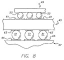
- FIG. 8 is a partial perspective view, partially in section, of an electrical assembly according to one embodiment of the invention, this assembly being adapted for using one or more of the circuitized substrates of the instant invention.
- circuitized substrate as used herein is meant to include substrates having at least one (and preferably more) dielectric layer(s) and at least one (and preferably more) metallurgical conductive layer(s).
- dielectric materials such as fiberglass-reinforced epoxy resins (some referred to as “FR-4” dielectric materials in the art), polytetrafluoroethylene (Teflon), polyimides, polyamides, cyanate resins, photo-imageable materials, and other like materials wherein the conductive layers are each a metal layer (e.g., power, signal and/or ground) comprised of suitable metallurgical materials such as copper, but may include or comprise additional metals (e.g., nickel, aluminum, etc.) or alloys thereof.
- circuitized substrates examples include printed circuit boards (or cards) and chip carriers. It is believed that the teachings of the instant invention are also applicable to what are known as “flex” circuits (which use dielectric materials such as polyimide) and those which use ceramic or other non-polymer type dielectric layers, one example of the latter being what are referred to as multi-layered ceramic (MLC) modules adapted for having one or more semiconductor chips mounted thereon.
- flex circuits which use dielectric materials such as polyimide
- ceramic or other non-polymer type dielectric layers one example of the latter being what are referred to as multi-layered ceramic (MLC) modules adapted for having one or more semiconductor chips mounted thereon.
- MLC multi-layered ceramic
- electrical assembly at least one circuitized substrate as defined herein in combination with at least one electrical component electrically coupled thereto and forming part of the assembly.
- electrical components include chip carriers which include a semiconductor chip as the electrical component, the chip usually positioned on the substrate and coupled to wiring (e.g., pads) on the substrate's outer surface or to internal conductors using one or more thru-holes.
- wiring e.g., pads
- PCB printed circuit board
- the most well known such assembly is the conventional printed circuit board (PCB) typically having several such external electrical components thereon (including possibly one or more chip carriers) and coupled to the internal circuitry of the PCB and/or each other.
- electrical component components such as semiconductor chips and the like which are adapted for being positioned on the external conductive surfaces of such substrates and electrically coupled to the substrate for passing signals from the component into the substrate whereupon such signals may be passed on to other components, including those mounted also on the substrate, as well as other components such as those of a larger electrical system which the substrate forms part of.
- information handling system shall mean any instrumentality or aggregate of instrumentalities primarily designed to compute, classify, process, transmit, receive, retrieve, originate, switch, store, display, manifest, measure, detect, record, reproduce, handle or utilize any form of information, intelligence or data for business, scientific, control or other purposes. Examples include personal computers and larger processors such as servers, mainframes, etc. Such systems typically include one or more PCBs, chip carriers, etc. as integral parts thereof.
- a PCB typically used includes a plurality of various components such as chip carriers, capacitors, resistors, modules, etc. mounted thereon.
- One such PCB can be referred to as a “motherboard” while various other boards (or cards) may be mounted thereon using suitable electrical connectors.
- micro-particles particles having an average size of from about one micron (1000 nanometers) to about fifty microns (50000 nanometers).
- nano-particles as used herein is meant particles with an average size of from about 0.01 micron (ten nanometers) to about one micron (1000 nanometers).
- screen printing is meant to include both screen and stencil printing processes as conventionally used today. These involve the use of a screen or stencil through which a desired material, e.g., inks, conductive compositions, etc., are deposited, e.g., using a squeegee.
- a desired material e.g., inks, conductive compositions, etc.
- blind vias which are openings typically from one surface of a substrate to a predetermined distance therein
- internal vias which are vias or openings located internally of the substrate and are typically formed within one or more internal layers prior to lamination thereof to other layers to form the ultimate structure
- plated through holes also known as PTHS
- a layer 11 of dielectric material is provided.
- the dielectric material for layer 11 may be selected from those listed above, and in one example, may be the aforementioned fiberglass-reinforced epoxy resin (“FR4”) material.
- Atop layer 11 is at least one electrical conductor 13 , preferably of copper or copper alloy.
- conductor 13 is formed from a larger sheet of material bonded (e.g., laminated in solid sheet form using conventional PCB processing) to layer 11 and then subjected to known photolithographic processing used in the PCB industry, to finally define the conductor's configuration. Briefly, in such a process, a photo-resist is applied, patterned and developed (removed in selected locations).
- conductor 13 includes an opening 15 formed (preferably by said etching) therein, but may be of any other acceptable configuration, including more openings, as well as adjacent signal lines, pads, etc.
- conductor 13 may be formed using conventional sputtering operations in which a seed layer is typically provided following which at least one conductive layer is sputtered there-over.
- layer 11 may possess a thickness of from about one mil to about twenty mils (a mil being one-thousandths of an inch) while conductor 13 may include a thickness of from about 0.2 mils to about 2.5 mils.
- conductor 13 is to form part of a circuit for the invention. More particularly, the conductor, with opening 15 therein, may be described as an “anti-pad” meaning that a signal conducting member (e.g., a plated thru-hole, as defined in greater detail below) will pass through the opening and not be in direct electrical contact with the conductor.
- a signal conducting member e.g., a plated thru-hole, as defined in greater detail below
- the next step, prior to which a second dielectric layer 17 ( FIG. 2 ) is to be secured atop conductor 13 is an optional step and involves treating the upper surface of conductor 13 to enhance the adhesion of the dielectric layer 17 to the conductor's surface.
- an oxide (or oxidation) alternative process involves exposing the conductor to what is referred to as a “BondFilm” solution currently available on the marketplace under this name from Atotech Deutschland GmbH, an international company having a U.S.A. business address at 1750 Overview Drive, Rock Hill, S.C.
- BondFilm solution is comprised primarily of three components: (1) sulfuric acid; (2) hydrogen peroxide; and (3) copper, as well as additional Atotech GmbH proprietary constituents. As stated, this process is also referred to as an oxide alternative process, meaning that it does not result in the formation of oxide layers on the treated material.
- the RMS roughness (a standard measurement means) value for the upper surface of conductor 13 after subjecting it to the BondFilm “process” may be about 0.6 microns with a peak of about 1.2 to about 2.2 microns.
- the BondFilm process involves immersing the conductor in the solution for a period of from about 5 to about 120 seconds at a solution temperature of about 20 to 35 degrees Celsius (C).
- this thin organic coating is benzotriazole and possesses a thickness of from about 50 Angstroms to about 500 Angstroms. This thin coating remains on the external surfaces of the conductor during subsequent processing. Because it is so thin, it is not shown in the drawings.
- Other examples of alternative oxide processes which can be utilized with the invention are known in the industry and further description is not deemed necessary.
- Second dielectric layer 17 is now applied, preferably as a solid layer and using a conventional lamination process known in PCB manufacturing.
- Layer 17 is preferably a photo-imageable material, several examples of which are known in the art.
- One example is an ASMDF (Advanced Soldermask Dry Film).
- This composition may include a solids content of from about 85 to about 90%, such solids comprising about 27% PKHC (a phenoxy resin), 41% of Epirez 5183 (a tetrabromobisphenol A), 23% of Epirez SU-8 (an octafunctional epoxy bisphenol A formaldehyde novolac resin), 54% UVE 1014 photo-initiator; 0.07% ethylviolet dye; 0.03% FC 430 (a fluorinated polyether nonionic surfactant from 3M Company), and about 4% Aerosil 380 (an amorphous silicon dioxide from the aforementioned Degussa Corporation) to provide the solid content.
- PKHC a phenoxy resin
- Epirez 5183 a tetrabromobisphenol A
- Epirez SU-8 an octafunctional epoxy bisphenol A formaldehyde novolac resin
- UVE 1014 photo-initiator 0.07% ethylviolet dye
- a solvent is present from about 11 to about 13.5% of the total photo-imageable dielectric composition.
- This composition is known in the art and further description is not deemed necessary.
- several photo-imageable materials may be used, and the invention is not limited to the above.
- the dielectric layer taught herein may be typically about 2 mils to about 4 mils thick, but also thicker or thinner if desired.
- After bonding to the upper surfaces of conductor 13 it is photo-imaged (or photo-patterned), and developed to reveal the desired circuit pattern, in this case at least one opening 19 ( FIG. 3 ) of the same diameter as opening 15 lying immediately there-under. Opening 19 may actually be slightly larger than opening 15 for thin (around 0.2 mils) conductors ( 13 ).
- the dielectric material which is to form layer 17 may be curtain-coated or screen-applied, or it may be supplied as dry film.
- Final cure of the photo-imageable material provides a toughened base of dielectric on which desired electrical circuitry (e.g., signal lines or pads) may be formed. As defined below, it is not necessary to form such circuitry at this time but is more preferable to add yet a third dielectric layer (defined below) prior to such additional circuitry.
- layer 17 may be two mils thick.
- a quantity of resistor material 21 is deposited within aligned openings 15 and 19 , preferably using screen printing (which, per the definition provided above, may include stencil printing as well as conventional screen printing).
- this material comprises a polymer resin (e.g., a cycloaliphatic epoxy resin) and a quantity of metal powder material which may be comprised of one or more metals, each having particles of nano-particle and/or micro-particle size therein.
- resistor material 21 may include only silver particles in the resin mix, while in the second Example, only copper powder may be used in the resin.
- the invention is able to provide resistors with resistance readings from about 120 milliohms (m ⁇ ) to about 120 mega ohms (M ⁇ ), the typical range of resistances for resistors used in PCB and chip carrier applications. It is understood that the invention is capable of providing resistors with resistance readings outside the above range, and the invention is not limited to such a range. It is also understood that the invention is not limited to using only copper and silver as the metals, as others are also possible. In the following Examples, the metal powder(s) used each had particles of from about 0.07 microns to about five microns in size. Here again, the invention is not limited to such sizes and areas.
- the metal component in the resistor composition 21 is, understandably, to establish the resistance of the formed circuit line including the resistor material as part thereof. It also assures improved electrical characteristics of the resistor (e.g. reduced dielectric loss, improved temperature and frequency stability, etc.). Still another purpose of the metal component is to establish the coefficient of thermal expansion (CTE) of the final mixture such that the mixture's CTE more closely approximates the CTE of the final (laminated) substrate and the conductors to which it is joined.
- CTE coefficient of thermal expansion
- the addition of the metal component to the mixture is, therefore, a very important feature of this invention. An important advantage of such closer CTE values is reduced stress within the resulting laminated substrate during substrate operation.
- the resistor material when positioned as shown and thus part of an internal circuit for a circuitized substrate, serves to substantially reduce the capacitance between a pair of electrical conductors (conductor 13 being one of these) and increase the resistance in a formed electrical connection between both electrical conductors. Further explanation is provided below.
- the metal powders used herein are not fired, and, equally significant, are of such a small size so as to enable effective formation of resistive structures (including when used in openings in the dielectric as shown in FIG. 4 ) of such small scale that high density circuit patterns, including those with thru-holes of the type defined above, may be formed.
- Such thru-holes may be of extremely small diameter (in one example, as small as one to two mils) to thereby assure such miniaturized, high density circuit patterns. As indicated, such miniaturization is deemed extremely important with respect to the designs of many present day circuitized substrates.
- resistor material 21 In accomplishing printing of this resistor material 21 , a screen or stencil (not shown) is positioned over layer 17 and the material is forced there-though, e.g., using a squeegee or blade. Material 21 substantially fills openings 15 and 19 and thus physically contacts the respective ends of conductor 13 .
- resistor material 21 may be deposited in paste-like form.
- material 21 it is also possible to apply material 21 as a liquid, dispensing it through a suitable nozzle (not shown) to fill openings 15 and 19 .
- a suitable nozzle not shown
- Use of ink jet printing apparatus having nozzles associated therewith may be used for this.
- resistor material 21 is now “B-staged” (heated in an appropriate oven such as a conventional convection oven) to raise it to a more hardened state than when dispensed.
- material 21 may be heated to a temperature of about 190 degrees Celsius for a period of about two hours.
- the resulting metal particles of resistor material 21 so formed may thus include an oxide coating thereon or may include a coating of the polymer resin material which forms part of the composition as defined. As such, these particles do not form a single continuous conductive path through the resistor material 21 .
- both openings 15 and 19 possessed an internal diameter of about sixteen mils and a total quantity of about 0.09 milligrams of the resistor material 21 was deposited therein.
- material 21 may include a polymer resin as defined herein and a mixture of at least one metal component as defined above and at least one high surface area ceramic component, the nano-particles of the high surface area ceramic component having a particle size substantially within the range of from about 0.01 microns to about 10 microns and a surface area within the range of from about 1 to about 1500 square meters per gram.
- Another resistor material adapted for use herein is a material which includes a polymer resin as defined and a mixture of at least one metal coated ceramic component, the particles of the metal coated ceramic component having a particle size substantially within the range of from about 0.01 microns to about 10 microns.
- the ceramic component is coated with the metal component, to give a mixture including particles of a combined structure of both components.
- the resistor material may include a polymer resin of the type defined herein and at least one oxide coated metal component as defined above, the particles of the oxide coated metal component preferably having a particle size substantially within the range of from about 0.01 microns to about 10 microns.
- Another acceptable resistor material for use herein includes a polymer resin as defined herein and a mixture of at least one metal component and at least one transparent oxide component.
- the particles of the transparent oxide component preferably include a particle size substantially within the range of from about 0.01 microns to about 10 microns, and a surface area within the range of from about 1 to about 100 square meters per gram.
- a resistor material having the unique properties defined herein may include a polymer resin as defined herein and a mixture of at least one metal component and at least one doped manganite component.
- the nano-particles of the doped manganite component preferably have a particle size substantially within the range of from about 0.01 microns to about 10 microns and a surface area within the range of from about 1 to about 100 square meters per gram.
- the mixture may further include a carbon nanotube component.
- these may be in the form of polymer thick film resistors or epoxy-metal (gold, copper, copper-tin) coated polymer sphere based resistors. Sputtering may also be used to deposit the resistor material, using a physical mask.
- Some typical metal alloys for such sputtered resistors include NiP (nickel phosphorous), NiCr (nickel chromium), NiCrAlSi (nickel chromium, aluminum, silicon) and TaN (tantalum nitride). Sputtered and printed resistors may also be used in combination, e.g., where a portion of resistor material is sputtered atop an already printed portion of resistor material.
- a third dielectric layer 23 is positioned over layer 17 and the now partly cured resistor material 21 , said material cured enough to fully support such a layer 23 thereon.
- Layer 23 may be of any of the above dielectric materials, including photo-imageable material as is layer 17 .
- layer 27 is of the conventional “FR4” reinforced resin material and is applied using conventional PCB lamination processing. During such lamination, the temperature of the process also serves to finally (fully) cure the resistor material 21 . In one example, this temperature range may be from about 180 degrees C. to about 380 degrees C. Lamination pressures within the range of 200 pounds per square inch (p.s.i.) to 2500 p.s.i. may be successfully utilized as part of such lamination.
- material 21 may be fully cured prior to layer 23 positioning, e.g., heated to a higher temperature than used to raise it to the “B-stage” described above.
- the invention is thus able to accommodate both possibilities, adding to the versatility of the process defined herein.
- layer 23 is four mils thick.
- layer 23 will actually serve as the second dielectric layer.
- layer 17 may be referred to as an interim dielectric layer, meaning that it is between the initial dielectric layer 11 and the dielectric layer 23 which functions to cover the resistor material.
- Conductors 29 form a circuit pattern on layer 23 which may or may not for part of the circuitry associated with the formed resistor as defined herein. This circuit pattern is shown here to illustrate the possibility of adding such circuitry at this point in the process, if desired.
- the circuitry is formed from a copper foil laminated to layer 23 and then subjected to conventional photolithographic processing as was used above. Other approaches are of course possible, including sputtering, and further description is not deemed needed here.
- each conductor had a thickness of about 1.5 mils and was formed of copper or copper alloy. For ease of description, these conductors may also be referred to herein as “third” conductors.
- layer 30 is formed over conductors 29 and on the upper surface of layer 23 .
- Layer 30 is preferably the aforementioned “FR4” material but maybe of any of the dielectric materials cited above, including a photo-imageable material.
- Layer 30 if of the “FR4” material, is deposited in a single layer form and bonded in place using conventional lamination processing. In one example, pressures within the range of 200 pounds per square inch (PSI.) to 2500 p.s.i. and temperatures of from about 180 degrees C. to about 380 degrees C. may be used as part of such lamination processing. Notably, these elevated temperatures do not adversely affect the resistor material 21 . In one example, layer 30 may be four mils thick.
- Conductor 31 is preferably formed using conventional photolithographic processing following deposition of a single sheet of the conductor (preferably copper or copper alloy) onto layer 30 . It is understood of course that many such conductors 31 may be formed, as well as other conductive elements such a signal lines or pads, all to form part of a single layer of circuitry at this location in the invention. Conductor 31 may be 1.5 mils thick and, as shown, is located over resistor material 21 .
- dielectric layer 17 is what might be referred to also as an interim dielectric layer, being formed following formation of conductor 13 (including with its opening 15 therein) and prior to positioning of dielectric layer 23 .
- opening 35 may be formed using mechanical or laser drilling, one of these being the use of an Ng-YAG laser.
- opening 35 may possess a diameter of eight mils and extends through the entire thickness of the FIG. 6 (and now FIG. 7 ) structure.
- This opening passes through the top conductor 31 and through the opening 15 within the initial conductor 13 , thereby not directly contacting the internal walls of conductor 13 .
- this opening passes directly through (and thus engages) the resistor material 21 .
- the internal walls of the opening are metallized, preferably using a conventional electroplating operation used in plating PCB thru-holes.
- a preferred electroplating process used in the formation of known PTHs may be used here, in which a first thin layer of palladium seed is applied, followed by a thin layer of electro-less copper, and finally, a thicker layer of electrolytic copper, resulting in the formation of a thin layer 37 (e.g., about 0.5 mils thick) on the openings internal walls.
- a thin layer 37 e.g., about 0.5 mils thick
- This conductive material thus provides an electrical path from the top conductor 31 down through the substrate to the resistor material 21 , and thus the other conductor 13 .
- the opening and plated conductive material thereby forms a thru-hole 41 , which, in the FIG. 7 embodiment, extends through the full thickness of the structure.
- This circuit path for the substrate thus includes a resistor as part thereof.
- the invention as defined herein may result in several such circuits being formed, and the invention is not limited to a single circuit and a single resistor as shown. In fact, the invention may provide more than one resistor per circuit, if desired.
- circuit path (and structure) of FIG. 7 there are distinctive advantages of the circuit path (and structure) of FIG. 7 , especially when there is a concern for performance degradation as a result of discontinuities (mentioned above) in the signal path through the circuit, as is always the concern for circuit designers of high density circuit patterns as taught herein.
- the circuit of FIG. 7 there is the advantage of utilizing a material (resistor material 21 ) which possesses less capacitance than the dielectric material (layer 17 ) it replaces, thereby decreasing the capacitance in the circuit between conductors 13 and 31 .
- the resulting capacitance (indicated by dimension “C” in FIG. 7 ) measured as low as from about 0.05 picofarads to about 0.22 picofarads.
- This design also reduces the signal energy that will reflect from the open end of the thru-hole 41 (that end which extends through dielectric layer 11 ).
- the resistance value is very carefully selected so as to draw very little energy from the signal passing through the circuit.
- a 50-ohm impedance signal line (path) is not affected significantly by 100,000 ohms in parallel, but the unwanted energy which travels down the thru-hole 41 is strongly affected by the additional 100,000 ohms because the thru-hole is open at the lower end. Therefore, much of the signal energy in this “stub” (end portion) will pass through the resistor material instead of “bouncing off” the open end.
- FIG. 8 represents examples of the structures defined herein-above, the assembly referenced by the numeral 45 being a chip carrier, while the assembly represented by the numeral 47 is a PCB. Each is capable of including one or more internal resistors of the type defined above as part thereof. Both such PCB and chip carrier assemblies are produced and sold by the Assignee of the invention.
- the chip carrier 45 is mounted on and electrically coupled to PCB 47 using a plurality of solder balls 51 (preferably of conventional tin-lead composition), the chip carrier 45 in turn having a semiconductor chip 49 positioned thereon and electrically coupled to the carrier using the second plurality of solder balls 53 (also preferably of conventional tin-lead composition).
- FIG. 8 there are two electrical assemblies shown in FIG. 8 , one being the carrier-chip assembly and the other the PCB-carrier assembly (which inherently includes chip 49 ).
- the structure in FIG. 8 may also include a heat sink (not shown) thermally coupled to chip 49 , e.g., using a conductive paste, and positioned on the upper surface of carrier 45 by appropriate standoffs, as is known in the art.
- a heat sink thermally coupled to chip 49 , e.g., using a conductive paste
- an encapsulant material (not shown) to substantially encase the chip and also to possibly eliminate the need for the heat sink if such an encapsulant material is used.
- Encapsulant material is also possible about the lower pluralities of solder balls 51 and 53 .
- solder balls 53 interconnect contact sites (not shown) on the chip's underside to corresponding pads 61 on carrier 45 .
- solder balls 51 interconnect pads 63 on the carrier's undersurface with pads 65 on the upper surface of PCB 47 .
- pads are typically of copper or copper alloy and are known in the PCB art.
- one or more of the upper pads 61 may be coupled to corresponding ones of the lower pads 63 to form individual circuit paths there-between.
- One or more of these circuit paths may include one or more of the resistors as taught herein.
- circuitized substrates of the type formed herein may be utilized in what are referred to in the art as “information handling systems” (defined above).
- systems include personal computers, a mainframe computers and computer servers.
- Other types of information handling systems known in the art of this type may also utilize the teachings of this invention.
- the circuitized substrate or substrates as formed in accordance with the teachings herein, each including one or more internal resistors as taught above, may be utilized in the system, e.g., as a “mother board” or as one or more individual PCBs.
- Examples 1-5 represent micro-particle based resistors and Examples 6 and 7 represent nano-particle based resistors.
- cycloaliphatic epoxy resin e.g., one sold under product designation “ERL-4211” by the Union Carbide Corporation, Danbury, Conn.
- ERL-4211 a cycloaliphatic epoxy resin
- the mixed solution was stirred for approximately ten minutes to assure uniform mixing.
- Fifty gm of silver powder available from Degussa Corporation (having a business location at 379 Interpace Parkway, Parsippany, N.J.) was added to 7.5 gm of the mixed solution and formed into a printable paste.
- the silver powder included particles with an average size of about five microns.
- a layer of this paste material was then printed onto a copper substrate. This layer was then cured at approximately 190 degrees Celsius (C) for about two hours. The resistance of the cured resistors (3 inch long and 0.003 square inch cross section area) measured about 120 milliohms (m ⁇ ).
- Fifty gm of the “ERL-4211” cycloaliphatic epoxy resin was mixed with about fifty gm of hexahydro-4-methylphthalic anhydride and 0.4 gm N,N dimethyl benzylamine. The mixed solution was stirred for about ten minutes to assure uniform mixing.
- Fifty gm of copper powder was added to 7.5 gm of the mixed solution and formed into a printable paste. The copper powder included particles with an average size of about four microns.
- a layer of this paste material was printed onto a copper substrate. This layer was then cured at approximately 190° C. for about two hours. The resistance of the cured resistors (3 inch long and 0.003 square inch cross section area) measured about 120 Mega ohms (M ⁇ ).
- Fifty gm of the “ERL-4211” cycloaliphatic epoxy resin was mixed with about fifty gm of hexahydro-4-methylphthalic anhydride and 0.4 gm N,N dimethyl benzylamine. The mixed solution was stirred for about ten minutes to assure uniform mixing. Thirty-eight gm of copper and twelve gm of silver powder was added to 7.5 gm of the mixed solution and formed into a printable paste. The average particle sizes for the copper and silver powders ranged from about four to about five microns in diameter. A layer of this paste material was printed onto a copper substrate. This layer was then cured at approximately 190° C. for about two hours. The resistance of the cured resistors (3 inch long and 0.003 square inch cross section area) measured about 70 Mega ohms (M ⁇ ).
- Fifty gm of the “ERL-4211” cycloaliphatic epoxy resin was mixed with about fifty gm of hexahydro-4-methylphthalic anhydride and 0.4 gm N,N dimethyl benzylamine. The mixed solution was stirred for approximately ten minutes to assure uniform mixing.
- Five gm of copper and forty-five gm of silver powder was added to 7.5 gm of the mixed solution and formed into a printable paste. The average particle sizes for the copper and silver powders ranged from about four to about five microns in diameter.
- a layer of this paste material was printed onto a copper substrate. This layer was then cured at approximately 190° C. for about two hours.
- the resistance of the cured resistors (3 inch long and 0.003 square inch cross section area) measured about 400 milliohms (m ⁇ ).
- Fifty gm of the “ERL-4211” cycloaliphatic epoxy resin was mixed with about fifty gm of hexahydro-4-methylphthalic anhydride and 0.4 gm N,N dimethyl benzylamine. The mixed solution was stirred for about ten minutes to assure uniform mixing. Twenty gm of copper and thirty gm of silver powder was added to 7.5 gm of the mixed solution and formed into a printable paste. The average particle sizes for the copper and silver powders ranged from about four to about five microns in diameter. A layer of this paste material was printed onto a copper substrate. This layer was then cured at approximately 190° C. for about two hours. The resistance of the cured resistors (3 inch long and 0.003 square inch cross section area) measured about 25 ohm ( ⁇ ).
- Fifty gm of the “ERL-4211” cycloaliphatic epoxy resin was mixed with about fifty gm of hexahydro-4-methylphthalic anhydride and 0.4 gm N,N dimethyl benzylamine. The mixed solution was stirred for about ten minutes to assure uniform mixing.
- Four gm of fluorinated graphite available from Alfa Aesear, Ward Hill, Mass. and 5.4 gm silver nano-powders available from Cima NanoTech, Inc., North Industrial Park, Caesarea, Israel, having a D90 particle size of 0.07 micron was added to 7.5 gm of the mixed solution and formed into a printable paste. A layer of this paste material was printed onto a copper substrate. This layer was then cured at approximately 200 degrees C. for about two hours. The resistance of the cured resistors (3 inch long and 0.003 square inch cross section area) measured about 90 ohm ( ⁇ ).
- Fifty gm of the “ERL-4211” cycloaliphatic epoxy resin was mixed with about fifty gm of hexahydro-4-methylphthalic anhydride and 0.4 gm N,N dimethyl benzylamine. The mixed solution was stirred for about ten minutes to assure uniform mixing.
- Four gm of fluorinated graphite available from Alfa Aesear and four gm silver nano-powders available from Cima NanoTech, Inc., having a D90 particle size of 0.07 micron was added to 7.5 gm of the mixed solution and formed into a printable paste. A layer of this paste material was printed onto a copper substrate. This layer was then cured at approximately 200 degrees C. for about two hours. The resistance of the cured resistors (3 inch long and 0.003 square inch cross section area) measured about 20 Mega ohms (M ⁇ ).
- circuitized substrate having one or more internal resistors as part thereof, which substrate can be formed using many conventional PCB processes to thereby reduce costs associated with production thereof.
- the substrates produced herein are readily adaptable for use in electrical assemblies in which one or more electrical components such as semiconductor chips may be positioned thereon and coupled thereto.
- resistor materials which can be positioned between two adjacent conductors as part of such a circuit line to form circuitry for these substrates.
- the invention affords the opportunity to vary the resistances between conductors by varying the resistor material composition, as represented by the foregoing Examples. Such latitude greatly assists the circuit designer in meeting varying operational requirements.
- the invention as defined herein is capable of transmitting both regular and high speed (frequency) signals, the latter at a rate of from about one Gigabits/sec to about ten Gigabits/second, while substantially preventing impedance disruption. It is also capable of being produced using many conventional PCB processes so as to assure reduced cost and facilitate ease of manufacture. Of perhaps greater significance, the invention is able to assure circuit pattern miniaturization as is deemed extremely important with regards to many of today's design requirements.
Landscapes
- Engineering & Computer Science (AREA)
- Microelectronics & Electronic Packaging (AREA)
- Chemical & Material Sciences (AREA)
- Dispersion Chemistry (AREA)
- Production Of Multi-Layered Print Wiring Board (AREA)
- Parts Printed On Printed Circuit Boards (AREA)
Abstract
Description
| TABLE |
| Resistance Change with Silver/Copper Ratio. |
| Metal | Polymer | Resistor size | Resistance |
| 50 gm silver | 7.5 gm | 3 inch long and 0.003 square | 120 mΩ |
| inch |
|||
| 45 gm silver + 5 gm | 7.5 gm | 3 inch long and 0.003 square | 400 mΩ |
| Cu | inch |
||
| 30 gm silver + | 7.5 gm | 3 inch long and 0.003 square | 25 Ω |
| 20 gm Cu | inch cross section area | ||
| 12 gm silver + | 7.5 gm | 3 inch long and 0.003 square | 70 MΩ |
| 38 gm Cu | inch cross section area | ||
| 50 gm Cu | 7.5 gm | 3 inch long and 0.003 square | 120 MΩ |
| inch cross section area | |||
Claims (10)
Priority Applications (4)
| Application Number | Priority Date | Filing Date | Title |
|---|---|---|---|
| US11/806,685 US7687724B2 (en) | 2005-01-10 | 2007-06-04 | Circuitized substrate with internal resistor, method of making said circuitized substrate, and electrical assembly utilizing said circuitized substrate |
| TW97118394A TW200908828A (en) | 2007-06-04 | 2008-05-19 | Circuitized substrate with internal resistor, method of making said circuitized substrate, and electrical assembly utilizing said circuitized substrate |
| JP2008145499A JP2008300846A (en) | 2007-06-04 | 2008-06-03 | Circuit board which has internal register, and electric assembly using this circuit board |
| US12/589,239 US9420689B2 (en) | 2005-01-10 | 2009-10-20 | Method of making a circuitized substrate |
Applications Claiming Priority (3)
| Application Number | Priority Date | Filing Date | Title |
|---|---|---|---|
| US11/031,074 US7025607B1 (en) | 2005-01-10 | 2005-01-10 | Capacitor material with metal component for use in circuitized substrates, circuitized substrate utilizing same, method of making said circuitized substrate, and information handling system utilizing said circuitized substrate |
| US11/172,786 US7235745B2 (en) | 2005-01-10 | 2005-07-05 | Resistor material with metal component for use in circuitized substrates, circuitized substrate utilizing same, method of making said ciruitized substrate, and information handling system utilizing said ciruitized substrate |
| US11/806,685 US7687724B2 (en) | 2005-01-10 | 2007-06-04 | Circuitized substrate with internal resistor, method of making said circuitized substrate, and electrical assembly utilizing said circuitized substrate |
Related Parent Applications (2)
| Application Number | Title | Priority Date | Filing Date |
|---|---|---|---|
| US11/031,074 Continuation-In-Part US7025607B1 (en) | 2005-01-10 | 2005-01-10 | Capacitor material with metal component for use in circuitized substrates, circuitized substrate utilizing same, method of making said circuitized substrate, and information handling system utilizing said circuitized substrate |
| US11/172,786 Continuation-In-Part US7235745B2 (en) | 2005-01-10 | 2005-07-05 | Resistor material with metal component for use in circuitized substrates, circuitized substrate utilizing same, method of making said ciruitized substrate, and information handling system utilizing said ciruitized substrate |
Related Child Applications (1)
| Application Number | Title | Priority Date | Filing Date |
|---|---|---|---|
| US12/589,239 Division US9420689B2 (en) | 2005-01-10 | 2009-10-20 | Method of making a circuitized substrate |
Publications (2)
| Publication Number | Publication Date |
|---|---|
| US20080087459A1 US20080087459A1 (en) | 2008-04-17 |
| US7687724B2 true US7687724B2 (en) | 2010-03-30 |
Family
ID=40193972
Family Applications (2)
| Application Number | Title | Priority Date | Filing Date |
|---|---|---|---|
| US11/806,685 Expired - Fee Related US7687724B2 (en) | 2005-01-10 | 2007-06-04 | Circuitized substrate with internal resistor, method of making said circuitized substrate, and electrical assembly utilizing said circuitized substrate |
| US12/589,239 Expired - Fee Related US9420689B2 (en) | 2005-01-10 | 2009-10-20 | Method of making a circuitized substrate |
Family Applications After (1)
| Application Number | Title | Priority Date | Filing Date |
|---|---|---|---|
| US12/589,239 Expired - Fee Related US9420689B2 (en) | 2005-01-10 | 2009-10-20 | Method of making a circuitized substrate |
Country Status (1)
| Country | Link |
|---|---|
| US (2) | US7687724B2 (en) |
Cited By (7)
| Publication number | Priority date | Publication date | Assignee | Title |
|---|---|---|---|---|
| US20080296254A1 (en) * | 2003-07-02 | 2008-12-04 | Tessera Interconnect Materials, Inc. | Multilayer wiring board for an electronic device |
| US20090250249A1 (en) * | 2008-04-04 | 2009-10-08 | Racz Livia M | Interposers, electronic modules, and methods for forming the same |
| US20110209909A1 (en) * | 2011-05-05 | 2011-09-01 | Mixzon Incorporated | Noise dampening energy efficient circuit board and method for constructing and using same |
| US8535984B2 (en) | 2008-04-04 | 2013-09-17 | The Charles Stark Draper Laboratory, Inc. | Electronic modules and methods for forming the same |
| CN105517343A (en) * | 2016-01-25 | 2016-04-20 | 东莞联桥电子有限公司 | Method for resistor integration on microwave printed circuit board |
| US9768555B2 (en) * | 2015-06-23 | 2017-09-19 | Dell Products L.P. | Systems and methods for frequency shifting resonance of connector stubs |
| US10269841B1 (en) * | 2017-09-29 | 2019-04-23 | Phoenix & Corporation | Sensor package and method of manufacturing the same |
Families Citing this family (22)
| Publication number | Priority date | Publication date | Assignee | Title |
|---|---|---|---|---|
| US7687724B2 (en) * | 2005-01-10 | 2010-03-30 | Endicott Interconnect Technologies, Inc. | Circuitized substrate with internal resistor, method of making said circuitized substrate, and electrical assembly utilizing said circuitized substrate |
| KR101551501B1 (en) * | 2007-03-10 | 2015-09-08 | 산미나 코포레이션 | embedded capacitive stack |
| KR100891531B1 (en) * | 2007-09-10 | 2009-04-03 | 주식회사 하이닉스반도체 | Pattern misalignment detection device |
| US8557700B2 (en) * | 2008-05-09 | 2013-10-15 | Invensas Corporation | Method for manufacturing a chip-size double side connection package |
| US7791897B2 (en) * | 2008-09-09 | 2010-09-07 | Endicott Interconnect Technologies, Inc. | Multi-layer embedded capacitance and resistance substrate core |
| KR20100048610A (en) | 2008-10-31 | 2010-05-11 | 삼성전자주식회사 | Semiconductor fackage and forming method of the same |
| US8026111B2 (en) * | 2009-02-24 | 2011-09-27 | Oracle America, Inc. | Dielectric enhancements to chip-to-chip capacitive proximity communication |
| US20110017498A1 (en) * | 2009-07-27 | 2011-01-27 | Endicott Interconnect Technologies, Inc. | Photosensitive dielectric film |
| US9351408B2 (en) * | 2010-04-22 | 2016-05-24 | I3 Electronics, Inc. | Coreless layer buildup structure with LGA and joining layer |
| US20130070437A1 (en) * | 2011-09-20 | 2013-03-21 | Invensas Corp. | Hybrid interposer |
| US20140000099A1 (en) * | 2012-06-29 | 2014-01-02 | Noah Austin Spivak | Methods for building resistive elements into printed circuit boards |
| US8847349B2 (en) * | 2012-12-21 | 2014-09-30 | Texas Instruments Incorporated | Integrated circuit package with printed circuit layer |
| KR20150074649A (en) * | 2013-12-24 | 2015-07-02 | 삼성전기주식회사 | Semiconductor package and manufacturing method thereof |
| CN104752329B (en) * | 2013-12-30 | 2017-12-01 | 中芯国际集成电路制造(上海)有限公司 | The forming method of interconnection structure |
| US9955568B2 (en) * | 2014-01-24 | 2018-04-24 | Dell Products, Lp | Structure to dampen barrel resonance of unused portion of printed circuit board via |
| TWI589195B (en) * | 2014-05-09 | 2017-06-21 | Sensitive and perforated circuit board and multilayer circuit board | |
| FR3036918B1 (en) * | 2015-05-29 | 2018-08-10 | Thales | ELECTRONIC CARD AND METHOD OF MANUFACTURING THE SAME |
| CN106163083B (en) * | 2016-06-30 | 2017-08-15 | 广州番禺运升电路版有限公司 | A kind of Printed circuit board and manufacturing methods |
| US10181447B2 (en) | 2017-04-21 | 2019-01-15 | Invensas Corporation | 3D-interconnect |
| CN211045436U (en) * | 2019-07-07 | 2020-07-17 | 深南电路股份有限公司 | circuit board |
| CN111053298B (en) * | 2019-12-20 | 2022-03-15 | 深圳麦克韦尔科技有限公司 | Flexible heating element and manufacturing method thereof, flexible heating assembly and aerosol generator |
| US12040284B2 (en) | 2021-11-12 | 2024-07-16 | Invensas Llc | 3D-interconnect with electromagnetic interference (“EMI”) shield and/or antenna |
Citations (29)
| Publication number | Priority date | Publication date | Assignee | Title |
|---|---|---|---|---|
| US5016085A (en) | 1988-03-04 | 1991-05-14 | Hughes Aircraft Company | Hermetic package for integrated circuit chips |
| US5079069A (en) | 1989-08-23 | 1992-01-07 | Zycon Corporation | Capacitor laminate for use in capacitive printed circuit boards and methods of manufacture |
| US5099309A (en) | 1990-04-30 | 1992-03-24 | International Business Machines Corporation | Three-dimensional memory card structure with internal direct chip attachment |
| US5162977A (en) | 1991-08-27 | 1992-11-10 | Storage Technology Corporation | Printed circuit board having an integrated decoupling capacitive element |
| US5280192A (en) | 1990-04-30 | 1994-01-18 | International Business Machines Corporation | Three-dimensional memory card structure with internal direct chip attachment |
| US5426263A (en) | 1993-12-23 | 1995-06-20 | Motorola, Inc. | Electronic assembly having a double-sided leadless component |
| US5831833A (en) | 1995-07-17 | 1998-11-03 | Nec Corporation | Bear chip mounting printed circuit board and a method of manufacturing thereof by photoetching |
| US6021050A (en) | 1998-12-02 | 2000-02-01 | Bourns, Inc. | Printed circuit boards with integrated passive components and method for making same |
| US6068782A (en) | 1998-02-11 | 2000-05-30 | Ormet Corporation | Individual embedded capacitors for laminated printed circuit boards |
| US6084306A (en) | 1998-05-29 | 2000-07-04 | Texas Instruments Incorporated | Bridging method of interconnects for integrated circuit packages |
| US6150456A (en) | 1997-09-11 | 2000-11-21 | E. I. Du Pont De Nemours And Company | High dielectric constant flexible polyimide film and process of preparation |
| US6207595B1 (en) | 1998-03-02 | 2001-03-27 | International Business Machines Corporation | Laminate and method of manufacture thereof |
| US6242282B1 (en) | 1999-10-04 | 2001-06-05 | General Electric Company | Circuit chip package and fabrication method |
| US6370012B1 (en) | 2000-08-30 | 2002-04-09 | International Business Machines Corporation | Capacitor laminate for use in printed circuit board and as an interconnector |
| US6396387B1 (en) | 1998-04-29 | 2002-05-28 | Microcoating Technologies, Inc. | Resistors for electronic packaging |
| US6395996B1 (en) | 2000-05-16 | 2002-05-28 | Silicon Integrated Systems Corporation | Multi-layered substrate with a built-in capacitor design |
| US6446317B1 (en) | 2000-03-31 | 2002-09-10 | Intel Corporation | Hybrid capacitor and method of fabrication therefor |
| US6500350B1 (en) | 1998-04-29 | 2002-12-31 | Morton International, Inc. | Formation of thin film resistors |
| US6544651B2 (en) | 2000-05-18 | 2003-04-08 | Georgia Tech Research Corp. | High dielectric constant nano-structure polymer-ceramic composite |
| US20030146418A1 (en) * | 2001-10-25 | 2003-08-07 | Chacko Antony P. | Resistive film |
| US6616794B2 (en) | 1998-05-04 | 2003-09-09 | Tpl, Inc. | Integral capacitance for printed circuit board using dielectric nanopowders |
| US6704207B2 (en) | 2000-05-25 | 2004-03-09 | Hewlett-Packard Development Company, L.P. | Device and method for interstitial components in a printed circuit board |
| US6746508B1 (en) * | 1999-10-22 | 2004-06-08 | Chrysalis Technologies Incorporated | Nanosized intermetallic powders |
| US20040231758A1 (en) * | 1997-02-24 | 2004-11-25 | Hampden-Smith Mark J. | Silver-containing particles, method and apparatus of manufacture, silver-containing devices made therefrom |
| US20050000728A1 (en) | 2003-07-03 | 2005-01-06 | Shinko Electric Industries Co., Ltd. | Wiring board provided with a resistor and process for manufacturing the same |
| US20050051360A1 (en) * | 2003-09-08 | 2005-03-10 | Te-Yeu Su | Polymer thick-film resistive paste, a polymer thick-film resistor and a method and an apparatus for the manufacture thereof |
| US6967138B2 (en) * | 2003-06-19 | 2005-11-22 | Advanced Semiconductor Engineering, Inc. | Process for manufacturing a substrate with embedded capacitor |
| US7025607B1 (en) | 2005-01-10 | 2006-04-11 | Endicott Interconnect Technologies, Inc. | Capacitor material with metal component for use in circuitized substrates, circuitized substrate utilizing same, method of making said circuitized substrate, and information handling system utilizing said circuitized substrate |
| US7342802B2 (en) * | 2003-07-02 | 2008-03-11 | Tessera Interconnect Materials, Inc. | Multilayer wiring board for an electronic device |
Family Cites Families (5)
| Publication number | Priority date | Publication date | Assignee | Title |
|---|---|---|---|---|
| US6542352B1 (en) * | 1997-12-09 | 2003-04-01 | Daniel Devoe | Ceramic chip capacitor of conventional volume and external form having increased capacitance from use of closely spaced interior conductive planes reliably connecting to positionally tolerant exterior pads through multiple redundant vias |
| US7217981B2 (en) * | 2005-01-06 | 2007-05-15 | International Business Machines Corporation | Tunable temperature coefficient of resistance resistors and method of fabricating same |
| US7235745B2 (en) * | 2005-01-10 | 2007-06-26 | Endicott Interconnect Technologies, Inc. | Resistor material with metal component for use in circuitized substrates, circuitized substrate utilizing same, method of making said ciruitized substrate, and information handling system utilizing said ciruitized substrate |
| US7687724B2 (en) * | 2005-01-10 | 2010-03-30 | Endicott Interconnect Technologies, Inc. | Circuitized substrate with internal resistor, method of making said circuitized substrate, and electrical assembly utilizing said circuitized substrate |
| US8240027B2 (en) * | 2008-01-16 | 2012-08-14 | Endicott Interconnect Technologies, Inc. | Method of making circuitized substrates having film resistors as part thereof |
-
2007
- 2007-06-04 US US11/806,685 patent/US7687724B2/en not_active Expired - Fee Related
-
2009
- 2009-10-20 US US12/589,239 patent/US9420689B2/en not_active Expired - Fee Related
Patent Citations (31)
| Publication number | Priority date | Publication date | Assignee | Title |
|---|---|---|---|---|
| US5016085A (en) | 1988-03-04 | 1991-05-14 | Hughes Aircraft Company | Hermetic package for integrated circuit chips |
| US5079069A (en) | 1989-08-23 | 1992-01-07 | Zycon Corporation | Capacitor laminate for use in capacitive printed circuit boards and methods of manufacture |
| US5280192A (en) | 1990-04-30 | 1994-01-18 | International Business Machines Corporation | Three-dimensional memory card structure with internal direct chip attachment |
| US5099309A (en) | 1990-04-30 | 1992-03-24 | International Business Machines Corporation | Three-dimensional memory card structure with internal direct chip attachment |
| US5162977A (en) | 1991-08-27 | 1992-11-10 | Storage Technology Corporation | Printed circuit board having an integrated decoupling capacitive element |
| US5426263A (en) | 1993-12-23 | 1995-06-20 | Motorola, Inc. | Electronic assembly having a double-sided leadless component |
| US5831833A (en) | 1995-07-17 | 1998-11-03 | Nec Corporation | Bear chip mounting printed circuit board and a method of manufacturing thereof by photoetching |
| US20040231758A1 (en) * | 1997-02-24 | 2004-11-25 | Hampden-Smith Mark J. | Silver-containing particles, method and apparatus of manufacture, silver-containing devices made therefrom |
| US6150456A (en) | 1997-09-11 | 2000-11-21 | E. I. Du Pont De Nemours And Company | High dielectric constant flexible polyimide film and process of preparation |
| US6068782A (en) | 1998-02-11 | 2000-05-30 | Ormet Corporation | Individual embedded capacitors for laminated printed circuit boards |
| US6207595B1 (en) | 1998-03-02 | 2001-03-27 | International Business Machines Corporation | Laminate and method of manufacture thereof |
| US6396387B1 (en) | 1998-04-29 | 2002-05-28 | Microcoating Technologies, Inc. | Resistors for electronic packaging |
| US6500350B1 (en) | 1998-04-29 | 2002-12-31 | Morton International, Inc. | Formation of thin film resistors |
| US6616794B2 (en) | 1998-05-04 | 2003-09-09 | Tpl, Inc. | Integral capacitance for printed circuit board using dielectric nanopowders |
| US6084306A (en) | 1998-05-29 | 2000-07-04 | Texas Instruments Incorporated | Bridging method of interconnects for integrated circuit packages |
| US6021050A (en) | 1998-12-02 | 2000-02-01 | Bourns, Inc. | Printed circuit boards with integrated passive components and method for making same |
| US6242282B1 (en) | 1999-10-04 | 2001-06-05 | General Electric Company | Circuit chip package and fabrication method |
| US6746508B1 (en) * | 1999-10-22 | 2004-06-08 | Chrysalis Technologies Incorporated | Nanosized intermetallic powders |
| US6446317B1 (en) | 2000-03-31 | 2002-09-10 | Intel Corporation | Hybrid capacitor and method of fabrication therefor |
| US6395996B1 (en) | 2000-05-16 | 2002-05-28 | Silicon Integrated Systems Corporation | Multi-layered substrate with a built-in capacitor design |
| US6544651B2 (en) | 2000-05-18 | 2003-04-08 | Georgia Tech Research Corp. | High dielectric constant nano-structure polymer-ceramic composite |
| US6704207B2 (en) | 2000-05-25 | 2004-03-09 | Hewlett-Packard Development Company, L.P. | Device and method for interstitial components in a printed circuit board |
| US6524352B2 (en) | 2000-08-30 | 2003-02-25 | International Business Machines Corporation | Method of making a parallel capacitor laminate |
| US6370012B1 (en) | 2000-08-30 | 2002-04-09 | International Business Machines Corporation | Capacitor laminate for use in printed circuit board and as an interconnector |
| US6740701B2 (en) | 2001-10-25 | 2004-05-25 | Cts Corporation | Resistive film |
| US20030146418A1 (en) * | 2001-10-25 | 2003-08-07 | Chacko Antony P. | Resistive film |
| US6967138B2 (en) * | 2003-06-19 | 2005-11-22 | Advanced Semiconductor Engineering, Inc. | Process for manufacturing a substrate with embedded capacitor |
| US7342802B2 (en) * | 2003-07-02 | 2008-03-11 | Tessera Interconnect Materials, Inc. | Multilayer wiring board for an electronic device |
| US20050000728A1 (en) | 2003-07-03 | 2005-01-06 | Shinko Electric Industries Co., Ltd. | Wiring board provided with a resistor and process for manufacturing the same |
| US20050051360A1 (en) * | 2003-09-08 | 2005-03-10 | Te-Yeu Su | Polymer thick-film resistive paste, a polymer thick-film resistor and a method and an apparatus for the manufacture thereof |
| US7025607B1 (en) | 2005-01-10 | 2006-04-11 | Endicott Interconnect Technologies, Inc. | Capacitor material with metal component for use in circuitized substrates, circuitized substrate utilizing same, method of making said circuitized substrate, and information handling system utilizing said circuitized substrate |
Cited By (11)
| Publication number | Priority date | Publication date | Assignee | Title |
|---|---|---|---|---|
| US20080296254A1 (en) * | 2003-07-02 | 2008-12-04 | Tessera Interconnect Materials, Inc. | Multilayer wiring board for an electronic device |
| US9521755B2 (en) | 2003-07-02 | 2016-12-13 | Invensas Corporation | Multilayer wiring board for an electronic device |
| US10104785B2 (en) | 2003-07-02 | 2018-10-16 | Invensas Corporation | Multilayer wiring board for an electronic device |
| US20090250249A1 (en) * | 2008-04-04 | 2009-10-08 | Racz Livia M | Interposers, electronic modules, and methods for forming the same |
| US8273603B2 (en) | 2008-04-04 | 2012-09-25 | The Charles Stark Draper Laboratory, Inc. | Interposers, electronic modules, and methods for forming the same |
| US8535984B2 (en) | 2008-04-04 | 2013-09-17 | The Charles Stark Draper Laboratory, Inc. | Electronic modules and methods for forming the same |
| US20110209909A1 (en) * | 2011-05-05 | 2011-09-01 | Mixzon Incorporated | Noise dampening energy efficient circuit board and method for constructing and using same |
| US8569631B2 (en) * | 2011-05-05 | 2013-10-29 | Tangitek, Llc | Noise dampening energy efficient circuit board and method for constructing and using same |
| US9768555B2 (en) * | 2015-06-23 | 2017-09-19 | Dell Products L.P. | Systems and methods for frequency shifting resonance of connector stubs |
| CN105517343A (en) * | 2016-01-25 | 2016-04-20 | 东莞联桥电子有限公司 | Method for resistor integration on microwave printed circuit board |
| US10269841B1 (en) * | 2017-09-29 | 2019-04-23 | Phoenix & Corporation | Sensor package and method of manufacturing the same |
Also Published As
| Publication number | Publication date |
|---|---|
| US9420689B2 (en) | 2016-08-16 |
| US20080087459A1 (en) | 2008-04-17 |
| US20110039212A1 (en) | 2011-02-17 |
Similar Documents
| Publication | Publication Date | Title |
|---|---|---|
| US7687724B2 (en) | Circuitized substrate with internal resistor, method of making said circuitized substrate, and electrical assembly utilizing said circuitized substrate | |
| US7870664B2 (en) | Method of making circuitized substrate with a resistor | |
| US7025607B1 (en) | Capacitor material with metal component for use in circuitized substrates, circuitized substrate utilizing same, method of making said circuitized substrate, and information handling system utilizing said circuitized substrate | |
| US7541265B2 (en) | Capacitor material for use in circuitized substrates, circuitized substrate utilizing same, method of making said circuitized substrate, and information handling system utilizing said circuitized substrate | |
| US9756724B2 (en) | Method of making a circuitized substrate | |
| US7442879B2 (en) | Circuitized substrate with solder-coated microparticle paste connections, multilayered substrate assembly, electrical assembly and information handling system utilizing same and method of making said substrate | |
| US7384856B2 (en) | Method of making an internal capacitive substrate for use in a circuitized substrate and method of making said circuitized substrate | |
| US8299371B2 (en) | Circuitized substrate with dielectric interposer assembly and method | |
| US7803688B2 (en) | Capacitive substrate and method of making same | |
| US7449381B2 (en) | Method of making a capacitive substrate for use as part of a larger circuitized substrate, method of making said circuitized substrate and method of making an information handling system including said circuitized substrate | |
| US20070177331A1 (en) | Non-flaking capacitor material, capacitive substrate having an internal capacitor therein including said non-flaking capacitor material, and method of making a capacitor member for use in a capacitive substrate | |
| JPH11126978A (en) | Multilayer wiring board | |
| US7429510B2 (en) | Method of making a capacitive substrate using photoimageable dielectric for use as part of a larger circuitized substrate, method of making said circuitized substrate and method of making an information handling system including said circuitized substrate | |
| US20080022520A1 (en) | Method of making multilayered circuitized substrate assembly | |
| US20120228014A1 (en) | Circuitized substrate with internal thin film capacitor and method of making same | |
| US7334323B2 (en) | Method of making mutilayered circuitized substrate assembly having sintered paste connections | |
| JP2008300846A (en) | Circuit board which has internal register, and electric assembly using this circuit board | |
| JP2001244367A (en) | Wiring board with built-in electric element | |
| JP2001102754A (en) | Multilayer wiring board | |
| HK1127839A (en) | Circuitized substrate with conductive paste |
Legal Events
| Date | Code | Title | Description |
|---|---|---|---|
| AS | Assignment |
Owner name: ENDICOTT INTERCONNECT TECHNOLOGIES, INC., NEW YORK Free format text: ASSIGNMENT OF ASSIGNORS INTEREST;ASSIGNORS:DAS, RABINDRA N.;ROWLANDS, MICHAEL J.;REEL/FRAME:019418/0236 Effective date: 20070508 Owner name: ENDICOTT INTERCONNECT TECHNOLOGIES, INC.,NEW YORK Free format text: ASSIGNMENT OF ASSIGNORS INTEREST;ASSIGNORS:DAS, RABINDRA N.;ROWLANDS, MICHAEL J.;REEL/FRAME:019418/0236 Effective date: 20070508 |
|
| AS | Assignment |
Owner name: NATIONAL LABEL COMPANY, PENNSYLVANIA Free format text: ASSIGNMENT OF ASSIGNORS INTEREST;ASSIGNORS:SELLARS, NEIL G.;SHACKLETT, DEAN R.;REEL/FRAME:020784/0136 Effective date: 20071212 Owner name: NATIONAL LABEL COMPANY,PENNSYLVANIA Free format text: ASSIGNMENT OF ASSIGNORS INTEREST;ASSIGNORS:SELLARS, NEIL G.;SHACKLETT, DEAN R.;REEL/FRAME:020784/0136 Effective date: 20071212 |
|
| AS | Assignment |
Owner name: JPMORGAN CHASE BANK, N.A., AS ADMINISTRATIVE AGENT Free format text: SECURITY AGREEMENT;ASSIGNOR:ENDICOTT INTERCONNECT TECHNOLOGIES, INC.;REEL/FRAME:021912/0908 Effective date: 20080930 |
|
| AS | Assignment |
Owner name: PNC BANK, NATIONAL ASSOCIATION, PENNSYLVANIA Free format text: SECURITY AGREEMENT;ASSIGNORS:ENDICOTT INTERCONNECT TECHNOLOGIES, INC.;EI TRANSPORTATION COMPANY LLC;ENDICOTT MEDTECH, INC.;REEL/FRAME:028230/0798 Effective date: 20120210 Owner name: ENDICOTT INTERCONNECT TECHNOLOGIES, INC., NEW YORK Free format text: RELEASE BY SECURED PARTY;ASSIGNOR:JPMORGAN CHASE BANK, N.A., AS ADMINISTRATIVE AGENT;REEL/FRAME:028230/0611 Effective date: 20120210 |
|
| AS | Assignment |
Owner name: INTEGRIAN HOLDINGS, LLC, NEW YORK Free format text: ASSIGNMENT OF SECURITY AGREEMENT;ASSIGNOR:PNC BANK, NATIONAL ASSOCIATION;REEL/FRAME:029938/0823 Effective date: 20130306 |
|
| AS | Assignment |
Owner name: M&T BANK, NEW YORK Free format text: SECURITY AGREEMENT;ASSIGNORS:ENDICOTT INTERCONNECT TECHNOLOGIES, INC.;EI TRANSPORTATION COMPANY LLC;ENDICOTT MEDTECH, INC.;AND OTHERS;REEL/FRAME:030359/0057 Effective date: 20130313 |
|
| AS | Assignment |
Owner name: MAINES, DAVID, NEW YORK Free format text: SECURITY AGREEMENT;ASSIGNOR:ENDICOTT INTERCONNECT TECHNOLOGIES, INC.;REEL/FRAME:030599/0918 Effective date: 20130612 Owner name: MAINES, WILLIAM, NEW YORK Free format text: SECURITY AGREEMENT;ASSIGNOR:ENDICOTT INTERCONNECT TECHNOLOGIES, INC.;REEL/FRAME:030599/0918 Effective date: 20130612 |
|
| REMI | Maintenance fee reminder mailed | ||
| LAPS | Lapse for failure to pay maintenance fees | ||
| REIN | Reinstatement after maintenance fee payment confirmed | ||
| FP | Lapsed due to failure to pay maintenance fee |
Effective date: 20140330 |
|
| FEPP | Fee payment procedure |
Free format text: PAT HOLDER CLAIMS SMALL ENTITY STATUS, ENTITY STATUS SET TO SMALL (ORIGINAL EVENT CODE: LTOS); ENTITY STATUS OF PATENT OWNER: LARGE ENTITY Free format text: PAYOR NUMBER ASSIGNED (ORIGINAL EVENT CODE: ASPN); ENTITY STATUS OF PATENT OWNER: LARGE ENTITY Free format text: PAYER NUMBER DE-ASSIGNED (ORIGINAL EVENT CODE: RMPN); ENTITY STATUS OF PATENT OWNER: LARGE ENTITY |
|
| AS | Assignment |
Owner name: ENDICOTT INTERCONNECT TECHNOLOGIES, INC., NEW YORK Free format text: RELEASE BY SECURED PARTY;ASSIGNORS:MAINES, WILLIAM;MAINES, DAVID;REEL/FRAME:035098/0968 Effective date: 20150130 |
|
| AS | Assignment |
Owner name: I3 ELECTRONICS, INC., NEW YORK Free format text: ASSIGNMENT OF ASSIGNORS INTEREST;ASSIGNOR:ENDICOTT INTERCONNECT TECHNOLOGIES, INC.;REEL/FRAME:035442/0569 Effective date: 20150415 |
|
| FEPP | Fee payment procedure |
Free format text: PETITION RELATED TO MAINTENANCE FEES FILED (ORIGINAL EVENT CODE: PMFP); ENTITY STATUS OF PATENT OWNER: LARGE ENTITY Free format text: PETITION RELATED TO MAINTENANCE FEES GRANTED (ORIGINAL EVENT CODE: PMFG); ENTITY STATUS OF PATENT OWNER: LARGE ENTITY |
|
| PRDP | Patent reinstated due to the acceptance of a late maintenance fee |
Effective date: 20160329 |
|
| FPAY | Fee payment |
Year of fee payment: 4 |
|
| STCF | Information on status: patent grant |
Free format text: PATENTED CASE |
|
| SULP | Surcharge for late payment | ||
| AS | Assignment |
Owner name: M&T BANK, NEW YORK Free format text: SECURITY INTEREST;ASSIGNOR:I3 ELECTRONICS, INC.;REEL/FRAME:040608/0626 Effective date: 20161103 |
|
| FEPP | Fee payment procedure |
Free format text: MAINTENANCE FEE REMINDER MAILED (ORIGINAL EVENT CODE: REM.) |
|
| FEPP | Fee payment procedure |
Free format text: 7.5 YR SURCHARGE - LATE PMT W/IN 6 MO, SMALL ENTITY (ORIGINAL EVENT CODE: M2555) |
|
| MAFP | Maintenance fee payment |
Free format text: PAYMENT OF MAINTENANCE FEE, 8TH YR, SMALL ENTITY (ORIGINAL EVENT CODE: M2552) Year of fee payment: 8 |
|
| AS | Assignment |
Owner name: TTM TECHNOLOGIES NORTH AMERICA, LLC, MISSOURI Free format text: ASSIGNMENT OF ASSIGNORS INTEREST;ASSIGNOR:I3 ELECTRONICS, INC.;REEL/FRAME:049758/0265 Effective date: 20190612 |
|
| FEPP | Fee payment procedure |
Free format text: ENTITY STATUS SET TO UNDISCOUNTED (ORIGINAL EVENT CODE: BIG.); ENTITY STATUS OF PATENT OWNER: LARGE ENTITY |
|
| FEPP | Fee payment procedure |
Free format text: MAINTENANCE FEE REMINDER MAILED (ORIGINAL EVENT CODE: REM.); ENTITY STATUS OF PATENT OWNER: LARGE ENTITY |
|
| LAPS | Lapse for failure to pay maintenance fees |
Free format text: PATENT EXPIRED FOR FAILURE TO PAY MAINTENANCE FEES (ORIGINAL EVENT CODE: EXP.); ENTITY STATUS OF PATENT OWNER: LARGE ENTITY |
|
| STCH | Information on status: patent discontinuation |
Free format text: PATENT EXPIRED DUE TO NONPAYMENT OF MAINTENANCE FEES UNDER 37 CFR 1.362 |
|
| FP | Lapsed due to failure to pay maintenance fee |
Effective date: 20220330 |