US7678623B2 - Staggered source/drain and thin-channel TFT structure and fabrication method thereof - Google Patents
Staggered source/drain and thin-channel TFT structure and fabrication method thereof Download PDFInfo
- Publication number
- US7678623B2 US7678623B2 US11/410,168 US41016806A US7678623B2 US 7678623 B2 US7678623 B2 US 7678623B2 US 41016806 A US41016806 A US 41016806A US 7678623 B2 US7678623 B2 US 7678623B2
- Authority
- US
- United States
- Prior art keywords
- layer
- poly
- drain
- source
- manufacturing
- Prior art date
- Legal status (The legal status is an assumption and is not a legal conclusion. Google has not performed a legal analysis and makes no representation as to the accuracy of the status listed.)
- Expired - Fee Related, expires
Links
Images


Classifications
-
- H—ELECTRICITY
- H10—SEMICONDUCTOR DEVICES; ELECTRIC SOLID-STATE DEVICES NOT OTHERWISE PROVIDED FOR
- H10D—INORGANIC ELECTRIC SEMICONDUCTOR DEVICES
- H10D30/00—Field-effect transistors [FET]
- H10D30/01—Manufacture or treatment
- H10D30/021—Manufacture or treatment of FETs having insulated gates [IGFET]
- H10D30/031—Manufacture or treatment of FETs having insulated gates [IGFET] of thin-film transistors [TFT]
- H10D30/0321—Manufacture or treatment of FETs having insulated gates [IGFET] of thin-film transistors [TFT] comprising silicon, e.g. amorphous silicon or polysilicon
-
- H—ELECTRICITY
- H10—SEMICONDUCTOR DEVICES; ELECTRIC SOLID-STATE DEVICES NOT OTHERWISE PROVIDED FOR
- H10D—INORGANIC ELECTRIC SEMICONDUCTOR DEVICES
- H10D30/00—Field-effect transistors [FET]
- H10D30/01—Manufacture or treatment
- H10D30/021—Manufacture or treatment of FETs having insulated gates [IGFET]
- H10D30/031—Manufacture or treatment of FETs having insulated gates [IGFET] of thin-film transistors [TFT]
- H10D30/0312—Manufacture or treatment of FETs having insulated gates [IGFET] of thin-film transistors [TFT] characterised by the gate electrodes
- H10D30/0314—Manufacture or treatment of FETs having insulated gates [IGFET] of thin-film transistors [TFT] characterised by the gate electrodes of lateral top-gate TFTs comprising only a single gate
-
- H—ELECTRICITY
- H10—SEMICONDUCTOR DEVICES; ELECTRIC SOLID-STATE DEVICES NOT OTHERWISE PROVIDED FOR
- H10D—INORGANIC ELECTRIC SEMICONDUCTOR DEVICES
- H10D30/00—Field-effect transistors [FET]
- H10D30/60—Insulated-gate field-effect transistors [IGFET]
- H10D30/67—Thin-film transistors [TFT]
- H10D30/6704—Thin-film transistors [TFT] having supplementary regions or layers in the thin films or in the insulated bulk substrates for controlling properties of the device
- H10D30/6706—Thin-film transistors [TFT] having supplementary regions or layers in the thin films or in the insulated bulk substrates for controlling properties of the device for preventing leakage current
-
- H—ELECTRICITY
- H10—SEMICONDUCTOR DEVICES; ELECTRIC SOLID-STATE DEVICES NOT OTHERWISE PROVIDED FOR
- H10D—INORGANIC ELECTRIC SEMICONDUCTOR DEVICES
- H10D30/00—Field-effect transistors [FET]
- H10D30/60—Insulated-gate field-effect transistors [IGFET]
- H10D30/67—Thin-film transistors [TFT]
- H10D30/6704—Thin-film transistors [TFT] having supplementary regions or layers in the thin films or in the insulated bulk substrates for controlling properties of the device
- H10D30/6713—Thin-film transistors [TFT] having supplementary regions or layers in the thin films or in the insulated bulk substrates for controlling properties of the device characterised by the properties of the source or drain regions, e.g. compositions or sectional shapes
-
- H—ELECTRICITY
- H10—SEMICONDUCTOR DEVICES; ELECTRIC SOLID-STATE DEVICES NOT OTHERWISE PROVIDED FOR
- H10D—INORGANIC ELECTRIC SEMICONDUCTOR DEVICES
- H10D30/00—Field-effect transistors [FET]
- H10D30/60—Insulated-gate field-effect transistors [IGFET]
- H10D30/67—Thin-film transistors [TFT]
- H10D30/6729—Thin-film transistors [TFT] characterised by the electrodes
- H10D30/673—Thin-film transistors [TFT] characterised by the electrodes characterised by the shapes, relative sizes or dispositions of the gate electrodes
-
- H—ELECTRICITY
- H10—SEMICONDUCTOR DEVICES; ELECTRIC SOLID-STATE DEVICES NOT OTHERWISE PROVIDED FOR
- H10D—INORGANIC ELECTRIC SEMICONDUCTOR DEVICES
- H10D30/00—Field-effect transistors [FET]
- H10D30/60—Insulated-gate field-effect transistors [IGFET]
- H10D30/67—Thin-film transistors [TFT]
- H10D30/674—Thin-film transistors [TFT] characterised by the active materials
-
- H—ELECTRICITY
- H10—SEMICONDUCTOR DEVICES; ELECTRIC SOLID-STATE DEVICES NOT OTHERWISE PROVIDED FOR
- H10D—INORGANIC ELECTRIC SEMICONDUCTOR DEVICES
- H10D30/00—Field-effect transistors [FET]
- H10D30/60—Insulated-gate field-effect transistors [IGFET]
- H10D30/67—Thin-film transistors [TFT]
- H10D30/6757—Thin-film transistors [TFT] characterised by the structure of the channel, e.g. transverse or longitudinal shape or doping profile
Definitions
- This invention relates to a type of stacked source/drain and thin-channel TFT (thin film transistor) structure and fabrication method thereof, and it can be used with various traditional a-Si and poly-Si TFT applications, whereby the electrical properties and reliability of the transistor are improved, thereby obtaining TFT with low electric current leakage and high field-effect mobility.
- the poly-Si TFT has a significant advantage.
- the traditional poly-Si TFT inherently has relatively larger crystal particles and therefore has a relatively higher electron mobility.
- the circuit is cut-off, there is also a relatively higher amount of electric current leakage, and the electric current leakage of poly-Si TFT relative to that a-Si TFT has already exceeded the acceptable limit for applications with LCD (Liquid Crystal Display) products.
- a stagger source/drain TFT structure can be used, as shown in FIG. 1 , and defined based on the number of times that the reticle is used, and there are at least 5 steps in the process, including (1) first, two independent poly-Si ( 02 ) islands are defined, and a thick staggered source/drain structure is formed on a thermal oxide ( 01 ) substrate by depositing a poly-Si ( 02 ) layer and coating photoresistor ( 03 ) and then exposed and then etched; (2) deposit the poly-Si TFT ( 02 ′), followed by coating the photoresistor ( 03 ) again, and then exposing it and etching it to form a poly-Si ( 02 ) channel region; (3) defining the gate of poly-Si and deposit the gate oxide ( 04 ) film and poly-Si TFT ( 02 ′′), followed by coating the photoresistor ( 03 ) again and then exposing and etching; (4)
- the objective of the present invention is to provide a method of manufacturing a type of TFT structure that is simple to manufacture and which can effectively lower the high electric field near to the drain and is able to reduce the amount of electric current leakage. It seeks to improve on the method by Kenji Sera et al, using a thicker source/drain structure to reduce the amount of electric current leakage, and without the complexity of the aforesaid process, and allowing for the application of the mass production of TFT-LCD products.
- the method in the present invention for manufacturing the aforesaid TFT structure is shown in FIG. 2 , and is defined based on the number of times that the reticle is used, and the steps comprise: (1) Provide a substrate and re-crystallize an a-Si layer to form a poly-Si layer ( 12 ), first deposit an a-Si layer on a substrate, followed by coating a photoresistor ( 03 ), and then carrying out exposure and etching to form an a-Si island with higher regions and lower regions, followed by carrying out annealing, in order to re-crystallize the a-Si layer to form a poly-Si layer; (2) defining the gates ( 05 ), source/drain structure ( 07 ) and channel region, stack the gate oxide layer ( 04 ) and the poly-Si ( 12 ′) gate film, followed by coating a photoresistor ( 03 ), and then carrying out exposure and etching and defining the position and size of the gates ( 05
- step (1) in the manufacturing method in the present invention is as follows: first deposit a a-Si layer on the substrate, followed by coating a photoresistor ( 03 ), and then carrying out exposure and etching to form the positions and sizes of two a-Si islands; and then deposit another a-Si layer, followed by coating a photoresistor ( 03 ), and then carrying out exposure and etching, and joining the two independent a-Si islands together; finally, carry out annealing, in order to re-crystallize the aforesaid a-Si layers to form a poly-Si ( 12 ′) layer.
- one of the substrates is a glass substrate ( 11 ).
- the deposit of the a-Si layer in step 1 can make use of a LPCVD, PECVD or ECR-CVD system, while the preferred etching technique is the RIE etching technique; and the preferred re-crystallization method is the solid-phase re-crystallization method or the laser annealing method.
- step ( 2 ) can make use of a PECVD or LPCVD system to carry out stacking of the gate oxide layers and the poly-Si gate regions ( 05 ), while the relatively preferred etching technique is the RIE etching technique.
- step ( 4 ) for the deposit of a SiO 2 protection layer in step ( 4 ), it is preferred to use PECVD.
- Another objective of the present invention is to provide a TFT structure that is simple and which can effectively lower the high electric field near to the drain and is able to reduce the amount of electric current leakage.
- the aforesaid manufacturing method is used, and when the source/drain region ( 07 ) is defined in step ( 1 ), a certain thickness of a-Si TFT must be maintained, and re-crystallization then takes place, in order to enable the stacked source/drain structure in the present invention to have an increased thickness source/drain and thin channel.
- the stacked source/drain poly-Si TFT structure in the present invention comprises at least: a substrate; a source/drain layer situated on top of the base substrate; a gate conductor structure, comprising a poly-Si channel, a gate insulation layer and a gate; and metal conducting lines ( 10 ), connected respectively to the source/drain and gate conductor structure, and an insulation layer that has passivation oxide ( 09 ) is covered between them, characterized in that it has a source/drain region ( 07 ) of increased thickness and a thin channel.
- the source drain with increased thickness refers to the thickness of the source drain relative to conventional co-plannar structures; the thin channel refers to the channel being 50 nm or less, or the channel being the thinner entity when compared with the source/drain thickness on both sides.
- the sheet resistance of the source/drain itself can be lowered, and will thus cause the serial resistance of the component to be lowered.
- the reversed layer has a thickness less than 50 nm, and therefore the channel becomes thinner, and this allows the component gates to have better control of the channel.
- the thickness of the channel should be reduced, in order to reduce the effect of the defects at the channel region on the electric properties of the component.
- the TFT acts as the switch component of the TFT-LCD panel and its superior electric properties will significantly enhance the display quality of the TFT-LCD panel.
- the novel stacked increased height source/drain and thin channel structure in the present invention can be used in the manufacture of a-Si and poly-Si TFT products, and is able to significantly improve the electron mobility, lower the electric current leakage and increase the reliability of the component, thereby increasing the contrast, resolution and display speed.
- the novel stacked increased height source/drain and thin channel structure in the present invention only require four traditional optical lithography steps, and with the already defined gates as the reticles, the definition of the source/drain region and the channel region is continuously completed, and the complexity of the process is not increased. It is therefore very suitable for use in the mass production of large TFT-LCD panels.
- FIG. 1 refers to the manufacturing flow diagram for conventional stacked source/drain TFT structures, comprising five mask steps.
- FIG. 2 refers to the manufacturing flow diagram for stacked source/drain TFT structures in the present invention, wherein
- connection step 2 ( d ) refers to the implementation of the connection step
- FIG. 3 is the I D -V G switching graph for TFT in the present invention and conventional TFT, and the comparison chart for field effect mobility.
- the TFT with stacked increased thickness source/drain and thin channel in the present invention is characterized in that only four steps are required in the manufacturing process, the crystallization step, the definition step, the implantation step and the connection step.
- a LPCVD system is used to deposit an a-Si thin film with a thickness of 100-500 nm, with the equipment power set at 30-600 W.
- the operating conditions are as follows: process temperature is approximately 100-600° C., the silicon source that is used is SiH 4 /Si 2 H 6 gas, the volume flow is approximately 10-200 sccm, while the flow volume of O 2 /N 2 gas is approximately 10-200 scmm, the pressure in the production chamber is maintained at 5-300 mTorr.
- a general optical exposure is carried out and RIE etching technique is used, defining the position and size of a-Si islands with higher regions and lower regions, and the thickness of the a-Si thin channel region that has been etched is reduced to 5-200 nm.
- laser annealing is used to re-crystallize the a-Si layer to form a poly-Si layer ( 02 ).
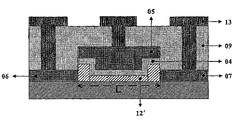
- FIG. 2( b ) shows the implementation of the definition step, wherein a PECVD and LPCVD system are respectively used to stack the gate oxide layer and poly-Si gate region ( 05 ), and a general optical exposure is carried out and RIE etching technique is used, and after defining the gate region ( 05 ), a gate photoresistor ( 03 ) is used as a resistance layer, and the source/drain region ( 07 ) and thin channel region are etched out, and the separation region between the components is completed.
- a PECVD and LPCVD system are respectively used to stack the gate oxide layer and poly-Si gate region ( 05 ), and a general optical exposure is carried out and RIE etching technique is used, and after defining the gate region ( 05 ), a gate photoresistor ( 03 ) is used as a resistance layer, and the source/drain region ( 07 ) and thin channel region are etched out, and the separation region between the components is completed.
- FIG. 2( c ) shows the implementation of the implantation step. Ion implantation is used, completing self-aligned of the heavy doped gate and source/drain region ( 07 ), and ionic activation is carried out using a high temperature stove pipe or laser.
- the PECVD and LPCVD technology can be replaced with high-density plasma apparatus technologies such as ECR-CVD and ICP.
- FIG. 2( d ) shows the implementation of the connection step.
- PECVD is used to deposit the SiO 2 protection layer and open the contact window ( 14 ), and carry out the connection of the aluminum conducting line ( 13 ), thereby completing the production of the novel stacked gate oxide layer TFT.
- the gate photoresistor ( 03 ) region is used for the over etching of the source/drain region ( 07 ) and the channel region, and during this period, there will be a channel region with the same region at the lower side of the gate region ( 05 ) that has been defined.
- the distribution region of the channel will depend on the pre-determined gate region. This characteristic is very important in producing performance components with high space utilization when the region is restricted.
- FIG. 2( e ) refers to the top-view diagram of the completed structure and the important parameters of the component, wherein the parameters of the gate region ( 05 ), source/drain region ( 07 ) and thin channel region are as follows:
- FIG. 2( a ′) shows the second embodiment for the present invention.
- the main difference with the first embodiment is that when the steps in FIG. 2( a ′) are completed, steps 2 ( b ) to 2 ( d ) in the first embodiment are carried out again.
- a LPCVD system is used to deposit a a-Si layer, and a general optical exposure is carried out and RIE etching technique is used, defining the position and size of two independent a-Si islands, and a LPCVD system is used to stack the a-Si film, connecting the two independent a-Si islands, followed by using laser annealing to re-crystallize the a-Si layer to form a poly-Si layer ( 02 ).
- the thickness and operating conditions for the first a-Si layer and the second a-Si thin film layer are as follows:
- Thickness of first layer of a-Si thin film deposit 100-500 nm
- FIG. 3 is the I D -V G switching graph for TFT in the present invention and conventional TFT, and the comparison chart for field-effect mobility, and it can be seen from here that the TFT in the present invention has higher current switching ratio and electron mobility than conventional TFT.
Landscapes
- Thin Film Transistor (AREA)
- Recrystallisation Techniques (AREA)
- Semiconductor Memories (AREA)
Abstract
Description
-
- (1) W″ (Width of gate region (05)): 0.1-200 μm
- (2) W (Width of source/drain region (07) or main channel region): 0.1-200 μm
- (3) L (Length of gate region (05) or overall channels): 0.065-200 μm
- (4) LMC (Length of main channel region): 0.065-200 μm
- (5) Lo.s/Lo.d (Length of channel of gate and source/drain region (07)): 0.065-100 μm
- 01: Thermal oxide layer
- 02,02′,02″;12,12′,12″: poly-Si (layer)
- 03: Photoresistor
- 04: Gate oxide
- 05: Gate region
- 06: Source region
- 07: Drain region
- 08: Implanted poly-Si
- 09: Passivation oxide
- 10: Metal conducting line
- 11: Glass substrate
- 13: Aluminum conducting line
- 14: Contact window
Claims (8)
Applications Claiming Priority (3)
| Application Number | Priority Date | Filing Date | Title |
|---|---|---|---|
| TW95100731A | 2006-01-09 | ||
| TW095100731A TWI316759B (en) | 2006-01-09 | 2006-01-09 | Mothod for fabricatng a straggered source/drain and thin-channel tft |
| TW095100731 | 2006-01-09 |
Publications (2)
| Publication Number | Publication Date |
|---|---|
| US20070161161A1 US20070161161A1 (en) | 2007-07-12 |
| US7678623B2 true US7678623B2 (en) | 2010-03-16 |
Family
ID=38233221
Family Applications (1)
| Application Number | Title | Priority Date | Filing Date |
|---|---|---|---|
| US11/410,168 Expired - Fee Related US7678623B2 (en) | 2006-01-09 | 2006-04-24 | Staggered source/drain and thin-channel TFT structure and fabrication method thereof |
Country Status (3)
| Country | Link |
|---|---|
| US (1) | US7678623B2 (en) |
| JP (1) | JP2007184517A (en) |
| TW (1) | TWI316759B (en) |
Families Citing this family (4)
| Publication number | Priority date | Publication date | Assignee | Title |
|---|---|---|---|---|
| US7851352B2 (en) * | 2007-05-11 | 2010-12-14 | Semiconductor Energy Laboratory Co., Ltd | Manufacturing method of semiconductor device and electronic device |
| JP5371144B2 (en) * | 2007-06-29 | 2013-12-18 | 株式会社半導体エネルギー研究所 | Semiconductor device, method for manufacturing semiconductor device, and electronic device |
| CN101894807B (en) * | 2009-05-22 | 2012-11-21 | 北京京东方光电科技有限公司 | TFT-LCD (Thin Film Transistor-Liquid Crystal Display) array base plate and manufacturing method thereof |
| CN103474472B (en) * | 2013-09-10 | 2016-05-11 | 深圳市华星光电技术有限公司 | A kind of thin film transistor (TFT), array base palte and display floater |
Citations (1)
| Publication number | Priority date | Publication date | Assignee | Title |
|---|---|---|---|---|
| US20080280402A1 (en) * | 2007-05-11 | 2008-11-13 | Semiconductor Energy Laboratory Co., Ltd. | Manufacturing method of semiconductor device and electronic device |
Family Cites Families (2)
| Publication number | Priority date | Publication date | Assignee | Title |
|---|---|---|---|---|
| JP2000216387A (en) * | 1999-01-21 | 2000-08-04 | Sony Corp | Semiconductor device and manufacturing method thereof |
| JP2002033485A (en) * | 2000-05-12 | 2002-01-31 | Matsushita Electric Ind Co Ltd | TFT type liquid crystal display device and method of manufacturing the same |
-
2006
- 2006-01-09 TW TW095100731A patent/TWI316759B/en not_active IP Right Cessation
- 2006-04-24 US US11/410,168 patent/US7678623B2/en not_active Expired - Fee Related
- 2006-05-24 JP JP2006143617A patent/JP2007184517A/en active Pending
Patent Citations (1)
| Publication number | Priority date | Publication date | Assignee | Title |
|---|---|---|---|---|
| US20080280402A1 (en) * | 2007-05-11 | 2008-11-13 | Semiconductor Energy Laboratory Co., Ltd. | Manufacturing method of semiconductor device and electronic device |
Non-Patent Citations (3)
| Title |
|---|
| Kenji Sera, Fujio Oicumura, Hiroyuki Uchida, Shinji Itoh, Setsuo Kaneko, and Kazuaki Hotta, "High-performance TFT'S fabricated by XeCI excimer laser annealing of hydrogenated amorphous-silicon film", IEEE Trans. On Electron Devices, vol. 36, No. 12, pp. 2868-2872, Dec. 1989. (Enclosed). |
| Kwon-Yourig Choi, and Min-Koo Han, A novel gate-overlapped LDD poly-Si thin film transistor IEEE Electron Device Letters, vol. 17, No. 12, pp. 566-568. Dec. 1996. (Enclosed). |
| Po-Sheng Shih, Chun-Yen Chang, Ting-Chang Chang, Tiao-Yuan Huang, Du-Zen Peng, and Ching-Fa Yeh, "A novel lightly doped drain polysilicon thin-film transistor with oxide sidewall spacer formed by one-step selective liquid phase deposition", IEEE Electron Device Letters, vol. 20, No. 8, pp. 421-423, Aug. 1999.(Enclosed). |
Also Published As
| Publication number | Publication date |
|---|---|
| US20070161161A1 (en) | 2007-07-12 |
| TWI316759B (en) | 2009-11-01 |
| JP2007184517A (en) | 2007-07-19 |
| TW200727486A (en) | 2007-07-16 |
Similar Documents
| Publication | Publication Date | Title |
|---|---|---|
| US6916690B2 (en) | Method of fabricating polysilicon film | |
| US7265393B2 (en) | Thin-film transistor with vertical channel region | |
| US7563659B2 (en) | Method of fabricating poly-crystalline silicon thin film and method of fabricating transistor using the same | |
| JP4372993B2 (en) | Manufacturing method of active matrix liquid crystal display device | |
| TWI492315B (en) | A low-temperature polysilicon thin-film transistor manufacturing method | |
| US5834071A (en) | Method for forming a thin film transistor | |
| JP4802364B2 (en) | Semiconductor layer doping method, thin film semiconductor device manufacturing method, and semiconductor layer resistance control method | |
| CN103151388A (en) | Polysilicon TFT (thin film transistor), preparation method thereof and array substrate | |
| JP2002184710A (en) | Semiconductor layer doping method, thin film semiconductor device manufacturing method, and thin film semiconductor device | |
| US9773921B2 (en) | Combo amorphous and LTPS transistors | |
| JP2700277B2 (en) | Method for manufacturing thin film transistor | |
| CN104538455A (en) | Method for manufacturing lightly-doped drain region, thin film transistor and array substrate | |
| US6541323B2 (en) | Method for fabricating polysilicon thin film transistor | |
| CN102054874B (en) | Thin film transistor and manufacturing method thereof | |
| JPH11307777A (en) | Top gate type thin-film transistor and manufacture thereof | |
| US6717178B2 (en) | Semiconductor devices fabricated using sputtered silicon targets | |
| US7678623B2 (en) | Staggered source/drain and thin-channel TFT structure and fabrication method thereof | |
| US20170133512A1 (en) | Polycrystalline silicon thin-film transistor and method for manufacturing the same and display device | |
| CN100413016C (en) | Method for manufacturing polycrystalline silicon thin film | |
| US6982195B2 (en) | Method of forming poly-silicon crystallization | |
| CN101388343A (en) | Thin film transistor and method of manufacturing the same | |
| US20060145158A1 (en) | Poly-crystalline silicon thin film transistor | |
| KR101201316B1 (en) | buffer insulation layer and semiconductor device having the same and method for fabricating of the semiconductor device | |
| JPH11284199A (en) | Semiconductor device and its manufacture | |
| TWI411111B (en) | Thin-film transistor structure and manufacturing method of the same |
Legal Events
| Date | Code | Title | Description |
|---|---|---|---|
| AS | Assignment |
Owner name: NATIONAL CHIAO TUNG UNIVERSITY,TAIWAN Free format text: ASSIGNMENT OF ASSIGNORS INTEREST;ASSIGNORS:CHANG, KOW-MING;LIN, GIN-MIN;SIGNING DATES FROM 20060331 TO 20060406;REEL/FRAME:017622/0241 Owner name: NATIONAL CHIAO TUNG UNIVERSITY, TAIWAN Free format text: ASSIGNMENT OF ASSIGNORS INTEREST;ASSIGNORS:CHANG, KOW-MING;LIN, GIN-MIN;REEL/FRAME:017622/0241;SIGNING DATES FROM 20060331 TO 20060406 |
|
| AS | Assignment |
Owner name: THE REGENTS OF THE UNIVERSITY OF COLORADO, A BODY Free format text: ASSIGNMENT OF ASSIGNORS INTEREST;ASSIGNORS:KRAM, RODGER;MODICA, JESSE R.;GOTTSCHALL, JINGER S.;SIGNING DATES FROM 20060612 TO 20060920;REEL/FRAME:018355/0708 Owner name: THE REGENTS OF THE UNIVERSITY OF COLORADO, A BODY Free format text: ASSIGNMENT OF ASSIGNORS INTEREST;ASSIGNORS:KRAM, RODGER;MODICA, JESSE R.;GOTTSCHALL, JINGER S.;REEL/FRAME:018355/0708;SIGNING DATES FROM 20060612 TO 20060920 |
|
| FPAY | Fee payment |
Year of fee payment: 4 |
|
| FEPP | Fee payment procedure |
Free format text: MAINTENANCE FEE REMINDER MAILED (ORIGINAL EVENT CODE: REM.) |
|
| LAPS | Lapse for failure to pay maintenance fees |
Free format text: PATENT EXPIRED FOR FAILURE TO PAY MAINTENANCE FEES (ORIGINAL EVENT CODE: EXP.) |
|
| STCH | Information on status: patent discontinuation |
Free format text: PATENT EXPIRED DUE TO NONPAYMENT OF MAINTENANCE FEES UNDER 37 CFR 1.362 |
|
| FP | Lapsed due to failure to pay maintenance fee |
Effective date: 20180316 |