US7675497B2 - Driving unit for liquid crystal display device - Google Patents
Driving unit for liquid crystal display device Download PDFInfo
- Publication number
- US7675497B2 US7675497B2 US10/982,779 US98277904A US7675497B2 US 7675497 B2 US7675497 B2 US 7675497B2 US 98277904 A US98277904 A US 98277904A US 7675497 B2 US7675497 B2 US 7675497B2
- Authority
- US
- United States
- Prior art keywords
- ramp signal
- image data
- unit
- significant bit
- bit
- Prior art date
- Legal status (The legal status is an assumption and is not a legal conclusion. Google has not performed a legal analysis and makes no representation as to the accuracy of the status listed.)
- Expired - Fee Related, expires
Links
Images


Classifications
-
- G—PHYSICS
- G09—EDUCATION; CRYPTOGRAPHY; DISPLAY; ADVERTISING; SEALS
- G09G—ARRANGEMENTS OR CIRCUITS FOR CONTROL OF INDICATING DEVICES USING STATIC MEANS TO PRESENT VARIABLE INFORMATION
- G09G3/00—Control arrangements or circuits, of interest only in connection with visual indicators other than cathode-ray tubes
- G09G3/20—Control arrangements or circuits, of interest only in connection with visual indicators other than cathode-ray tubes for presentation of an assembly of a number of characters, e.g. a page, by composing the assembly by combination of individual elements arranged in a matrix no fixed position being assigned to or needed to be assigned to the individual characters or partial characters
- G09G3/34—Control arrangements or circuits, of interest only in connection with visual indicators other than cathode-ray tubes for presentation of an assembly of a number of characters, e.g. a page, by composing the assembly by combination of individual elements arranged in a matrix no fixed position being assigned to or needed to be assigned to the individual characters or partial characters by control of light from an independent source
- G09G3/36—Control arrangements or circuits, of interest only in connection with visual indicators other than cathode-ray tubes for presentation of an assembly of a number of characters, e.g. a page, by composing the assembly by combination of individual elements arranged in a matrix no fixed position being assigned to or needed to be assigned to the individual characters or partial characters by control of light from an independent source using liquid crystals
- G09G3/3611—Control of matrices with row and column drivers
- G09G3/3685—Details of drivers for data electrodes
- G09G3/3688—Details of drivers for data electrodes suitable for active matrices only
-
- G—PHYSICS
- G09—EDUCATION; CRYPTOGRAPHY; DISPLAY; ADVERTISING; SEALS
- G09G—ARRANGEMENTS OR CIRCUITS FOR CONTROL OF INDICATING DEVICES USING STATIC MEANS TO PRESENT VARIABLE INFORMATION
- G09G2320/00—Control of display operating conditions
- G09G2320/02—Improving the quality of display appearance
- G09G2320/0271—Adjustment of the gradation levels within the range of the gradation scale, e.g. by redistribution or clipping
- G09G2320/0276—Adjustment of the gradation levels within the range of the gradation scale, e.g. by redistribution or clipping for the purpose of adaptation to the characteristics of a display device, i.e. gamma correction
-
- G—PHYSICS
- G09—EDUCATION; CRYPTOGRAPHY; DISPLAY; ADVERTISING; SEALS
- G09G—ARRANGEMENTS OR CIRCUITS FOR CONTROL OF INDICATING DEVICES USING STATIC MEANS TO PRESENT VARIABLE INFORMATION
- G09G3/00—Control arrangements or circuits, of interest only in connection with visual indicators other than cathode-ray tubes
- G09G3/20—Control arrangements or circuits, of interest only in connection with visual indicators other than cathode-ray tubes for presentation of an assembly of a number of characters, e.g. a page, by composing the assembly by combination of individual elements arranged in a matrix no fixed position being assigned to or needed to be assigned to the individual characters or partial characters
- G09G3/2007—Display of intermediate tones
- G09G3/2011—Display of intermediate tones by amplitude modulation
Definitions
- the present invention relates to driving a liquid crystal display device, and more particularly, to a driving unit for a LCD device.
- a liquid crystal display (LCD) device in general, includes a liquid crystal display panel formed by attaching a thin film transistor array substrate to a color filter substrate with a uniform gap therebetween. A liquid crystal material fills the gap between the two attached substrates, which face each other.
- the LCD panel also includes a data driving unit for providing image data to the LCD panel and a gate driving unit for providing a scan signal to the LCD panel.
- the thin film transistor array substrate has a plurality of data lines arranged at regular intervals in a first direction and a plurality of gate lines arranged at regular intervals in a second direction, which is orthogonal to the first direction. Pixels are defined by the gate lines and the data lines. Each pixel is provided with a switching device.
- a pixel electrode and a common electrode are provided at the inner surfaces of the thin film transistor array substrate and the color filter substrate that face each others.
- the liquid crystal material between the thin film transistor array substrate and the color filter substrate is driven by a voltage difference between the pixel electrode and the common electrode.
- the brightness of an image displayed on the LCD panel changes in accordance to the voltage of an image data applied to the pixel electrode.
- the pixels are electrically connected to the data lines through the thin film transistors in response to signals on the gate lines. Accordingly, if the scan signal from the gate driving unit are sequentially supplied to the gate lines, the switching device of the pixels connected to the gate lines to which the scan signal are supplied are turned-on, and the data driving unit provides the pixels with image data through the data lines.
- digital image data is used so that the image data can be easily compressed and an image having a high color content and high resolution can be implemented.
- the digital image data can be applied to the LCD device using a ramp signal sampling method or a digital/analog converting method.
- a gamma correction can be more easily done on a pixel in the ramp sampling method by controlling the ramp signals as compared to the digital/analog converting method. Further, a gamma correction in the ramp sampling method does not require an analog circuit.
- ramp signal sampling method analog ramp signals are sampled based upon digital image data, and the sampled signals are supplied to the pixels of the LCD device.
- the ramp signal is a normalized waveform corresponding to the brightness change of an image according to a voltage potential of the image data applied to the LCD device.
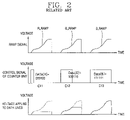
- a related art unit for driving a LCD device using the ramp signal sampling method will be described in detail with reference to FIGS. 1 and 2 .
- FIG. 1 is an exemplary view of a unit for driving a LCD device in which the related art ramp signal sampling method is applied.
- the related art driving unit of the LCD device includes an input register unit 12 for sequentially sampling and storing N-bit digital image data (DATA[R, G and B]) according to control signals (CS 1 to CS 3 ) of a shift register unit 10 ; a counter unit 20 for outputting control signals (C 11 to C 13 ) by individually counting the N-bit digital image data (DATA[R, G and B]) input from the input register unit 12 by a load signal (LOAD) and a clock signal (CLK); and switching units (SW 1 , SW 2 and SW 3 ) for sampling ramp signals (R_RAMP, G_RAMP and B-RAMP) respectively and outputting them to data lines (D 1 , D 2 and D 3 ).
- the operation of the related art unit of driving an LCD device having such construction will be described in detail with reference to a view showing waveforms in FIG. 2 .
- FIG. 2 shows graphs of ramp signals, control signals of the counter unit (shown in FIG. 1 ), and voltages applied to the data lines (shown in FIG. 1 ).
- the input register unit 12 (shown in FIG. 1 ) sequentially samples and store N-bit digital image data (DATA[R, G and B]) according to the control signals (CS 1 to SC 3 ) of the shift register unit 10 .
- the counter unit 20 receives the N-bit digital image data (DAT[R, G and B]) from the input register 10 by the load signal (LOAD), individually counts each bit of the N-bit digital image data (DATA[R, G and B]) by the clock signal CLK and outputs the control signals (C 11 to C 13 ).
- the N-bit digital image data (DATA[R, G and B]) input from the input register 10 by the load signal is stored in a storage latch formed in the counter unit 20 .
- the counter unit 20 is driven by the clock signal (CLK) and counts the digital image data until ‘000000’ becomes ‘000100’, and outputs the control signal (C 11 ), which is at a high potential during the counting of the image data and transitions to a low potential when the counting is completed.
- the 6-bit digital image data (DATA[R, G and B]) is provided as ‘100110’
- the counter unit 20 is driven by the clock signal (CLK) and counts the digital image data until ‘000000’ becomes ‘100110’, and outputs the control signal 12 as a high potential during the counting of the image data and transitions to a low potential when the counting is completed.
- the counter unit 20 is driven by the clock signal (CLK) and counts the digital image data until ‘000000’ becomes ‘111111’, and outputs the control signal 13 as a high potential during the counting of the image data and transitions to a low potential when the counting is completed.
- the switching units (SW 1 , SW 2 and SW 3 ) receive the control signals (C 11 , C 12 and C 13 ) individually from the counter unit 20 and are turned-on by the high potential control signals (C 11 , C 12 and C 13 ) such that sample waveforms of the ramp signal (R_RAMP, G-RAMP and B_RAMP) are supplied to the data lines (D 1 , D 2 and D 3 ).
- the highest potential of the sampled waveforms (R_RAMP, G-RAMP and B_RAMP) according to digital information of the N-bit digital image data (DATA[R, G and B]) is set as a pixel voltage and then supplied to the data lines (D 1 , D 2 and D 3 ).
- the sample waveforms are provided to the pixels of the gate lines turned-on by a scan signal as well as the pixel voltage, which is maintained for one frame.
- a gamma correction on the pixels can be easily performed in comparison to the LCD device using a digital/analog converting method. That is, in the LCD device using the digital/analog converting method, the value of a resistance in an analog device has to be precisely adjusted. However, in the LCD device using the ramp signal sampling method, waveforms of a ramp signal supplied to a pixel can be changed such that the gamma correction can be easily performed.
- the LCD device employing the ramp signal sampling method is not largely affected by characteristic differences of transistors as compared to the LCD device employing the digital/analog converting method, which samples the digital image data as an analog form and applies it to the pixels. That is, the LCD device using the digital/analog converting method requires an analog circuit such as an operational amplifier (OP-AMP) for converting a digital signal to an analog signal. Since the operational amplifier is very sensitive to characteristic differences of the transistors, it has a high offset voltage and consumes much power.
- OP-AMP operational amplifier
- an LCD device using the ramp signal sampling method samples the ramp signal having an analog form according to the digital image data and applies the sampled ramp signal to the pixel
- an LCD device using the ramp signal sampling method does not require the analog circuit such as an operational amplifier and is not largely affected by differences in the characteristics of the transistors.
- the present invention is directed to a driving unit for a LCD device that substantially obviates one or more of the problems due to limitations and disadvantages of the related art.
- An object of the present invention is to provide a driving unit for a LCD device which enables to reduce power consumption by simplifying a design of a counter unit
- Another object is to prevent poor picture quality due to an improper sampling of a ramp signal.
- a driving unit for a LCD device includes: a ramp signal generating unit for dividing a ramp signal into a first ramp signal and a second ramp signal and outputting them; an input register unit for sequentially storing N-bit image data; a counter unit for outputting control signals by receiving bits of image data except for the most significant bit and counting based on the received bits; a ramp signal selecting unit for selecting the first ramp signal or the second ramp signal according to the most significant bit and outputting the selected ramp signal upon receiving the most significant bit from the input register unit; and a switching unit for sampling the first ramp signal or the second ramp signal provided from the ramp signal selecting unit by the control signals of the counter unit and outputting the sampled ramp signal to data lines.
- a driving unit for a LCD device includes: a ramp signal generating unit for dividing a ramp signal into a first ramp signal and a second ramp signal; a data processing unit for selectively reversing and outputting bits exclusive of the most significant bit according to the most significant bit of the image data; an input register unit for sequentially storing N-bit image data provided from the data converting unit; a counter unit for outputting control signals by receiving the N ⁇ 1 bit image data exclusive of the most significant bit from the input register unit and counting based upon the N ⁇ 1 bit image data; a ramp signal selecting unit for selecting the first ramp signal or the second ramp signal according to the most significant bits of the image data from the input register unit and outputting the selected ramp signal; and switching units for sampling the first ramp signal or the second ramp signal provided from the ramp signal selecting unit according to the control signals of the counter unit and outputting the sampled ramp signal to the data lines.
- a method for driving a liquid crystal display device includes: dividing a ramp signal into a first ramp signal and a second ramp signal; sequentially storing N-bit image data into an input register unit; outputting control signals by receiving bits of image data except for the most significant bit (MSB) and counting based upon the received bits; selecting the first ramp signal or the second ramp signal according to the most significant bit received from the input register unit and outputting the selected ramp signal; sampling the first ramp signal or the second ramp signal provided from the ramp signal selecting unit by the control signals of the counter unit; and outputting the sampled ramp signal to data lines.
- MSB most significant bit
- FIG. 1 is a schematic view showing the related art driving unit for a LCD device employing the related art ramp signal sampling method.
- FIG. 2 shows waveforms of the related art ramp signals and control signals of the counter unit and voltages of the data lines shown in FIG. 1 .
- FIG. 3 is an exemplary view showing a driving unit for a LCD device using a ramp signal sampling method in accordance with an embodiment of the present invention.
- FIG. 4 is a schematic showing waveforms of divided ramp signals generated from the ramp signal generating unit of FIG. 3 .
- FIG. 5 is an exemplary view for showing a driving unit for a LCD device using a ramp signal sampling method in accordance with an embodiment of the present invention
- FIG. 6 is a block diagram of the data converting unit in FIG. 5 .
- FIG. 7A is an exemplary view showing one example of the ramp signal selecting unit in FIG. 5 .
- FIG. 7B is an exemplary view showing another example of the ramp signal selecting unit in FIG. 5 .
- FIG. 8 is a view showing waveforms of the divided ramp signals generated from the ramp signal generating unit of FIG. 5 .
- a design of a counter unit for counting according to number of bits in a digital image data becomes complicated when the amount of image data increases as a resolution is raised to display a high-definition image. Also, as each assigned counting section for which a ramp signal is sampled as many as the number of bits increased in a limited entire counting section is reduced, the sampling is completed before the ramp signal reaches a desired level, and due to the distorted sampling of the ramp signal, poor picture quality is generated.
- the driving unit for the LCD device uses a ramp signal that is different from the related art ramp signal.
- FIG. 3 is an exemplary view showing a driving unit for a LCD device using a ramp signal sampling method in accordance with an embodiment of the present invention.
- the unit for driving the LCD device includes a ramp signal generating unit 200 for generating a first ramp signal (R-RAMPH, G_RAMPH or B_RAMPH) and a second ramp signal (R-RAMPL, G_RAMPL or B_RAMPL) from a ramp signal and outputting them; an input register unit 212 for sequentially sampling and storing N-bit image data (DATA[R, G and B]) according to control signals (CS 11 to CS 13 ) of a shift register unit 210 ; a counter unit 220 for outputting control signals (C 111 to C 113 ) by receiving N ⁇ 1 bit image data (DATA[R, G and B]) defining the N-bit image data exclusive of the most significant bit (MSB) from the input register unit 212 according to a load signal (LOAD) and a clock signal (CLK) and individually counting the N
- LOAD
- the input register unit 212 sequentially samples and stores the N-bit image data (DATA[R, G and B]) according to the control signals (CS 11 to CS 13 ) of the shift register unit 210 .
- the counter unit 220 receives N ⁇ 1 bit image data defining the N-bit image data (DATA[R, G and B]) except for the most significant of the image data from the input register unit 210 by the load signal (LOAD), individually counts the N ⁇ 1 bit image data (DATA[R, G and B]) and outputs the control signals (C 111 to C 113 ).
- the control signals are at a high potential during the counting of the N ⁇ 1 bit image data and transition to a low potential when the counting is completed.
- a storage latch provided in the counter unit 220 receives and stores the N ⁇ 1 bit image data (DATA[R, G and B]) from the input register unit 210 according to the load signal (LOAD).
- the counting number is reduced by half in comparison to the related art LCD device, thereby simplifying the design of the counter unit.
- the ramp signal selecting unit 205 receives the most significant bits (R_MSB, G_MSB and B_MSB) of image data (DATA[R, G and B]) from the input register unit 212 , selects the first ramp signal or the second ramp signal and provides the selected ramp signal to the switching units (SW 11 , SW 12 and SW 13 ).
- the switching units (SW 11 , SW 12 and SW 13 ) individually receive the control signals (C 111 , C 112 and C 113 ) from the counter unit 220 and apply waveforms of the ramp signals provided from the ramp signal selecting unit 205 during the high potential section of the control signals (C 111 , C 112 and C 113 ) to the data lines (D 11 , D 12 and D 13 ).
- the highest voltage level of the first ramp signal (R_RAMPH, G_RAMPH or B_RAMPH) or the second ramp signal (R_RAMPL, G_RAMPL or B_RAMPL) that occurred during the high potential section of the control signals is applied to the data lines (D 11 , D 12 and D 13 ) is maintained for one frame after the control signals (C 111 , C 112 and C 113 ) transition from a high potential to a low potential.
- FIG. 4 is a view showing waveforms of divided ramp signals generated from the ramp signal generating unit of FIG. 3 .
- a ramp signal is divided into a first ramp signal and a second ramp signal, and the first ramp signal and the second ramp signal have the same start position for the sampling according to the control signals of the counter unit.
- the ramp signal is generated for one horizontal period, sampled in accordance with the control signals of the counter unit and applied to the data lines.
- the divided first and second ramp signals are generated for one horizontal period.
- the first ramp signal or the second ramp signal selected by the ramp signal selecting unit and input to the switching units is generated for each horizontal period and counted according to the control signals of the counter unit. Since the N ⁇ 1 bit image data alone, the N-bit image data exclusive of the most significant bit, is counted to generate control signals, an allocation for each counting section at which the ramp signal is sampled is increased in an entire counting section. Accordingly, the ramp signal can be sampled after the ramp signal reaches a desired level, improving picture quality.
- FIG. 5 is an exemplary view using a ramp signal sampling method in accordance with an embodiment of the present invention.
- the driving unit for the LCD device includes: a ramp signal generating unit 200 for dividing a ramp signal into a first ramp signal (R_RAMPH, G_RAMPH or B_RAMPH) and a second ramp signal (R_RAMPL, G_RAMPL or B_RAMPL) and outputting them; a data processing unit 303 for selectively reversing and outputting image data (DATA[R, G and B]) of the bits except for the most significant bit according to the most significant bit of the image data (DATA[R, G and B]); an input register unit 312 for receiving and sequentially storing the N-bit image data (DATA[R, G and B]) from the data converting unit 303 according to control signals (CS 21 to CS 23 ) of a shift register unit 310 ; a counter unit 320 for outputting control signals (C 211 to C 213 ) by receiving N ⁇ 1 bit image data (
- the data converting unit 303 selectively reverses and outputs the image data (DATA[R, G and B]) exclusive of the most significant bit according to the most significant bit of the image data (DATA[R, G and B]) which is provided as ‘0’ or ‘1’.
- image data of 6 bits ‘100100’ and ‘011000’ is provided to the data converting unit 303
- the data converting unit 303 reverses bits ‘00100’ except for the most significant bit ‘ 1 ’ from ‘100100’ whose most significant bit is ‘1’ and outputs ‘11011’, and it outputs ‘011000’ whose the most significant bit is ‘0’ as it is.
- Data conversion of the image data exclusive of the most important bits ‘ 0 ’ and ‘ 1 ’ as described above can be performed by inversely reversing image data according to the most important bits ‘ 0 ’ and ‘ 1 ’.
- the input register unit 312 sequentially stores the N-bit image data (DATA[R, G and B]) input from the data converting unit 303 by the control signals (CS 21 to CS 23 ) of the shift register unit 310 .
- the counter unit 320 receives the bits except for the most significant bit, that is, the N ⁇ 1 bit image data (DATA[R, G and B]) from the input register unit 310 by the load signal (LOAD), individually counts the N ⁇ 1 bit image data (DATA[R, G and B]) by the clock signal (CLK) and outputs control signals (C 211 to C 213 ) which is transited from a high potential during the counting the N ⁇ 1 bit image data to a low potential when the counting is completed.
- the counter unit 320 is provided with a storage latch inside itself, receives the N-bit image data (DATA[R, G and B]) from the input register 310 by the load signal (LOAD) and stores it.
- the N ⁇ 1 bit image data (DATA[R, G and B]) defining the N-bit image data exclusive of the most significant bit is counted in the counter unit 320 , so that the counting number is reduced by half in comparison to the related art N-bit image data (DATA[R, G and B]).
- the ramp signal selecting unit 305 receives the most significant bits (R_MSB, G_MSB and B_MSB) of the image data (DATA[R, G and B]) from the input register unit 312 , selects the first ramp signal (R_RAMPH, G_RAMPH or B_RAMPH) or the second ramp signal (R_RAMPL, G_RAMPL or B_RAMPL) and provides the selected ramp signal with the switching units (SW 21 , SW 22 and SW 23 ).
- the switching units (SW 21 , SW 22 and SW 23 ) individually receive the control signals (C 211 , C 212 and C 213 ) from the counter unit 320 , sample waveforms of the first ramp signal (R_RAMPH, G_RAMPH and B_RAMPH) or the second ramp signal (R_RAMPL, G_RAMPL and B_RAMPL) selectively provided from the ramp signal selecting unit 305 during a high potential section of the control signals (C 211 , C 212 and C 213 ), and applies the sampled waveform to the data lines (D 21 , D 22 and D 23 ).
- FIG. 6 is a block diagram of a data processing unit.
- the data processing unit includes an image data dividing unit 400 for dividing image data into first image data and second image data according to the most significant bit of N-bit image data and outputting it; a data converting unit 410 for reversing bits except for the most significant bit and outputting them upon receiving the second image data input from the image data dividing unit 400 ; and a multiplexer 420 for selectively outputting the first image data or the second image data out of the first image data directly input from the image data dividing unit 400 and the second image data reversed and then input from the data converting unit 410 according to a selection signal SS 11 of the image data dividing unit 400 .
- the image data dividing unit 400 divides the N-bit image data into the first image data and the second image data according to the most significant bit (MSB) of the N-bit image data, and provides the first image data to the multiplexer 420 and the second image data to the data converting unit 410 .
- the data converting unit 410 receiving the second image data reverses the bits exclusive of the most significant bit of the second image data and applies them to the multiplexer 420 .
- image data provided to the image data dividing unit 400 is designated as 6-bit image data.
- image data dividing unit 400 divides the image data into the first image data and the second data according to the most significant bit of the image data and outputs the divided the first and second image data.
- the data converting unit 410 reverses the second image data and outputs it to the multiplexer 420 as stated above. For instance, when the second image data is designated as ‘010110’, the bits except for the most significant bit is reversed and thus ‘001001’ is output from the data converting unit 410 .
- the multiplexer 420 receives the first image data from the image data dividing unit 400 and the second image data, in which the bits exclusive of the most significant bit (MSB) are reversed, from the data converting unit 410 .
- the multiplexer 420 selects the first image data or the second image data according to the selection signal SS 11 of the image data dividing unit 400 and outputs the selected image data.
- the counter unit receives the first image data or the second image selectively output from the data processing unit, counts it and applies the control signals to the switching units.
- the switching units sample the first lamp signal or the second ramp signal according to the control signals input from the counter unit.
- the ramp signal selecting unit receives the most significant bit (MSB) of the N-bit image data from the input register unit, selects the first ramp signal or the second ramp signal according to the most significant bit (MSB) and applies the selected ramp signal to the switching units.
- MSB most significant bit
- the ramp signal selecting unit will be described in detain with reference to the accompanying drawings.
- FIG. 7A is an exemplary view showing one example of the ramp signal selecting unit in the FIG. 5 .
- FIG. 7B is an exemplary view showing another example of the ramp signal selecting unit in the FIG. 5 .
- the first ramp signal (RAMPH) and the second ramp signal (RAMPL) are supplied through supply lines, respectively.
- the supply lines are electrically connected to the switching devices (T 11 and T 12 ) using a transistor, such as a MOSFET (metal oxide semiconductor field effect transistor).
- the switching devices (T 11 and T 12 ) are turned-on or turned-off according to the most significant bit (MSB) provided from the input register of the unit for driving the LCD device, and the first ramp signal (RAMPH) or the second ramp signal (RAMPL) is provided to the switching unit according to the turned-on switching devices (T 11 and T 12 ).
- MSB most significant bit
- the switching unit samples the first ramp signal (RAMPH) or the second ramp signal (RAMPL) from the ramp signal selecting unit according to the most significant bit (MSB) of the image data.
- the switching devices (T 11 and T 12 ) receives the most significant bit (MSB) of the image data through a gate electrode and the first ramp signal (RAMPH) or the second ramp signal (RAMPL) through a source electrode.
- the switching devices (T 11 and T 12 ) comprise different types of transistors. Accordingly, one of the switching devices is turned-on according to the most significant bit (MSB) of the image data input from the input register unit, receives the first ramp signal (RAMPH) or the second ramp signal (RAMPL) through the source electrode and outputs the supplied ramp signal to the switching units through the drain electrode.
- a P-type switching device T 11
- receives the second ramp signal RAMPL
- a N-type switching device T 12
- the P-type switching device (T 11 ) and the N-type switching device (T 12 ) operate apposite to each other in relation to the low potential voltage or the high potential voltage of the most significant bit (MSB) of the image data, whereby one signal out of the first ramp signal (RAMPH) and the second ramp signal (RAMPL) is passed.
- the P-type and the N-type switching (T 11 and T 12 ) can be in exchanged positions.
- FIG. 7B shows another example of a ramp signal selecting unit using N-type switching devices (T 21 and T 22 ) having the same polarity. As shown in FIG. 7B , different types of switching devices are used in FIG. 7A , while two identical N-type switching devices are used in FIG. 7B . One of the switching devices is electrically connected to an inverter 500 .
- the ramp signal selecting unit comprises the same N-type switching devices (T 21 and T 22 ) and has the same operational effect as the ramp signal selecting unit of FIG. 7A .
- both of the ramp signal selecting units have different constructions, provision of the inverter 500 and connection with the different type transistor result in the same operation. For example, if the most significant bit (MSB) ‘ 0 ’ of image data is provided from the input register, that is, a low potential is provided, a high potential reversed from the inverter 500 is input to the switching device (T 21 ) connected to the inverter 500 to turn-on the switching device (T 21 ), and a low potential is applied to the other switching device (T 22 ), turning-off the switching device (T 22 ). Namely, the switching device (T 21 ) to which the inverter 500 is connected is turned-on, and thus the second ramp signal (RAMPL) is sampled by the switching unit.
- MSB most significant bit
- a low potential voltage reversed and then output from the inverter 500 is applied to the switching device (T 21 ) connected to the inverter 500 to turn off the switching device (T 21 ), and a high potential voltage is applied to the other switching device (T 22 ), turning-on the switching device (T 22 ) That is, the second ramp signal (RAMPL) alone passes through the N-type switching device (T 21 ) using the inverter 500 and is sampled by the switching unit.
- FIG. 8 is a view showing waveforms of divided ramp signals generated from the ramp signal generating unit of FIG. 5 .
- two adjacent gray scale points in the divided ramp signals, (A) and (B), and (C) and (D) show the same gray scale but have differences in their sampling time. That is, there are certain time differences from when sampling of the divided ramp signals starts at the point (A) or (C) to when the sampling of the same starts at the point (B) or (D). Accordingly, there is difference of gray scale between the two points.
- the divided ramp signals of FIG. 8 are waveforms that address the problems of simply divided ramp signals, as shown in FIG. 4 .
- a ramp signal is divided into a first ramp signal and a second ramp signal and output from a ramp signal generating unit (not shown).
- the second ramp signal defines a reversed second ramp signal of simply divided ramp signals and has the same sampling position as the first ramp signal according to the control signal of the counter unit. That is, the second ramp signal is reversed whereby the first ramp signal and the second ramp signal show the identical gray scale at one point (( 1 ) and ( 2 )). Accordingly, the problem of two points showing different gray scales actually is solved.
- the control signal of the counter unit is generated according to waveforms of the original ramp signal before the second ramp signal is reversed.
- the control signal of the counter unit does not coincide with a start point of sampling the second ramp signal, the second ramp signal is not sampled properly, and accordingly a desired image cannot be displayed properly.
- the image data should be converted according to the first ramp signal or the second ramp signal as shown in the data converting unit of FIG. 6 and counted in the counter unit. Namely, when the first image data output without processing is counted in the counter unit, the first ramp signal whose sampling start point is not changed is sampled according to the first image data.
- the second ramp signal is sampled according to the second image data.
- the second image data By counting the reversed second image data and corresponding the counted second image data to the start point of sampling the reversed second ramp signal, it is possible to sample the ramp signal having a desired level.
- the ramp signal is divided and the divided image data corresponding to the divided ramp signal is counted only, and thus the number of the bits of the image data to be counted is reduced less than the half, thereby simplifying a design of the counter unit and reducing power consumption.
Landscapes
- Engineering & Computer Science (AREA)
- Chemical & Material Sciences (AREA)
- Crystallography & Structural Chemistry (AREA)
- Physics & Mathematics (AREA)
- Computer Hardware Design (AREA)
- General Physics & Mathematics (AREA)
- Theoretical Computer Science (AREA)
- Control Of Indicators Other Than Cathode Ray Tubes (AREA)
- Liquid Crystal (AREA)
- Liquid Crystal Display Device Control (AREA)
Abstract
Description
Claims (5)
Applications Claiming Priority (3)
| Application Number | Priority Date | Filing Date | Title |
|---|---|---|---|
| KR1020030079132A KR100618582B1 (en) | 2003-11-10 | 2003-11-10 | Drive part of LCD |
| KR10-2003-0079132 | 2003-11-10 | ||
| KRP2003-79132 | 2003-11-10 |
Publications (2)
| Publication Number | Publication Date |
|---|---|
| US20050099381A1 US20050099381A1 (en) | 2005-05-12 |
| US7675497B2 true US7675497B2 (en) | 2010-03-09 |
Family
ID=34545818
Family Applications (1)
| Application Number | Title | Priority Date | Filing Date |
|---|---|---|---|
| US10/982,779 Expired - Fee Related US7675497B2 (en) | 2003-11-10 | 2004-11-08 | Driving unit for liquid crystal display device |
Country Status (4)
| Country | Link |
|---|---|
| US (1) | US7675497B2 (en) |
| JP (1) | JP4176702B2 (en) |
| KR (1) | KR100618582B1 (en) |
| CN (1) | CN100382135C (en) |
Cited By (5)
| Publication number | Priority date | Publication date | Assignee | Title |
|---|---|---|---|---|
| US20090251299A1 (en) * | 2005-09-27 | 2009-10-08 | Hidetaka Mizumaki | Liquid crystal display device, instrument panel, automotive vehicle, and liquid crystal display method |
| US20100225518A1 (en) * | 2006-11-07 | 2010-09-09 | Yusuke Tokunaga | Digital/analog converter circuit |
| US20120081340A1 (en) * | 2010-10-04 | 2012-04-05 | Nex-I Solution. Co., Ltd | Driver and display device having the same |
| US20180211605A1 (en) * | 2017-01-25 | 2018-07-26 | Samsung Display Co., Ltd. | Data driver and display device having the same |
| US10896652B2 (en) * | 2017-12-18 | 2021-01-19 | Sharp Kabushiki Kaisha | Display control device and liquid crystal display device including display control device |
Families Citing this family (11)
| Publication number | Priority date | Publication date | Assignee | Title |
|---|---|---|---|---|
| KR101157950B1 (en) | 2005-09-29 | 2012-06-25 | 엘지디스플레이 주식회사 | Apparatus and method for driving image display device using the same |
| KR101147121B1 (en) * | 2005-11-21 | 2012-05-25 | 엘지디스플레이 주식회사 | Apparatus and method for transmission data, apparatus and method for driving image display device using the same |
| TWI348134B (en) * | 2006-05-18 | 2011-09-01 | Chunghwa Picture Tubes Ltd | A data driver and a data driving method of a flat panel display device |
| CN101079241B (en) * | 2006-05-23 | 2012-08-08 | 中华映管股份有限公司 | Data driver of flat panel display device and driving method thereof |
| US8896590B2 (en) * | 2006-09-05 | 2014-11-25 | Sharp Kabushiki Kaisha | Display controller, display device, and control method for controlling display system and display device |
| KR100840074B1 (en) | 2007-02-02 | 2008-06-20 | 삼성에스디아이 주식회사 | Data driver and flat panel display using same |
| JP5439782B2 (en) * | 2008-09-29 | 2014-03-12 | セイコーエプソン株式会社 | Pixel circuit driving method, light emitting device, and electronic apparatus |
| US9747834B2 (en) * | 2012-05-11 | 2017-08-29 | Ignis Innovation Inc. | Pixel circuits including feedback capacitors and reset capacitors, and display systems therefore |
| JP6095955B2 (en) * | 2012-11-16 | 2017-03-15 | ルネサスエレクトロニクス株式会社 | Measuring method, measuring apparatus and measuring program |
| CN114677954B (en) * | 2022-03-04 | 2024-05-31 | 富满微电子集团股份有限公司 | Signal selection circuit and LED driving chip |
| CN115775535B (en) * | 2022-11-30 | 2023-10-03 | 南京国兆光电科技有限公司 | Display driving circuit |
Citations (10)
| Publication number | Priority date | Publication date | Assignee | Title |
|---|---|---|---|---|
| JPH06314080A (en) | 1993-04-14 | 1994-11-08 | Internatl Business Mach Corp <Ibm> | Liquid-crystal display device |
| US5828357A (en) * | 1996-03-27 | 1998-10-27 | Sharp Kabushiki Kaisha | Display panel driving method and display apparatus |
| US6049320A (en) * | 1996-07-27 | 2000-04-11 | Lg Electronics Inc. | Data driver for use in liquid crystal display |
| US6137462A (en) * | 1996-05-02 | 2000-10-24 | Lg Electronics Inc. | Liquid crystal display driving circuit |
| EP1047039A1 (en) * | 1998-10-16 | 2000-10-25 | Seiko Epson Corporation | Driver circuit of electro-optical device, driving method, d/a converter, signal driver, electro-optical panel, projection display, and electronic device |
| US6384806B1 (en) * | 1998-03-24 | 2002-05-07 | Seiko Epson Corporation | Digital driver circuit for electro-optical device and electro-optical device having the digital driver circuit |
| JP2002533788A (en) | 1998-12-28 | 2002-10-08 | コーニンクレッカ フィリップス エレクトロニクス エヌ ヴィ | Compensation of sampling error in photoelectric display device |
| US6724379B2 (en) * | 2001-06-08 | 2004-04-20 | Eastman Kodak Company | Multichannel driver circuit for a spatial light modulator and method of calibration |
| US6778163B2 (en) * | 2000-12-28 | 2004-08-17 | Seiko Epson Corporation | Liquid crystal display device, driving circuit, driving method, and electronic apparatus |
| JP2005529369A (en) | 2002-06-10 | 2005-09-29 | コーニンクレッカ フィリップス エレクトロニクス エヌ ヴィ | Load adaptive column driver |
Family Cites Families (3)
| Publication number | Priority date | Publication date | Assignee | Title |
|---|---|---|---|---|
| US5170155A (en) * | 1990-10-19 | 1992-12-08 | Thomson S.A. | System for applying brightness signals to a display device and comparator therefore |
| US5673063A (en) * | 1995-03-06 | 1997-09-30 | Thomson Consumer Electronics, S.A. | Data line driver for applying brightness signals to a display |
| US6429858B1 (en) * | 2000-03-29 | 2002-08-06 | Koninklijke Philips Electronics N.V. | Apparatus having a DAC-controlled ramp generator for applying voltages to individual pixels in a color electro-optic display device |
-
2003
- 2003-11-10 KR KR1020030079132A patent/KR100618582B1/en not_active Expired - Fee Related
-
2004
- 2004-11-08 US US10/982,779 patent/US7675497B2/en not_active Expired - Fee Related
- 2004-11-10 JP JP2004325766A patent/JP4176702B2/en not_active Expired - Lifetime
- 2004-11-10 CN CNB2004100886466A patent/CN100382135C/en not_active Expired - Fee Related
Patent Citations (11)
| Publication number | Priority date | Publication date | Assignee | Title |
|---|---|---|---|---|
| JPH06314080A (en) | 1993-04-14 | 1994-11-08 | Internatl Business Mach Corp <Ibm> | Liquid-crystal display device |
| US5477234A (en) * | 1993-04-14 | 1995-12-19 | International Business Machines Corporation | Liquid crystal display apparatus |
| US5828357A (en) * | 1996-03-27 | 1998-10-27 | Sharp Kabushiki Kaisha | Display panel driving method and display apparatus |
| US6137462A (en) * | 1996-05-02 | 2000-10-24 | Lg Electronics Inc. | Liquid crystal display driving circuit |
| US6049320A (en) * | 1996-07-27 | 2000-04-11 | Lg Electronics Inc. | Data driver for use in liquid crystal display |
| US6384806B1 (en) * | 1998-03-24 | 2002-05-07 | Seiko Epson Corporation | Digital driver circuit for electro-optical device and electro-optical device having the digital driver circuit |
| EP1047039A1 (en) * | 1998-10-16 | 2000-10-25 | Seiko Epson Corporation | Driver circuit of electro-optical device, driving method, d/a converter, signal driver, electro-optical panel, projection display, and electronic device |
| JP2002533788A (en) | 1998-12-28 | 2002-10-08 | コーニンクレッカ フィリップス エレクトロニクス エヌ ヴィ | Compensation of sampling error in photoelectric display device |
| US6778163B2 (en) * | 2000-12-28 | 2004-08-17 | Seiko Epson Corporation | Liquid crystal display device, driving circuit, driving method, and electronic apparatus |
| US6724379B2 (en) * | 2001-06-08 | 2004-04-20 | Eastman Kodak Company | Multichannel driver circuit for a spatial light modulator and method of calibration |
| JP2005529369A (en) | 2002-06-10 | 2005-09-29 | コーニンクレッカ フィリップス エレクトロニクス エヌ ヴィ | Load adaptive column driver |
Cited By (8)
| Publication number | Priority date | Publication date | Assignee | Title |
|---|---|---|---|---|
| US20090251299A1 (en) * | 2005-09-27 | 2009-10-08 | Hidetaka Mizumaki | Liquid crystal display device, instrument panel, automotive vehicle, and liquid crystal display method |
| US8339345B2 (en) * | 2005-09-27 | 2012-12-25 | Sharp Kabushiki Kaisha | Liquid crystal display device, instrument panel, automotive vehicle, and liquid crystal display method |
| US20100225518A1 (en) * | 2006-11-07 | 2010-09-09 | Yusuke Tokunaga | Digital/analog converter circuit |
| US7936295B2 (en) * | 2006-11-07 | 2011-05-03 | Panasonic Corporation | Digital/analog converter circuit |
| US20120081340A1 (en) * | 2010-10-04 | 2012-04-05 | Nex-I Solution. Co., Ltd | Driver and display device having the same |
| US20180211605A1 (en) * | 2017-01-25 | 2018-07-26 | Samsung Display Co., Ltd. | Data driver and display device having the same |
| US10593269B2 (en) * | 2017-01-25 | 2020-03-17 | Samsung Display Co., Ltd. | Data driver and display device having the same |
| US10896652B2 (en) * | 2017-12-18 | 2021-01-19 | Sharp Kabushiki Kaisha | Display control device and liquid crystal display device including display control device |
Also Published As
| Publication number | Publication date |
|---|---|
| KR100618582B1 (en) | 2006-08-31 |
| US20050099381A1 (en) | 2005-05-12 |
| CN100382135C (en) | 2008-04-16 |
| JP4176702B2 (en) | 2008-11-05 |
| JP2005148733A (en) | 2005-06-09 |
| CN1624752A (en) | 2005-06-08 |
| KR20050045168A (en) | 2005-05-17 |
Similar Documents
| Publication | Publication Date | Title |
|---|---|---|
| US7675497B2 (en) | Driving unit for liquid crystal display device | |
| US7102610B2 (en) | Display system with frame buffer and power saving sequence | |
| US8305313B2 (en) | Liquid crystal display apparatus, and driving circuit and driving method thereof | |
| US6424331B1 (en) | Driving circuit for electro-optical device, driving method therefor, DA converter, signal line driving circuit, electro-optical panel, projection type display device, and electronic equipment | |
| US20010024199A1 (en) | Controller circuit for liquid crystal matrix display devices | |
| US20080136964A1 (en) | Electro-optical device, scan line driving circuit, and electronic apparatus | |
| US6963325B2 (en) | Display driving apparatus with compensating current and liquid crystal display apparatus using the same | |
| JPH10145706A (en) | Clamp / gamma correction circuit, image display device and electronic device using the same | |
| KR100495934B1 (en) | Display driving apparatus and driving control method | |
| JP5382178B2 (en) | Driving circuit for liquid crystal display device | |
| JP2006343563A (en) | Liquid crystal display device | |
| JPH01107237A (en) | Liquid crystal display device | |
| JP2001201732A (en) | Liquid crystal display device | |
| US7692644B2 (en) | Display apparatus | |
| TWI427583B (en) | Sequential colour matrix liquid crystal display | |
| JP2854620B2 (en) | Driving method of display device | |
| US20110001735A1 (en) | Electro-optical device, method for driving electro-optical device and electronic apparatus | |
| US20030210239A1 (en) | Drive circuit for electro-optical device, method of driving electro-optical device,electro-optical apparatus, and electronic appliance | |
| JPH07199156A (en) | Liquid crystal display device | |
| JPH07199157A (en) | Liquid crystal display device | |
| JPH11175038A (en) | Driving method for display device and driving circuit therefor | |
| JP2000172234A (en) | Electro-optical device driving circuit, electro-optical device, and electro-optical device driving method | |
| JPH0725829Y2 (en) | Liquid crystal drive | |
| JP2004070367A (en) | Liquid crystal display | |
| JPH07191635A (en) | Active matrix liquid crystal display panel driving method |
Legal Events
| Date | Code | Title | Description |
|---|---|---|---|
| AS | Assignment |
Owner name: LG.PHILIPS LCD CO., LTD., KOREA, REPUBLIC OF Free format text: ASSIGNMENT OF ASSIGNORS INTEREST;ASSIGNOR:PARK, JOON-KYU;REEL/FRAME:015966/0208 Effective date: 20041103 Owner name: LG.PHILIPS LCD CO., LTD.,KOREA, REPUBLIC OF Free format text: ASSIGNMENT OF ASSIGNORS INTEREST;ASSIGNOR:PARK, JOON-KYU;REEL/FRAME:015966/0208 Effective date: 20041103 |
|
| AS | Assignment |
Owner name: LG DISPLAY CO., LTD., KOREA, REPUBLIC OF Free format text: CHANGE OF NAME;ASSIGNOR:LG.PHILIPS LCD CO., LTD.;REEL/FRAME:021754/0045 Effective date: 20080304 Owner name: LG DISPLAY CO., LTD.,KOREA, REPUBLIC OF Free format text: CHANGE OF NAME;ASSIGNOR:LG.PHILIPS LCD CO., LTD.;REEL/FRAME:021754/0045 Effective date: 20080304 |
|
| FEPP | Fee payment procedure |
Free format text: PAYOR NUMBER ASSIGNED (ORIGINAL EVENT CODE: ASPN); ENTITY STATUS OF PATENT OWNER: LARGE ENTITY |
|
| STCF | Information on status: patent grant |
Free format text: PATENTED CASE |
|
| FPAY | Fee payment |
Year of fee payment: 4 |
|
| FPAY | Fee payment |
Year of fee payment: 8 |
|
| FEPP | Fee payment procedure |
Free format text: MAINTENANCE FEE REMINDER MAILED (ORIGINAL EVENT CODE: REM.); ENTITY STATUS OF PATENT OWNER: LARGE ENTITY |
|
| LAPS | Lapse for failure to pay maintenance fees |
Free format text: PATENT EXPIRED FOR FAILURE TO PAY MAINTENANCE FEES (ORIGINAL EVENT CODE: EXP.); ENTITY STATUS OF PATENT OWNER: LARGE ENTITY |
|
| STCH | Information on status: patent discontinuation |
Free format text: PATENT EXPIRED DUE TO NONPAYMENT OF MAINTENANCE FEES UNDER 37 CFR 1.362 |
|
| FP | Lapsed due to failure to pay maintenance fee |
Effective date: 20220309 |